Copyright Agrawal, 2007 ELEC6270 Fall 07, Lecture 13 1 ELEC 5270/6270 Fall 2007 Low-Power Design of...
23
Copyright Agrawal, 2007 Copyright Agrawal, 2007 ELEC6270 Fall 07, Lecture 13 ELEC6270 Fall 07, Lecture 13 1 ELEC 5270/6270 Fall 2007 ELEC 5270/6270 Fall 2007 Low-Power Design of Electronic Low-Power Design of Electronic Circuits Circuits Pseudo-nMOS, Dynamic CMOS Pseudo-nMOS, Dynamic CMOS and Domino CMOS Logic and Domino CMOS Logic Vishwani D. Agrawal Vishwani D. Agrawal James J. Danaher Professor James J. Danaher Professor Dept. of Electrical and Computer Engineering Dept. of Electrical and Computer Engineering Auburn University, Auburn, AL 36849 Auburn University, Auburn, AL 36849 [email protected] http://www.eng.auburn.edu/~vagrawal/COURSE/E6270_Fall07/ course.html
-
date post
21-Dec-2015 -
Category
Documents
-
view
213 -
download
0
Transcript of Copyright Agrawal, 2007 ELEC6270 Fall 07, Lecture 13 1 ELEC 5270/6270 Fall 2007 Low-Power Design of...

Copyright Agrawal, 2007Copyright Agrawal, 2007 ELEC6270 Fall 07, Lecture 13ELEC6270 Fall 07, Lecture 13 11
ELEC 5270/6270 Fall 2007ELEC 5270/6270 Fall 2007Low-Power Design of Electronic CircuitsLow-Power Design of Electronic Circuits
Pseudo-nMOS, Dynamic CMOSPseudo-nMOS, Dynamic CMOSand Domino CMOS Logicand Domino CMOS Logic
Vishwani D. AgrawalVishwani D. AgrawalJames J. Danaher ProfessorJames J. Danaher Professor
Dept. of Electrical and Computer EngineeringDept. of Electrical and Computer EngineeringAuburn University, Auburn, AL 36849Auburn University, Auburn, AL 36849
[email protected]://www.eng.auburn.edu/~vagrawal/COURSE/E6270_Fall07/course.html

Copyright Agrawal, 2007Copyright Agrawal, 2007 ELEC6270 Fall 07, Lecture 13ELEC6270 Fall 07, Lecture 13 22
Why Not Static CMOS?Why Not Static CMOS?
Advantages: Static (robust) operation, low Advantages: Static (robust) operation, low power, scalable with technology.power, scalable with technology.
Disadvantages:Disadvantages: Large size: An N input gate requires 2N transistors.Large size: An N input gate requires 2N transistors. Large capacitance: Each fanout must drive two Large capacitance: Each fanout must drive two
devices.devices.
Alternatives: Pass-transistor logic (PTL), Alternatives: Pass-transistor logic (PTL), pseudo-nMOS, dynamic CMOS, domino CMOS. pseudo-nMOS, dynamic CMOS, domino CMOS.
Copyright Agrawal, 2007Copyright Agrawal, 2007 ELEC6270 Fall 07, Lecture 13ELEC6270 Fall 07, Lecture 13 33
A Pseudo-nMOS GateA Pseudo-nMOS Gate
PUN
PDN
VDD
CMOS Gate
PDN
VDD
Pseudo-nMOS Gate
Output
Inp
uts
Inp
uts
Output

Copyright Agrawal, 2007Copyright Agrawal, 2007 ELEC6270 Fall 07, Lecture 13ELEC6270 Fall 07, Lecture 13 44
Pseudo-nMOS NORPseudo-nMOS NOR
VDD
Input 1
Output
Input 2 Input 3

Copyright Agrawal, 2007Copyright Agrawal, 2007 ELEC6270 Fall 07, Lecture 13ELEC6270 Fall 07, Lecture 13 55
Pseudo-nMOS NANDPseudo-nMOS NANDVDD
Input 1
Output
Input 2
Copyright Agrawal, 2007Copyright Agrawal, 2007 ELEC6270 Fall 07, Lecture 13ELEC6270 Fall 07, Lecture 13 66
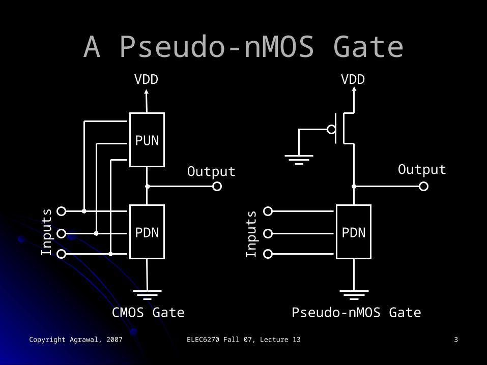
Pseudo-nMOS InverterPseudo-nMOS Inverter
VDD
Input
Output

Copyright Agrawal, 2007Copyright Agrawal, 2007 ELEC6270 Fall 07, Lecture 13ELEC6270 Fall 07, Lecture 13 77
Inverter CharacteristicsInverter Characteristics
W/Lp = 4
W/Lp = 2
W/Lp = 0.25
W/Lp
= 0.5W/Lp
= 1
0.0 0.5 1.0 1.5 2.0 2.5
Input voltage, V
Ou
tpu
t vo
ltag
e, V
3.0
2.5
2.0
1.5
1.0
0.5
0.0
Nominal device: W 0.5μ── = ──── = 2 Ln 0.25μ

Copyright Agrawal, 2007Copyright Agrawal, 2007 ELEC6270 Fall 07, Lecture 13ELEC6270 Fall 07, Lecture 13 88
Performance of InverterPerformance of InverterSize, W/LSize, W/Lpp Logic 0 voltageLogic 0 voltage Logic 0 static Logic 0 static
powerpowerDelayDelay
0 → 10 → 1
44 0.693 V0.693 V 564 564 μμWW 14 ps14 ps
22 0.273 V0.273 V 298 298 μμWW 56 ps56 ps
11 0.133 V0.133 V 160 160 μμWW 123 ps123 ps
0.50.5 0.064 V0.064 V 80 80 μμWW 268 ps268 ps
0.250.25 0.031 V0.031 V 41 41 μμWW 569 ps569 ps
J. M. Rabaey, A. Chandrakasan and B. Nokolić, Digital IntegratedCircuits, Upper Saddle River, New Jersey: Pearson Education, 2003, page 262.

Copyright Agrawal, 2007Copyright Agrawal, 2007 ELEC6270 Fall 07, Lecture 13ELEC6270 Fall 07, Lecture 13 99
Negative Aspects of Pseudo-nMOSNegative Aspects of Pseudo-nMOS
Output 0 state is ratioed logic.Output 0 state is ratioed logic.Faster gates mean higher static power.Faster gates mean higher static power.Low static power means slow gates.Low static power means slow gates.

Copyright Agrawal, 2007Copyright Agrawal, 2007 ELEC6270 Fall 07, Lecture 13ELEC6270 Fall 07, Lecture 13 1010
A Dynamic CMOS GateA Dynamic CMOS Gate
PDN
VDD
Inp
uts
Output
CK
CL
Prechargetransistor
Evaluatetransistor
Copyright Agrawal, 2007Copyright Agrawal, 2007 ELEC6270 Fall 07, Lecture 13ELEC6270 Fall 07, Lecture 13 1111
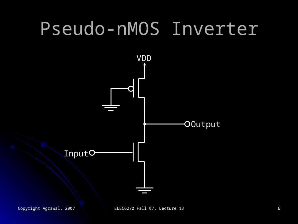
Two-Phase Operation in a Vector Two-Phase Operation in a Vector PeriodPeriod
PhasePhase CKCK InputsInputs OutputOutput
PrechargePrecharge lowlow don’t caredon’t care highhigh
EvaluationEvaluation highhigh Valid inputsValid inputs Valid outputsValid outputs

Copyright Agrawal, 2007Copyright Agrawal, 2007 ELEC6270 Fall 07, Lecture 13ELEC6270 Fall 07, Lecture 13 1212
4-Input NAND Dynamic CMOS Gate4-Input NAND Dynamic CMOS Gate
Output= CK’ + (ABCD)’∙ CK
CL
CK
A
B
C
D
CK
VDD
tL→H ≈ 0

Copyright Agrawal, 2007Copyright Agrawal, 2007 ELEC6270 Fall 07, Lecture 13ELEC6270 Fall 07, Lecture 13 1313
Characteristics of Dynamic CMOSCharacteristics of Dynamic CMOS
Nonratioed logic – sizing of pMOS transistor is not important Nonratioed logic – sizing of pMOS transistor is not important for output levels.for output levels.
Smaller number of transistors, N+2 vs. 2N.Smaller number of transistors, N+2 vs. 2N. Larger precharge transistor reduces output fall time, but Larger precharge transistor reduces output fall time, but
increases precharge power. Faster switching due to smaller increases precharge power. Faster switching due to smaller capacitance.capacitance.
Static power – negligible.Static power – negligible. Short-circuit power – none.Short-circuit power – none. Dynamic powerDynamic power
no glitches – following precharge, signals can either make transitions no glitches – following precharge, signals can either make transitions only in one direction, 1→0, or no transition, 1→1.only in one direction, 1→0, or no transition, 1→1.
only logic transitions – all nodes at logic 0 are charged to VDD during only logic transitions – all nodes at logic 0 are charged to VDD during precharge phase.precharge phase.
Copyright Agrawal, 2007Copyright Agrawal, 2007 ELEC6270 Fall 07, Lecture 13ELEC6270 Fall 07, Lecture 13 1414
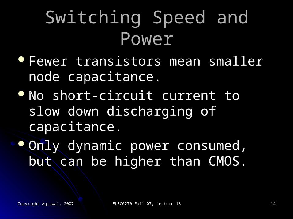
Switching Speed and PowerSwitching Speed and Power
Fewer transistors mean smaller node Fewer transistors mean smaller node capacitance.capacitance.
No short-circuit current to slow down No short-circuit current to slow down discharging of capacitance.discharging of capacitance.
Only dynamic power consumed, but can Only dynamic power consumed, but can be higher than CMOS.be higher than CMOS.
Copyright Agrawal, 2007Copyright Agrawal, 2007 ELEC6270 Fall 07, Lecture 13ELEC6270 Fall 07, Lecture 13 1515
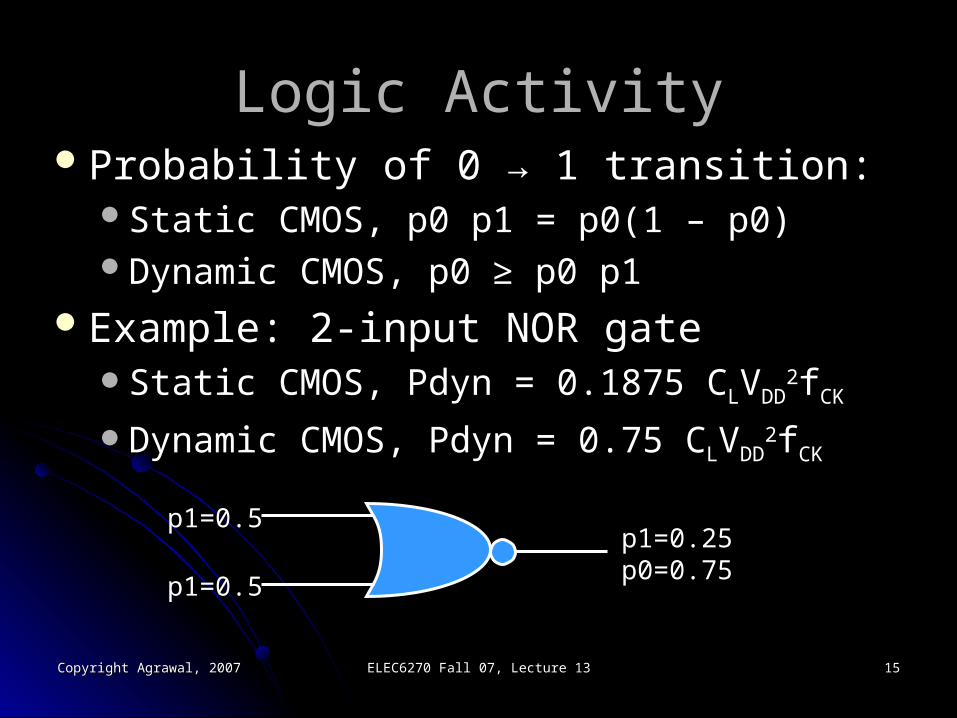
Logic ActivityLogic ActivityProbability of 0 → 1 transition:Probability of 0 → 1 transition:
Static CMOS, p0 p1 = p0(1 – p0)Static CMOS, p0 p1 = p0(1 – p0)Dynamic CMOS, p0 Dynamic CMOS, p0 ≥ p0 p1≥ p0 p1
Example: 2-input NOR gateExample: 2-input NOR gateStatic CMOS, Pdyn = 0.1875 CStatic CMOS, Pdyn = 0.1875 CLLVVDDDD
22ffCKCK
Dynamic CMOS, Pdyn = 0.75 CDynamic CMOS, Pdyn = 0.75 CLLVVDDDD22ffCKCK
p1=0.5
p1=0.5
p1=0.25 p0=0.75

Copyright Agrawal, 2007Copyright Agrawal, 2007 ELEC6270 Fall 07, Lecture 13ELEC6270 Fall 07, Lecture 13 1616
Charge LeakageCharge Leakage
OutputA’
CL
CK
A=0
CK
VDD
CK
A’
TimeP
rech
arg
e
Eva
luat
e
IdealActual
J. M. Rabaey, A. Chandrakasan and B. Nokolić, Digital IntegratedCircuits, Upper Saddle River, New Jersey: Pearson Education, 2003.

Copyright Agrawal, 2007Copyright Agrawal, 2007 ELEC6270 Fall 07, Lecture 13ELEC6270 Fall 07, Lecture 13 1717
Bleeder TransistorBleeder Transistor
Output
CL
CK
A
B
C
D
CK
VDD
Output
CL
CK
A
B
C
D
CK
VDD

Copyright Agrawal, 2007Copyright Agrawal, 2007 ELEC6270 Fall 07, Lecture 13ELEC6270 Fall 07, Lecture 13 1818
A Problems With Dynamic CMOSA Problems With Dynamic CMOS
CK
A=0→1
CK
VDDCK
A
B
C
B
J. M. Rabaey, A. Chandrakasan and B. Nokolić, Digital IntegratedCircuits, Upper Saddle River, New Jersey: Pearson Education, 2003.
CK
CK
VDD
C
prech. evaluate

Copyright Agrawal, 2007Copyright Agrawal, 2007 ELEC6270 Fall 07, Lecture 13ELEC6270 Fall 07, Lecture 13 1919
RemedyRemedy
Set all inputs to gates to 0 during Set all inputs to gates to 0 during precharge.precharge.
Since precharge raises all outputs to 1, Since precharge raises all outputs to 1, inserting inverters between gates will do inserting inverters between gates will do the trick.the trick.
Copyright Agrawal, 2007Copyright Agrawal, 2007 ELEC6270 Fall 07, Lecture 13ELEC6270 Fall 07, Lecture 13 2020
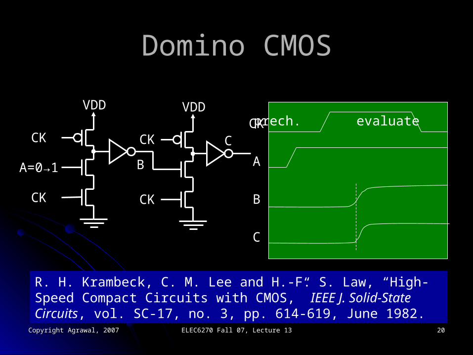
Domino CMOSDomino CMOS
CK
A=0→1
CK
VDD
CK
A
B
C
B
R. H. Krambeck, C. M. Lee and H.-F. S. Law, “High-Speed Compact Circuits with CMOS,” IEEE J. Solid-State Circuits, vol. SC-17, no. 3, pp. 614-619, June 1982.
CK
CK
VDD
C
prech. evaluate

Copyright Agrawal, 2007Copyright Agrawal, 2007 ELEC6270 Fall 07, Lecture 13ELEC6270 Fall 07, Lecture 13 2121
Bleeder in Domino CMOSBleeder in Domino CMOS
Output
CL
CK
A
B
C
D
CK
VDD
Copyright Agrawal, 2007Copyright Agrawal, 2007 ELEC6270 Fall 07, Lecture 13ELEC6270 Fall 07, Lecture 13 2222
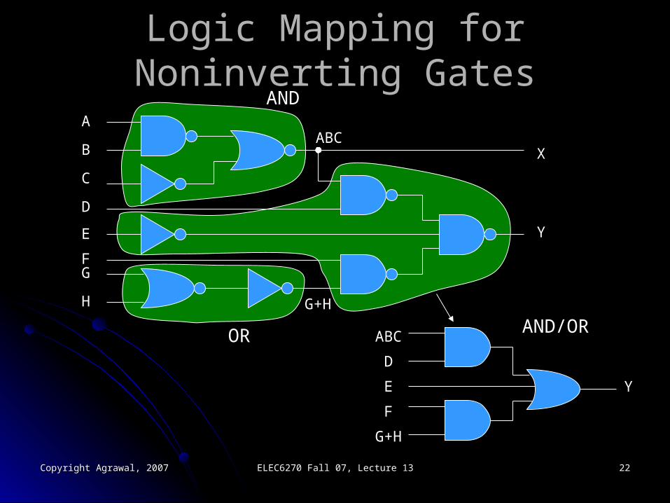
Logic Mapping for Noninverting GatesLogic Mapping for Noninverting Gates
A
B
C
D
E
FG
H
ABC
G+H
AND
OR AND/OR
X
Y
Y
ABC
D
E
F
G+H

Copyright Agrawal, 2007Copyright Agrawal, 2007 ELEC6270 Fall 07, Lecture 13ELEC6270 Fall 07, Lecture 13 2323
Selecting a Logic StyleSelecting a Logic Style Static CMOS: most reliable and predictable, Static CMOS: most reliable and predictable,
reasonable in power and speed, voltage scaling reasonable in power and speed, voltage scaling and device sizing are well understood.and device sizing are well understood.
Pass-transistor logic: beneficial for multiplexer Pass-transistor logic: beneficial for multiplexer and XOR dominated circuits like adders, etc.and XOR dominated circuits like adders, etc.
For large fanin gates, static CMOS is inefficient; For large fanin gates, static CMOS is inefficient; a choice can be made between pseudo-nMOS, a choice can be made between pseudo-nMOS, dynamic CMOS and domino CMOS.dynamic CMOS and domino CMOS.