Fall 2006, Nov. 30 ELEC 5270-001/6270-001 Lecture 12 1 ELEC 5270-001/6270-001(Fall 2006) Low-Power...
25
Fall 2006, Nov. 30 Fall 2006, Nov. 30 ELEC 5270-001/6270-001 Lect ELEC 5270-001/6270-001 Lect ure 12 ure 12 1 ELEC 5270-001/6270-001(Fall ELEC 5270-001/6270-001(Fall 2006) 2006) Low-Power Design of Electronic Circuits Low-Power Design of Electronic Circuits Test Power Test Power Vishwani D. Agrawal Vishwani D. Agrawal James J. Danaher Professor James J. Danaher Professor Department of Electrical and Computer Department of Electrical and Computer Engineering Engineering Auburn University, Auburn, AL 36849 Auburn University, Auburn, AL 36849 http://www.eng.auburn.edu/~vagrawal http://www.eng.auburn.edu/~vagrawal [email protected] [email protected]
-
date post
20-Dec-2015 -
Category
Documents
-
view
216 -
download
3
Transcript of Fall 2006, Nov. 30 ELEC 5270-001/6270-001 Lecture 12 1 ELEC 5270-001/6270-001(Fall 2006) Low-Power...
Fall 2006, Nov. 30Fall 2006, Nov. 30 ELEC 5270-001/6270-001 Lecture 12ELEC 5270-001/6270-001 Lecture 12 11
ELEC 5270-001/6270-001(Fall ELEC 5270-001/6270-001(Fall 2006)2006)
Low-Power Design of Electronic CircuitsLow-Power Design of Electronic Circuits
Test PowerTest Power
Vishwani D. AgrawalVishwani D. AgrawalJames J. Danaher ProfessorJames J. Danaher Professor
Department of Electrical and Computer Department of Electrical and Computer EngineeringEngineering
Auburn University, Auburn, AL 36849Auburn University, Auburn, AL 36849http://www.eng.auburn.edu/~vagrawalhttp://www.eng.auburn.edu/~vagrawal
[email protected]@eng.auburn.edu
Fall 2006, Nov. 30Fall 2006, Nov. 30 ELEC 5270-001/6270-001 Lecture 12ELEC 5270-001/6270-001 Lecture 12 22
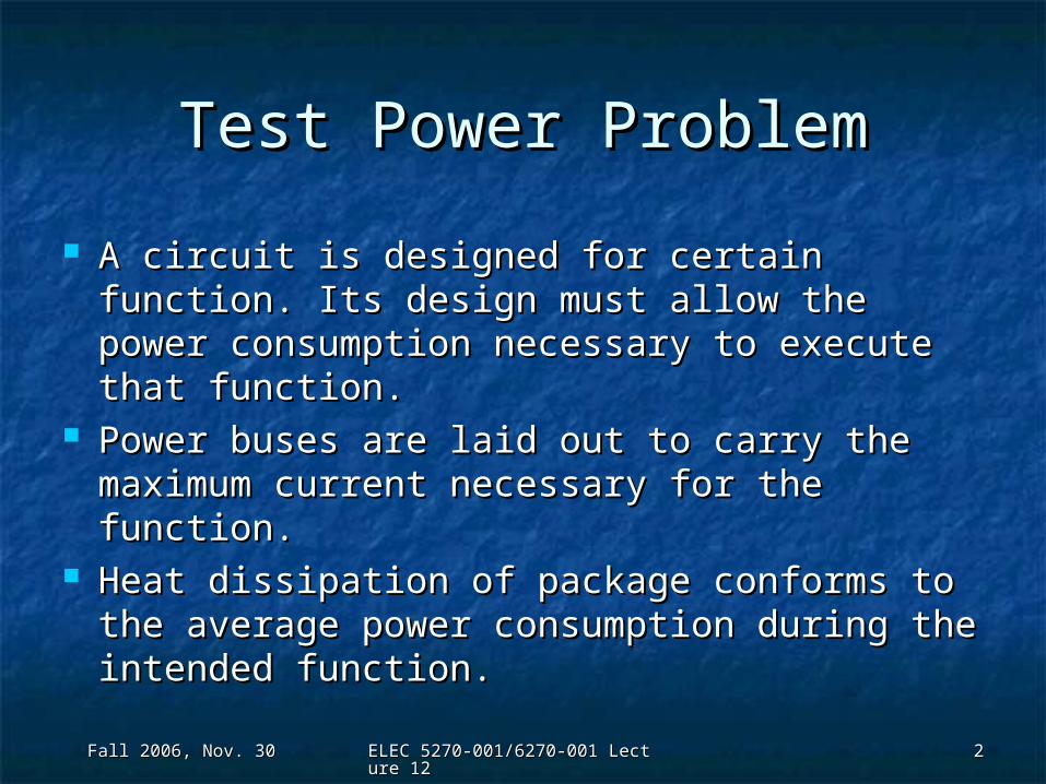
Test Power ProblemTest Power Problem
A circuit is designed for certain function. Its A circuit is designed for certain function. Its design must allow the power consumption design must allow the power consumption necessary to execute that function.necessary to execute that function.
Power buses are laid out to carry the Power buses are laid out to carry the maximum current necessary for the function.maximum current necessary for the function.
Heat dissipation of package conforms to the Heat dissipation of package conforms to the average power consumption during the average power consumption during the intended function.intended function.
Fall 2006, Nov. 30Fall 2006, Nov. 30 ELEC 5270-001/6270-001 Lecture 12ELEC 5270-001/6270-001 Lecture 12 33
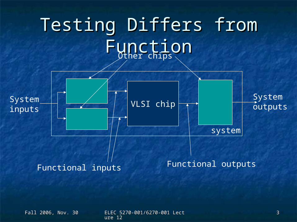
Testing Differs from Testing Differs from FunctionFunction
VLSI chip
system
Systeminputs
Systemoutputs
Functional inputs Functional outputs
Other chips
Fall 2006, Nov. 30Fall 2006, Nov. 30 ELEC 5270-001/6270-001 Lecture 12ELEC 5270-001/6270-001 Lecture 12 44
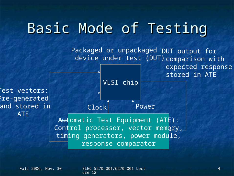
Basic Mode of TestingBasic Mode of Testing
VLSI chipTest vectors:
Pre-generated and stored in
ATE
DUT output for comparison with expected response stored in ATE
Automatic Test Equipment (ATE):Control processor, vector memory,timing generators, power module,
response comparator
PowerClock
Packaged or unpackaged device under test (DUT)
Fall 2006, Nov. 30Fall 2006, Nov. 30 ELEC 5270-001/6270-001 Lecture 12ELEC 5270-001/6270-001 Lecture 12 55
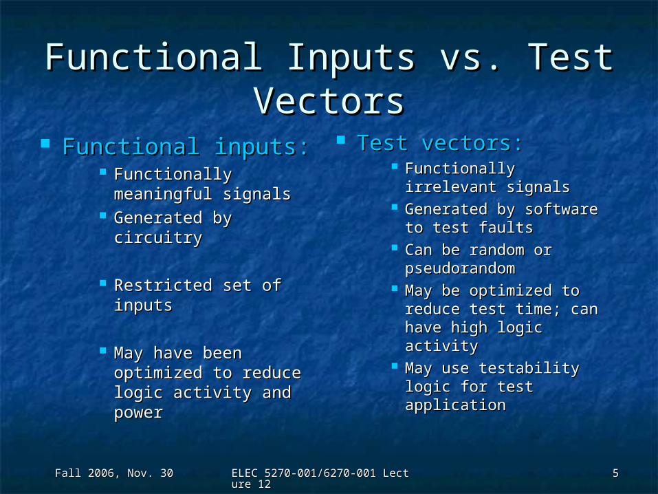
Functional Inputs vs. Test Functional Inputs vs. Test VectorsVectors
Functional inputs:Functional inputs: Functionally Functionally
meaningful signalsmeaningful signals Generated by circuitryGenerated by circuitry
Restricted set of Restricted set of inputsinputs
May have been May have been optimized to reduce optimized to reduce logic activity and logic activity and powerpower
Test vectors:Test vectors: Functionally irrelevant Functionally irrelevant
signalssignals Generated by software Generated by software
to test faultsto test faults Can be random or Can be random or
pseudorandompseudorandom May be optimized to May be optimized to
reduce test time; can reduce test time; can have high logic activityhave high logic activity
May use testability May use testability logic for test logic for test applicationapplication
Fall 2006, Nov. 30Fall 2006, Nov. 30 ELEC 5270-001/6270-001 Lecture 12ELEC 5270-001/6270-001 Lecture 12 66
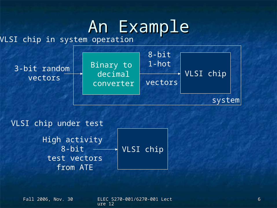
An ExampleAn Example
VLSI chipBinary to decimal
converter
3-bit random vectors
8-bit1-hot
vectors
VLSI chip
system
VLSI chip in system operation
VLSI chip under test
High activity8-bit
test vectors from ATE
Fall 2006, Nov. 30Fall 2006, Nov. 30 ELEC 5270-001/6270-001 Lecture 12ELEC 5270-001/6270-001 Lecture 12 77
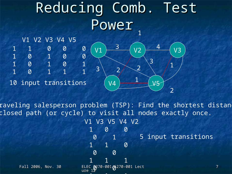
Reducing Comb. Test Power Reducing Comb. Test Power
1 1 0 0 01 0 1 0 01 0 1 0 11 0 1 1 1
V1 V2 V3
V4 V5
3 4
1
3 223
2
1
1
V1 V2 V3 V4 V5
10 input transitions
Traveling salesperson problem (TSP): Find the shortest distance closed path (or cycle) to visit all nodes exactly once.
V1 V3 V5 V4 V21 0 0 0 11 1 0 0 01 1 1 0 01 1 1 1 0
5 input transitions
Fall 2006, Nov. 30Fall 2006, Nov. 30 ELEC 5270-001/6270-001 Lecture 12ELEC 5270-001/6270-001 Lecture 12 88
Traveling Salesperson Traveling Salesperson ProblemProblem
A. V. Aho, J. E. Hopcroft anf J. D. A. V. Aho, J. E. Hopcroft anf J. D. Ullman, Ullman, Data Structures and Data Structures and AlgorithmsAlgorithms, Reading, Massachusetts: , Reading, Massachusetts: Addison-Wesley, 1983.Addison-Wesley, 1983.
E. Horowitz and S. Sahni, E. Horowitz and S. Sahni, Fundamentals of Computer Fundamentals of Computer AlgorithmsAlgorithms, Computer Science Press, , Computer Science Press, 1984.1984.
Fall 2006, Nov. 30Fall 2006, Nov. 30 ELEC 5270-001/6270-001 Lecture 12ELEC 5270-001/6270-001 Lecture 12 99
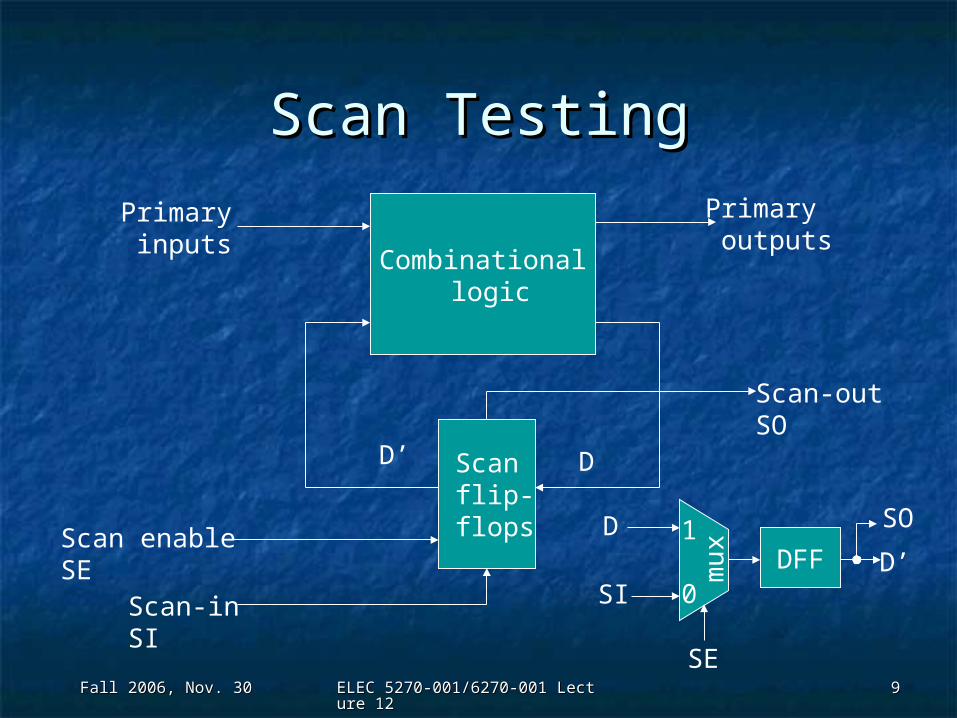
Scan TestingScan Testing
Combinational logic
Scan flip- flops
Primary inputs
Primary outputs
Scan-inSI
Scan-outSO
Scan enableSE DFF
mu
x
SE
SI
D
D
D’
D’
SO1
0
Fall 2006, Nov. 30Fall 2006, Nov. 30 ELEC 5270-001/6270-001 Lecture 12ELEC 5270-001/6270-001 Lecture 12 1010
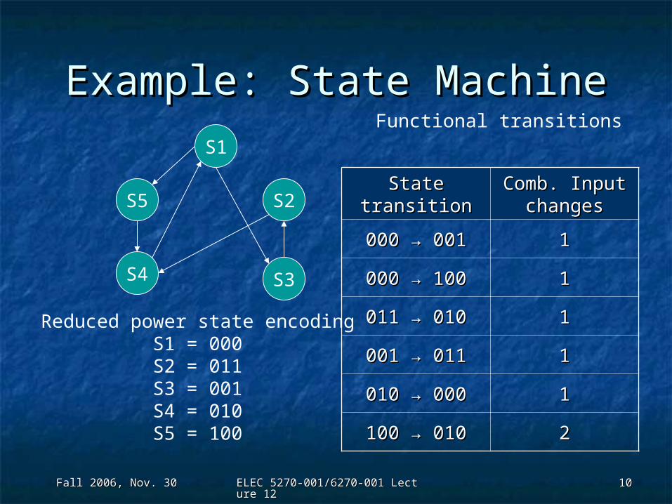
Example: State MachineExample: State Machine
S5
S1
S4
S2
S3
Reduced power state encodingS1 = 000S2 = 011S3 = 001S4 = 010S5 = 100
State State transitiontransition
Comb. Input Comb. Input changeschanges
000 → 001000 → 001 11
000 → 100000 → 100 11
011 → 010011 → 010 11
001 → 011001 → 011 11
010 → 000010 → 000 11
100 → 010100 → 010 22
Functional transitions
Fall 2006, Nov. 30Fall 2006, Nov. 30 ELEC 5270-001/6270-001 Lecture 12ELEC 5270-001/6270-001 Lecture 12 1111
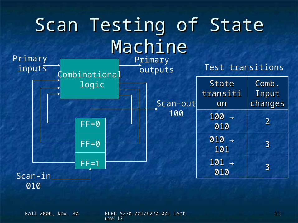
Scan Testing of State Scan Testing of State MachineMachine
Combinational logic
FF=0
FF=0
FF=1
Primary inputs
Primary outputs
Scan-in010
Scan-out100
State State transitiontransition
Comb. Comb. Input Input
changeschanges
100 → 010100 → 010 22
010 → 101010 → 101 33
101 → 010101 → 010 33
Test transitions
Fall 2006, Nov. 30Fall 2006, Nov. 30 ELEC 5270-001/6270-001 Lecture 12ELEC 5270-001/6270-001 Lecture 12 1212
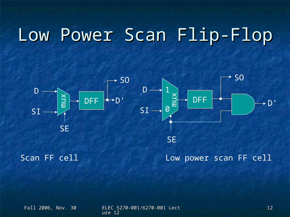
Low Power Scan Flip-FlopLow Power Scan Flip-Flop
DFF
mu
x
SE
SI
DDFFm
ux
SE
SI
DSO
D’ D’
SO
Scan FF cell Low power scan FF cell
1
0
Fall 2006, Nov. 30Fall 2006, Nov. 30 ELEC 5270-001/6270-001 Lecture 12ELEC 5270-001/6270-001 Lecture 12 1313
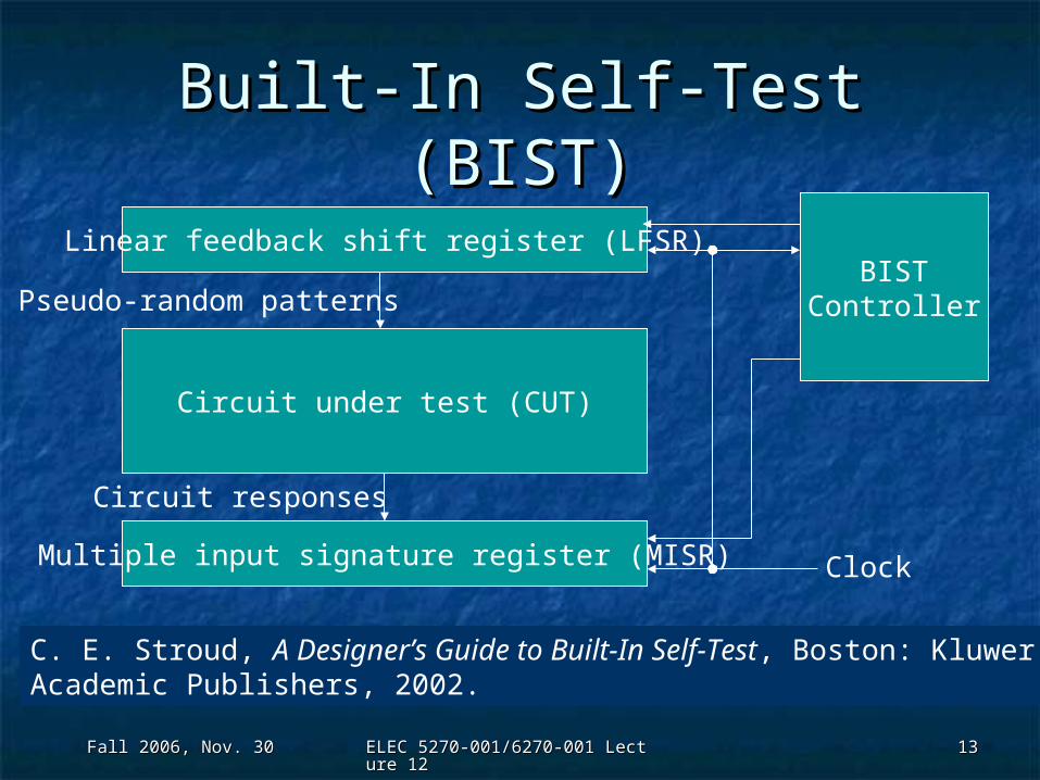
Built-In Self-Test (BIST)Built-In Self-Test (BIST)
Linear feedback shift register (LFSR)
Multiple input signature register (MISR)
Circuit under test (CUT)
Pseudo-random patterns
Circuit responses
BISTController
Clock
C. E. Stroud, A Designer’s Guide to Built-In Self-Test, Boston: KluwerAcademic Publishers, 2002.
Fall 2006, Nov. 30Fall 2006, Nov. 30 ELEC 5270-001/6270-001 Lecture 12ELEC 5270-001/6270-001 Lecture 12 1414
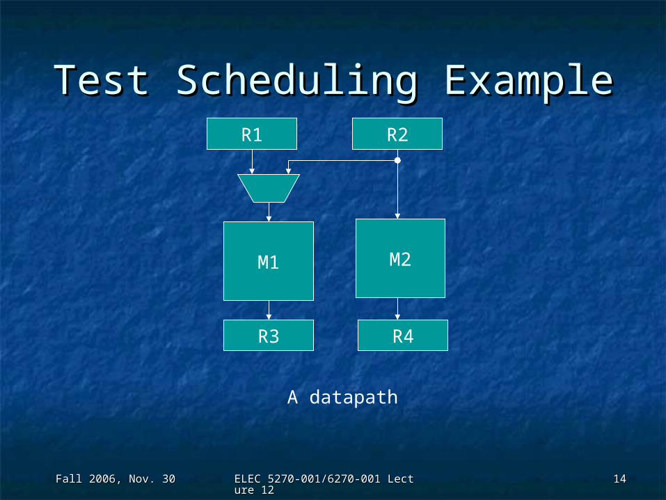
Test Scheduling ExampleTest Scheduling ExampleR1 R2
M1 M2
R3 R4
A datapath
Fall 2006, Nov. 30Fall 2006, Nov. 30 ELEC 5270-001/6270-001 Lecture 12ELEC 5270-001/6270-001 Lecture 12 1515
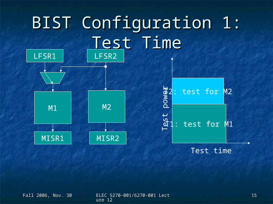
BIST Configuration 1: Test BIST Configuration 1: Test TimeTime
LFSR1 LFSR2
M1 M2
MISR1 MISR2
Test time
Te
st p
ow
er
T1: test for M1
T2: test for M2
Fall 2006, Nov. 30Fall 2006, Nov. 30 ELEC 5270-001/6270-001 Lecture 12ELEC 5270-001/6270-001 Lecture 12 1616
BIST Configuration 2: Test BIST Configuration 2: Test PowerPower
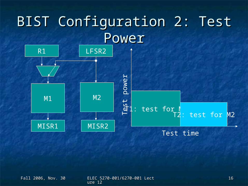
R1 LFSR2
M1 M2
MISR1 MISR2Test time
Te
st p
ow
er
T1: test for M1T2: test for M2
Fall 2006, Nov. 30Fall 2006, Nov. 30 ELEC 5270-001/6270-001 Lecture 12ELEC 5270-001/6270-001 Lecture 12 1717
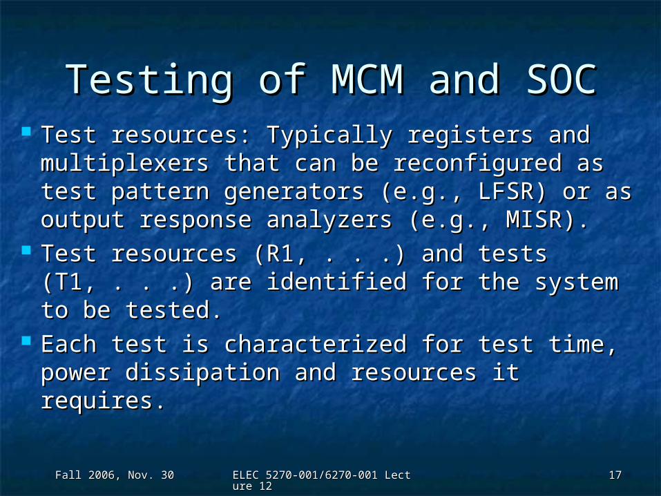
Testing of MCM and SOCTesting of MCM and SOC Test resources: Typically registers and Test resources: Typically registers and
multiplexers that can be reconfigured as multiplexers that can be reconfigured as test pattern generators (e.g., LFSR) or as test pattern generators (e.g., LFSR) or as output response analyzers (e.g., MISR).output response analyzers (e.g., MISR).
Test resources (R1, . . .) and tests (T1, . . .) Test resources (R1, . . .) and tests (T1, . . .) are identified for the system to be tested.are identified for the system to be tested.
Each test is characterized for test time, Each test is characterized for test time, power dissipation and resources it power dissipation and resources it requires.requires.
Fall 2006, Nov. 30Fall 2006, Nov. 30 ELEC 5270-001/6270-001 Lecture 12ELEC 5270-001/6270-001 Lecture 12 1818
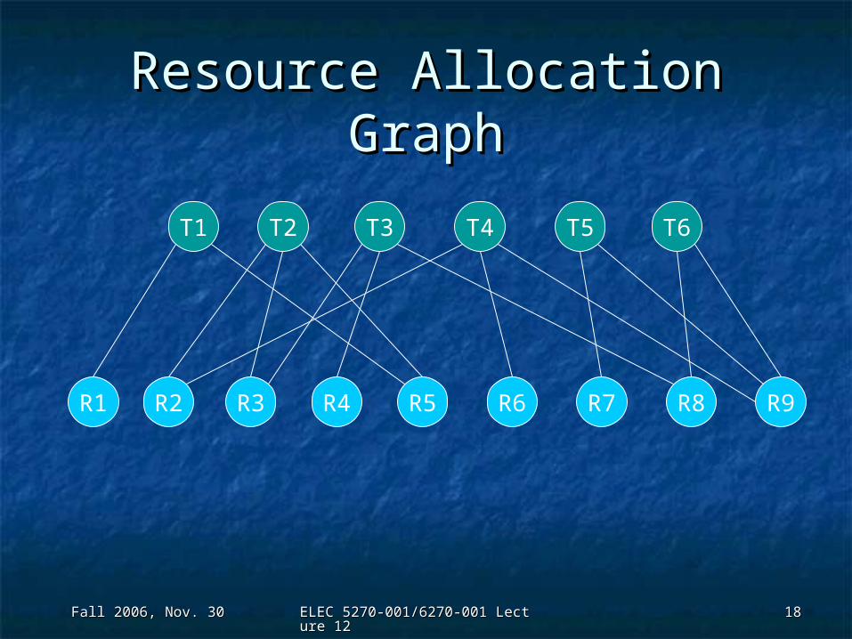
Resource Allocation GraphResource Allocation Graph
T1 T2 T3 T4 T5 T6
R2R1 R3 R4 R5 R6 R7 R8 R9
Fall 2006, Nov. 30Fall 2006, Nov. 30 ELEC 5270-001/6270-001 Lecture 12ELEC 5270-001/6270-001 Lecture 12 1919
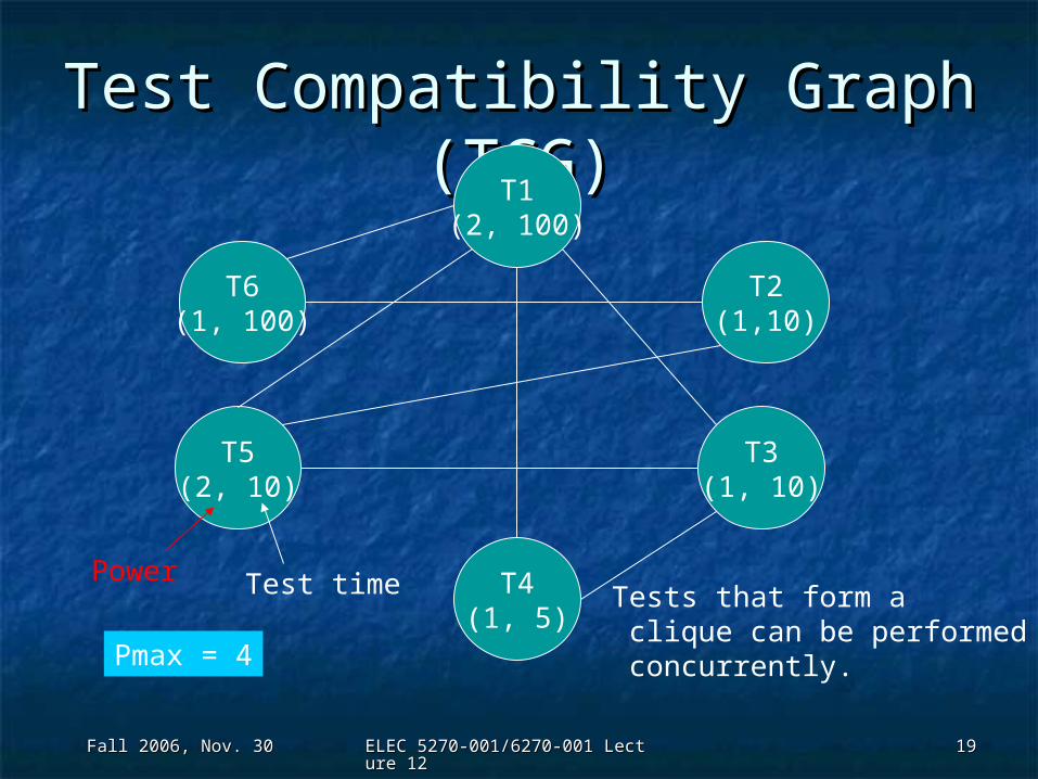
Test Compatibility Graph Test Compatibility Graph (TCG)(TCG)T1
(2, 100)
T2(1,10)
T3(1, 10)
T4(1, 5)
T5(2, 10)
T6(1, 100)
Tests that form a clique can be performed concurrently.
Power Test time
Pmax = 4
Fall 2006, Nov. 30Fall 2006, Nov. 30 ELEC 5270-001/6270-001 Lecture 12ELEC 5270-001/6270-001 Lecture 12 2020
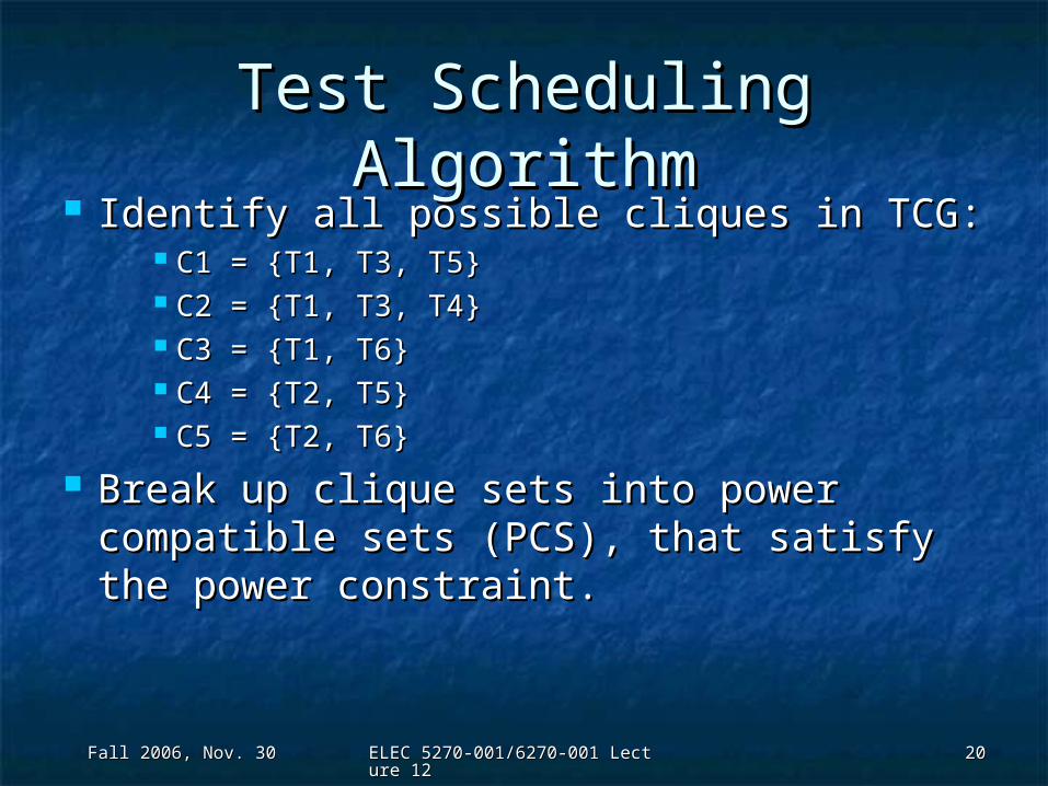
Test Scheduling AlgorithmTest Scheduling Algorithm Identify all possible cliques in TCG:Identify all possible cliques in TCG:
C1 = {T1, T3, T5}C1 = {T1, T3, T5} C2 = {T1, T3, T4}C2 = {T1, T3, T4} C3 = {T1, T6}C3 = {T1, T6} C4 = {T2, T5}C4 = {T2, T5} C5 = {T2, T6}C5 = {T2, T6}
Break up clique sets into power Break up clique sets into power compatible sets (PCS), that satisfy the compatible sets (PCS), that satisfy the power constraint.power constraint.
Fall 2006, Nov. 30Fall 2006, Nov. 30 ELEC 5270-001/6270-001 Lecture 12ELEC 5270-001/6270-001 Lecture 12 2121
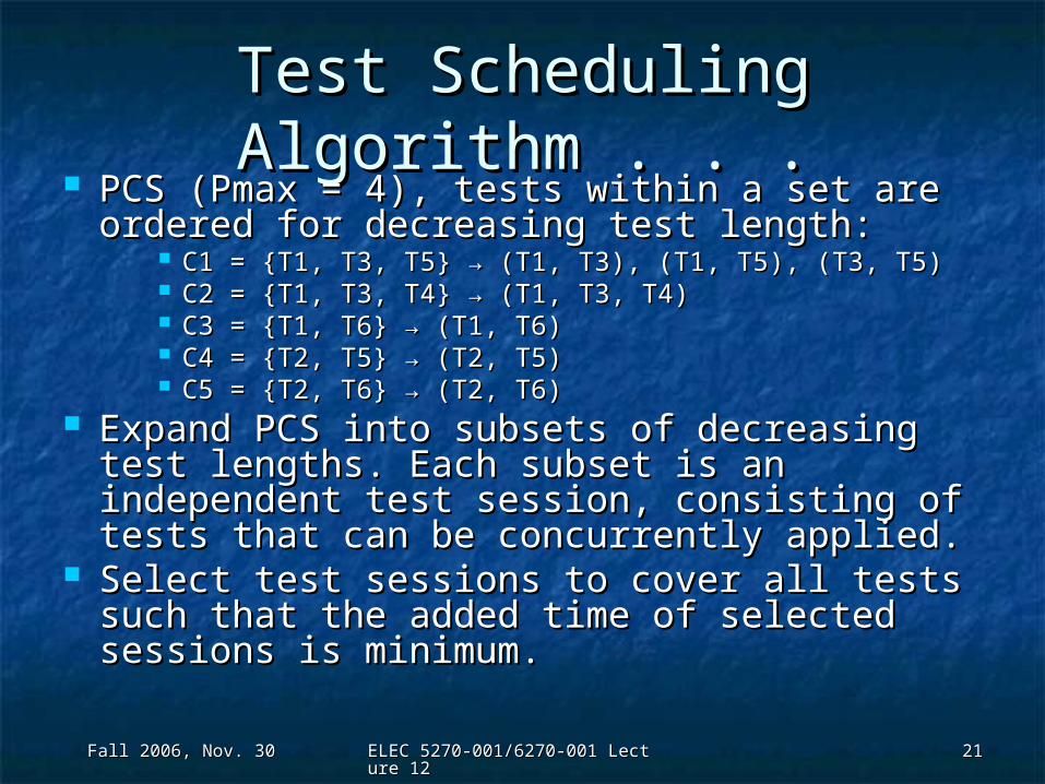
Test Scheduling Test Scheduling Algorithm . . .Algorithm . . .
PCS (Pmax = 4), tests within a set are PCS (Pmax = 4), tests within a set are ordered for decreasing test length:ordered for decreasing test length:
C1 = {T1, T3, T5} → (T1, T3), (T1, T5), (T3, T5)C1 = {T1, T3, T5} → (T1, T3), (T1, T5), (T3, T5) C2 = {T1, T3, T4} → (T1, T3, T4)C2 = {T1, T3, T4} → (T1, T3, T4) C3 = {T1, T6} → (T1, T6)C3 = {T1, T6} → (T1, T6) C4 = {T2, T5} → (T2, T5)C4 = {T2, T5} → (T2, T5) C5 = {T2, T6} → (T2, T6)C5 = {T2, T6} → (T2, T6)
Expand PCS into subsets of decreasing test Expand PCS into subsets of decreasing test lengths. Each subset is an independent test lengths. Each subset is an independent test session, consisting of tests that can be session, consisting of tests that can be concurrently applied.concurrently applied.
Select test sessions to cover all tests such Select test sessions to cover all tests such that the added time of selected sessions is that the added time of selected sessions is minimum.minimum.
Fall 2006, Nov. 30Fall 2006, Nov. 30 ELEC 5270-001/6270-001 Lecture 12ELEC 5270-001/6270-001 Lecture 12 2222
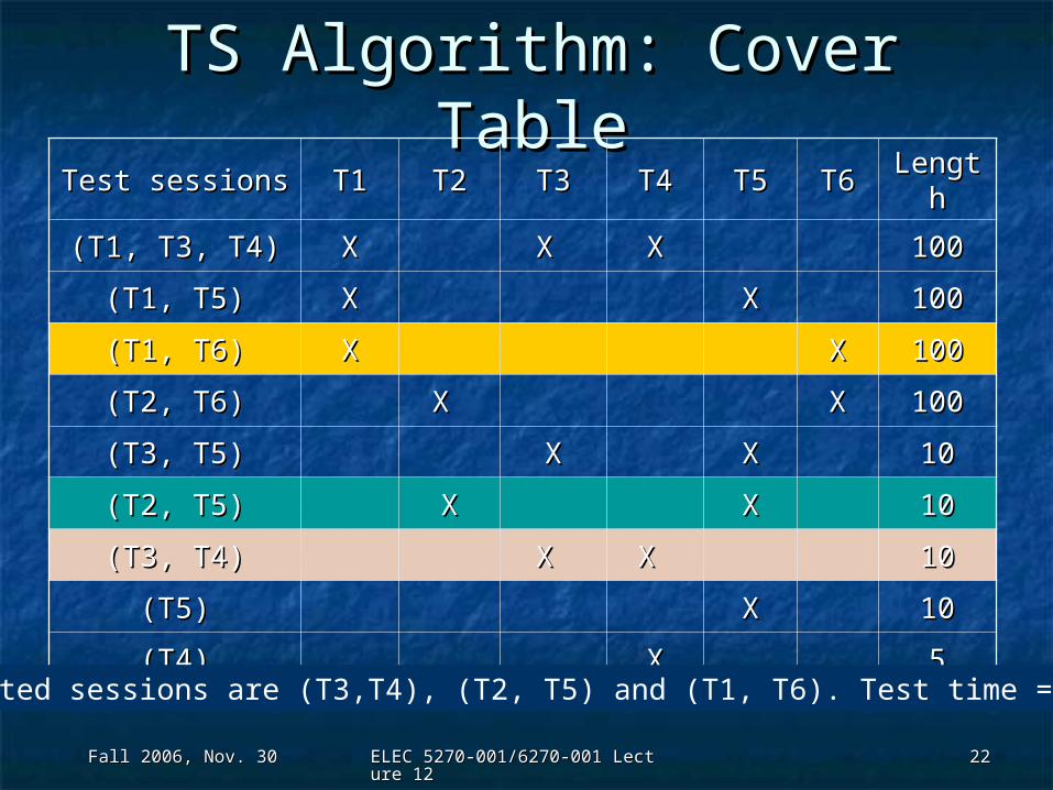
TS Algorithm: Cover TableTS Algorithm: Cover TableTest sessionsTest sessions T1T1 T2T2 T3T3 T4T4 T5T5 T6T6 LengtLengt
hh
(T1, T3, T4)(T1, T3, T4) XX X X XX 100100
(T1, T5)(T1, T5) XX XX 100100
(T1, T6)(T1, T6) XX XX 100100
(T2, T6)(T2, T6) X X XX 100100
(T3, T5)(T3, T5) XX XX 1010
(T2, T5)(T2, T5) XX XX 1010
(T3, T4)(T3, T4) X X X X 1010
(T5)(T5) XX 1010
(T4)(T4) XX 55
Selected sessions are (T3,T4), (T2, T5) and (T1, T6). Test time = 120.
Fall 2006, Nov. 30Fall 2006, Nov. 30 ELEC 5270-001/6270-001 Lecture 12ELEC 5270-001/6270-001 Lecture 12 2323
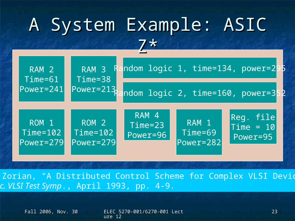
A System Example: ASIC Z*A System Example: ASIC Z*
RAM 2Time=61
Power=241
RAM 3Time=38
Power=213
ROM 1Time=102
Power=279
ROM 2Time=102
Power=279
RAM 1Time=69
Power=282
RAM 4Time=23
Power=96
Reg. fileTime = 10Power=95
Random logic 1, time=134, power=295
Random logic 2, time=160, power=352
*Y. Zorian, “A Distributed Control Scheme for Complex VLSI Devices,” Proc. VLSI Test Symp., April 1993, pp. 4-9.
Fall 2006, Nov. 30Fall 2006, Nov. 30 ELEC 5270-001/6270-001 Lecture 12ELEC 5270-001/6270-001 Lecture 12 2424
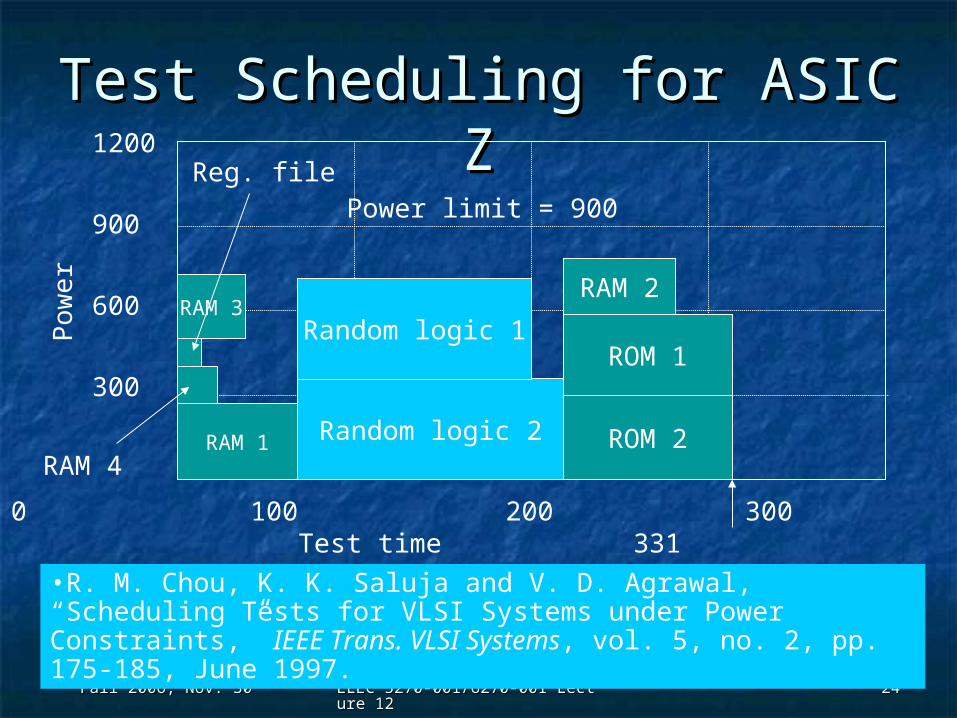
Test Scheduling for ASIC ZTest Scheduling for ASIC Z1200
900
600
300
Po
we
r
Power limit = 900
0 100 200 300 400Test time 331
RAM 1
RAM 3
Random logic 2
Random logic 1
ROM 2
ROM 1
RAM 2
Reg. file
RAM 4
•R. M. Chou, K. K. Saluja and V. D. Agrawal, “Scheduling Tests for VLSI Systems under Power Constraints,” IEEE Trans. VLSI Systems, vol. 5, no. 2, pp. 175-185, June 1997.
Fall 2006, Nov. 30Fall 2006, Nov. 30 ELEC 5270-001/6270-001 Lecture 12ELEC 5270-001/6270-001 Lecture 12 2525
ReferencesReferences
N. Nicolici and B. M. Al-Hashimi, N. Nicolici and B. M. Al-Hashimi, Power-Constrained Testing of VLSI Power-Constrained Testing of VLSI CircuitsCircuits, Boston: Kluwer Academic , Boston: Kluwer Academic Publishers, 2003.Publishers, 2003.
E. Larsson, E. Larsson, Introduction to Advanced Introduction to Advanced System-on-Chip Test Design and System-on-Chip Test Design and OptimizationOptimization, Springer 2005., Springer 2005.