Copyright Agrawal, 2007 ELEC6270 Fall 07, Lecture 3 1 ELEC 5270/6270 Fall 2007 Low-Power Design of...
56
Copyright Agrawal, 2007 Copyright Agrawal, 2007 ELEC6270 Fall 07, Lecture 3 ELEC6270 Fall 07, Lecture 3 1 ELEC 5270/6270 Fall 2007 ELEC 5270/6270 Fall 2007 Low-Power Design of Electronic Low-Power Design of Electronic Circuits Circuits Logic-Level Power Logic-Level Power Estimation Estimation Vishwani D. Agrawal Vishwani D. Agrawal James J. Danaher Professor James J. Danaher Professor Dept. of Electrical and Computer Engineering Dept. of Electrical and Computer Engineering Auburn University, Auburn, AL 36849 Auburn University, Auburn, AL 36849 [email protected] http://www.eng.auburn.edu/~vagrawal/COURSE/E6270_Fall07/ course.html
-
date post
20-Dec-2015 -
Category
Documents
-
view
214 -
download
0
Transcript of Copyright Agrawal, 2007 ELEC6270 Fall 07, Lecture 3 1 ELEC 5270/6270 Fall 2007 Low-Power Design of...

Copyright Agrawal, 2007Copyright Agrawal, 2007 ELEC6270 Fall 07, Lecture 3ELEC6270 Fall 07, Lecture 3 11
ELEC 5270/6270 Fall 2007ELEC 5270/6270 Fall 2007Low-Power Design of Electronic CircuitsLow-Power Design of Electronic Circuits
Logic-Level Power EstimationLogic-Level Power Estimation
Vishwani D. AgrawalVishwani D. AgrawalJames J. Danaher ProfessorJames J. Danaher Professor
Dept. of Electrical and Computer EngineeringDept. of Electrical and Computer EngineeringAuburn University, Auburn, AL 36849Auburn University, Auburn, AL 36849
[email protected]://www.eng.auburn.edu/~vagrawal/COURSE/E6270_Fall07/course.html

Copyright Agrawal, 2007Copyright Agrawal, 2007 ELEC6270 Fall 07, Lecture 3ELEC6270 Fall 07, Lecture 3 22
Power AnalysisPower AnalysisMotivation:Motivation:
SpecificationSpecificationOptimizationOptimizationReliabilityReliability
ApplicationsApplicationsDesign analysis and optimizationDesign analysis and optimizationPhysical designPhysical designPackagingPackagingTestTest
Copyright Agrawal, 2007Copyright Agrawal, 2007 ELEC6270 Fall 07, Lecture 3ELEC6270 Fall 07, Lecture 3 33
Abstraction, Complexity, AccuracyAbstraction, Complexity, Accuracy
Abstraction levelAbstraction level Computing resourcesComputing resources Analysis accuracyAnalysis accuracy
AlgorithmAlgorithm LeastLeast WorstWorst
Software and systemSoftware and system
Hardware behaviorHardware behavior
Register transferRegister transfer
LogicLogic
CircuitCircuit
DeviceDevice MostMost BestBest

Copyright Agrawal, 2007Copyright Agrawal, 2007 ELEC6270 Fall 07, Lecture 3ELEC6270 Fall 07, Lecture 3 44
SpiceSpice Circuit/device level analysisCircuit/device level analysis
Circuit modeled as network of transistors, capacitors, resistors Circuit modeled as network of transistors, capacitors, resistors and voltage/current sources.and voltage/current sources.
Node current equations using Kirchhoff’s current law.Node current equations using Kirchhoff’s current law. Average and instantaneous power computed from supply Average and instantaneous power computed from supply
voltage and device current.voltage and device current.
Analysis is accurate but expensiveAnalysis is accurate but expensive Used to characterize parts of a larger circuit.Used to characterize parts of a larger circuit.
Original references:Original references: L. W. Nagel and D. O. Pederson, “SPICE – Simulation L. W. Nagel and D. O. Pederson, “SPICE – Simulation
Program With Integrated Circuit Emphasis,” Memo ERL-M382, Program With Integrated Circuit Emphasis,” Memo ERL-M382, EECS Dept., University of California, Berkeley, Apr. 1973.EECS Dept., University of California, Berkeley, Apr. 1973.
L. W. Nagel, L. W. Nagel, SPICE 2, A Computer program to Simulate SPICE 2, A Computer program to Simulate Semiconductor CircuitsSemiconductor Circuits, PhD Dissertation, University of , PhD Dissertation, University of California, Berkeley, May 1975.California, Berkeley, May 1975.

Copyright Agrawal, 2007Copyright Agrawal, 2007 ELEC6270 Fall 07, Lecture 3ELEC6270 Fall 07, Lecture 3 55
Ca
Logic Model of MOS CircuitLogic Model of MOS Circuit
Cc
Cb
VDD
a
b
c
pMOS FETs
nMOSFETs
Ca , Cb , Cc and Cd are
node capacitances
Dc
Da ca
b
Da and Db are
interconnect or propagation delays
Dc is inertial delay
of gate
Db
Cd

Copyright Agrawal, 2007Copyright Agrawal, 2007 ELEC6270 Fall 07, Lecture 3ELEC6270 Fall 07, Lecture 3 66
Spice Characterization of a 2-Input Spice Characterization of a 2-Input NAND GateNAND Gate
Input data patternInput data pattern Delay (ps)Delay (ps) Dynamic energy (pJ)Dynamic energy (pJ)
aa = = bb = 0 → 1 = 0 → 1 6969 1.551.55
aa = 1, = 1, bb = 0 → 1 = 0 → 1 6262 1.671.67
a = 0 → 1, b = 1a = 0 → 1, b = 1 5050 1.721.72
aa = = bb = 1 → 0 = 1 → 0 3535 1.821.82
aa = 1, = 1, bb = 1 → 0 = 1 → 0 7676 1.391.39
a = 1 → 0, b = 1a = 1 → 0, b = 1 5757 1.941.94
Copyright Agrawal, 2007Copyright Agrawal, 2007 ELEC6270 Fall 07, Lecture 3ELEC6270 Fall 07, Lecture 3 77
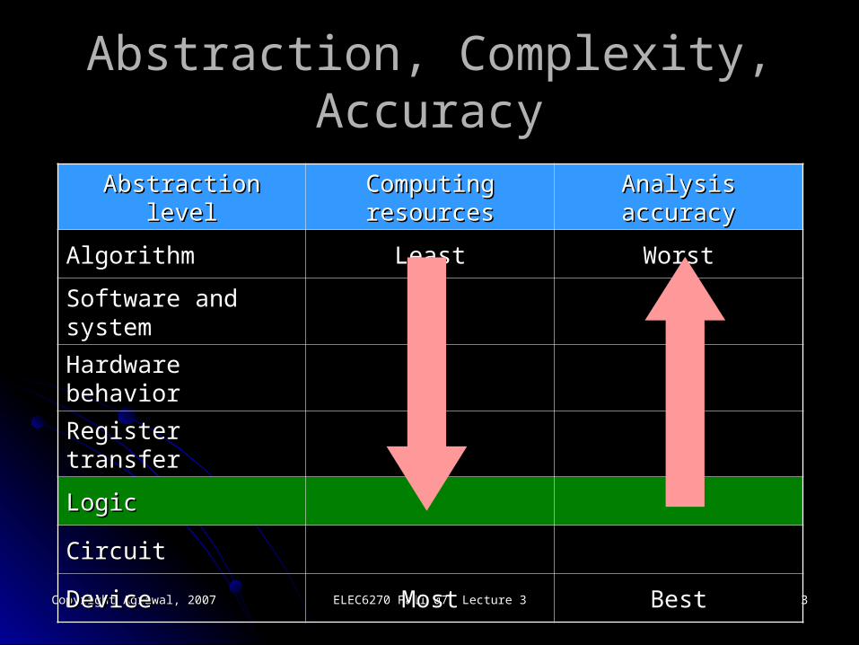
Spice Characterization (Cont.)Spice Characterization (Cont.)
Input data patternInput data pattern Static power (pW)Static power (pW)
aa = = bb = 0 = 0 5.055.05
a = 0, b = 1a = 0, b = 1 13.113.1
aa = 1, = 1, bb = 0 = 0 5.105.10
aa = = bb = 1 = 1 28.528.5

Copyright Agrawal, 2007Copyright Agrawal, 2007 ELEC6270 Fall 07, Lecture 3ELEC6270 Fall 07, Lecture 3 88
Switch-Level PartitioningSwitch-Level Partitioning Circuit partitioned into channel-connected components Circuit partitioned into channel-connected components
for Spice characterization.for Spice characterization. Reference: R. E. Bryant, “A Switch-Level Model and Reference: R. E. Bryant, “A Switch-Level Model and
Simulator for MOS Digital Systems,” Simulator for MOS Digital Systems,” IEEE Trans. IEEE Trans. ComputersComputers, vol. C-33, no. 2, pp. 160-177, Feb. 1984., vol. C-33, no. 2, pp. 160-177, Feb. 1984.
G1
G2
G3
Internal switching nodes not seen by logic simulator

Copyright Agrawal, 2007Copyright Agrawal, 2007 ELEC6270 Fall 07, Lecture 3ELEC6270 Fall 07, Lecture 3 99
Delay and Discrete-Event SimulationDelay and Discrete-Event Simulation (NAND gate)(NAND gate)
b
a
c (CMOS)
Time units 0 5
c (zero delay)
c (unit delay)
c (multiple delay)
c (minmax delay)
Inp
uts
Log
ic s
imul
atio
n
min =2, max =5
rise=5, fall=5
Transient region
Unknown (X)
X

Copyright Agrawal, 2007Copyright Agrawal, 2007 ELEC6270 Fall 07, Lecture 3ELEC6270 Fall 07, Lecture 3 1010
Event-Driven Simulation ExampleEvent-Driven Simulation Example
2
2
4
2
a =1
b =1
c =1→0
d = 0
e =1
f =0
g =1
Time, t 0 4 8
g
t = 0 12345678
Scheduledevents
c = 0
d = 1, e = 0
g = 0
f = 1
g = 1
Activitylist
d, e
f, g
gTim
e s
tack
Copyright Agrawal, 2007Copyright Agrawal, 2007 ELEC6270 Fall 07, Lecture 3ELEC6270 Fall 07, Lecture 3 1111
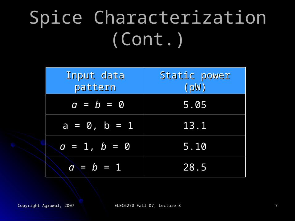
Time Wheel (Circular Stack)Time Wheel (Circular Stack)
t=0
1
2
3
4
5
6
7
maxCurrenttimepointer Event link-list

Copyright Agrawal, 2007Copyright Agrawal, 2007 ELEC6270 Fall 07, Lecture 3ELEC6270 Fall 07, Lecture 3 1212
Gate-Level Power AnalysisGate-Level Power AnalysisPre-simulation analysis:Pre-simulation analysis:
Partition circuit into channel connected gate Partition circuit into channel connected gate components.components.
Determine node capacitances from layout Determine node capacitances from layout analysis (accurate) or from wire-load model* analysis (accurate) or from wire-load model* (approximate).(approximate).
Determine dynamic and static power from Spice Determine dynamic and static power from Spice for each gate.for each gate.
Determine gate delays using Spice or Elmore Determine gate delays using Spice or Elmore delay model.delay model.
* Wire-load model estimates capacitance of a net by its pin-count. See Yeap, p. 39.

Copyright Agrawal, 2007Copyright Agrawal, 2007 ELEC6270 Fall 07, Lecture 3ELEC6270 Fall 07, Lecture 3 1313
Elmore Delay ModelElmore Delay Model W. Elmore, “The Transient Response of Damped Linear Networks W. Elmore, “The Transient Response of Damped Linear Networks
with Particular Regard to Wideband Amplifiers,” with Particular Regard to Wideband Amplifiers,” J. Appl. PhysJ. Appl. Phys., vol. ., vol. 19, no.1, pp. 55-63, Jan. 1948.19, no.1, pp. 55-63, Jan. 1948.
s 1
2
3
4
5
R1
R2
R3
R4
R5
C1
C2
C3
C5
C4
Shared resistance:
R45 = R1 + R3R15 = R1R34 = R1 + R3
Copyright Agrawal, 2007Copyright Agrawal, 2007 ELEC6270 Fall 07, Lecture 3ELEC6270 Fall 07, Lecture 3 1414
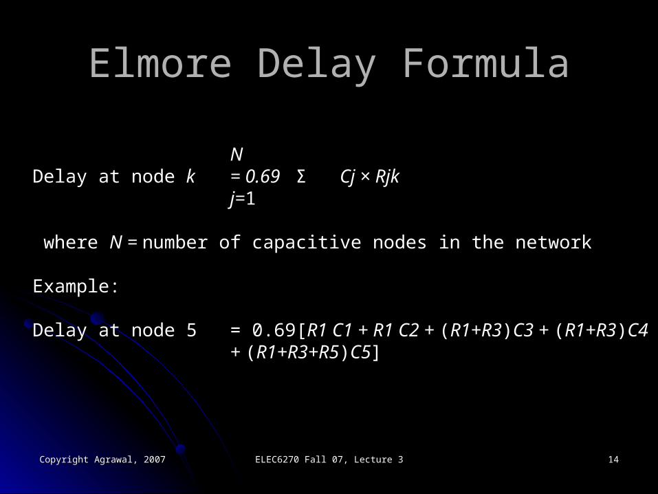
Elmore Delay FormulaElmore Delay Formula
NDelay at node k = 0.69 Σ Cj × Rjk
j=1
where N = number of capacitive nodes in the network
Example:
Delay at node 5 = 0.69[R1 C1 + R1 C2 + (R1+R3)C3 + (R1+R3)C4 + (R1+R3+R5)C5]
Copyright Agrawal, 2007Copyright Agrawal, 2007 ELEC6270 Fall 07, Lecture 3ELEC6270 Fall 07, Lecture 3 1515
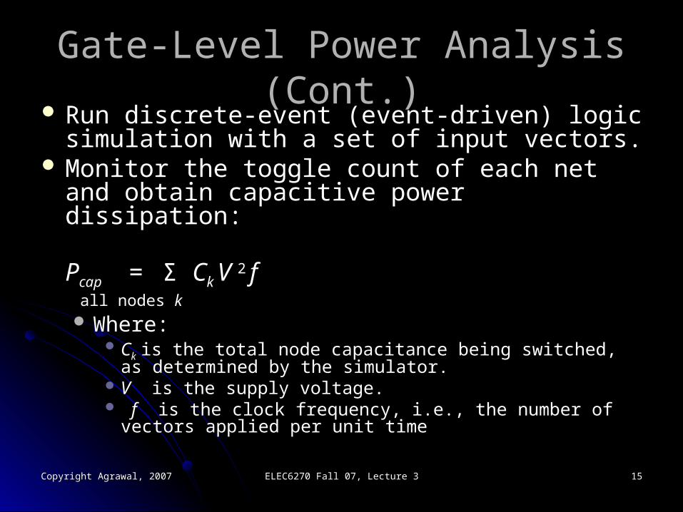
Gate-Level Power Analysis (Cont.)Gate-Level Power Analysis (Cont.) Run discrete-event (event-driven) logic Run discrete-event (event-driven) logic
simulation with a set of input vectors.simulation with a set of input vectors. Monitor the toggle count of each net and obtain Monitor the toggle count of each net and obtain
capacitive power dissipation:capacitive power dissipation:
PPcapcap == ΣΣ CCk k V V 22 ff all nodes all nodes kk
Where:Where: CCkk is the total node capacitance being switched, as is the total node capacitance being switched, as
determined by the simulator.determined by the simulator. VV is the supply voltage. is the supply voltage. ff is the clock frequency, i.e., the number of vectors applied is the clock frequency, i.e., the number of vectors applied
per unit timeper unit time

Copyright Agrawal, 2007Copyright Agrawal, 2007 ELEC6270 Fall 07, Lecture 3ELEC6270 Fall 07, Lecture 3 1616
Gate-Level Power Analysis (Cont.)Gate-Level Power Analysis (Cont.)
Monitor dynamic energy events at the input Monitor dynamic energy events at the input of each gate and obtain internal switching of each gate and obtain internal switching power dissipation:power dissipation:
PPintint = = ΣΣ ΣΣ E(g,e) F(g,e)E(g,e) F(g,e) gates gates g g events events ee
WhereWhereE(g,e) = E(g,e) = energy of event energy of event ee of gate of gate gg, pre-computed , pre-computed
from Spice.from Spice.F(g,e) = F(g,e) = occurrence frequency of the eventoccurrence frequency of the event e e at gateat gate
g, g, observed by logic simulationobserved by logic simulation..

Copyright Agrawal, 2007Copyright Agrawal, 2007 ELEC6270 Fall 07, Lecture 3ELEC6270 Fall 07, Lecture 3 1717
Gate-Level Power Analysis (Cont.)Gate-Level Power Analysis (Cont.)
Monitor the static power dissipation state of each Monitor the static power dissipation state of each gate and obtain the static power dissipation:gate and obtain the static power dissipation:
PPstatstat = = ΣΣ ΣΣ P(g,s) T(g,s)/ TP(g,s) T(g,s)/ T gates gates gg states states ss
WhereWhere P(g,s) = P(g,s) = static power dissipation of gatestatic power dissipation of gate g g for statefor state s, s,
obtained from Spiceobtained from Spice.. T(g,s) = T(g,s) = duration of stateduration of state s s at gateat gate g, g, obtained from logic obtained from logic
simulationsimulation.. T = T = vector periodvector period..
Copyright Agrawal, 2007Copyright Agrawal, 2007 ELEC6270 Fall 07, Lecture 3ELEC6270 Fall 07, Lecture 3 1818
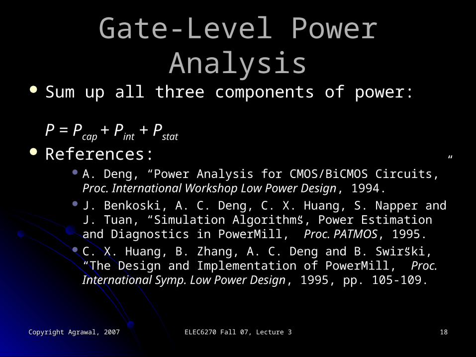
Gate-Level Power AnalysisGate-Level Power Analysis Sum up all three components of power:Sum up all three components of power:
P = PP = Pcap cap + P+ Pintint + P + Pstatstat
References:References: A. Deng, “Power Analysis for CMOS/BiCMOS Circuits,” A. Deng, “Power Analysis for CMOS/BiCMOS Circuits,” Proc. Proc.
International Workshop Low Power DesignInternational Workshop Low Power Design, 1994., 1994. J. Benkoski, A. C. Deng, C. X. Huang, S. Napper and J. Tuan, J. Benkoski, A. C. Deng, C. X. Huang, S. Napper and J. Tuan,
“Simulation Algorithms, Power Estimation and Diagnostics in “Simulation Algorithms, Power Estimation and Diagnostics in PowerMill,” PowerMill,” Proc. PATMOSProc. PATMOS, 1995., 1995.
C. X. Huang, B. Zhang, A. C. Deng and B. Swirski, “The Design C. X. Huang, B. Zhang, A. C. Deng and B. Swirski, “The Design and Implementation of PowerMill,” and Implementation of PowerMill,” Proc. International Symp. Low Proc. International Symp. Low Power DesignPower Design, 1995, pp. 105-109., 1995, pp. 105-109.

Copyright Agrawal, 2007Copyright Agrawal, 2007 ELEC6270 Fall 07, Lecture 3ELEC6270 Fall 07, Lecture 3 1919
Probabilistic AnalysisProbabilistic Analysis
View signals as a random processesView signals as a random processes
Prob{s(t) = 1} = p1 p0 = 1 – p1
C
0→1 transition probability = (1 – p1) p1
Power, P = (1 – p1) p1 CV2fck

Copyright Agrawal, 2007Copyright Agrawal, 2007 ELEC6270 Fall 07, Lecture 3ELEC6270 Fall 07, Lecture 3 2020
Source of InaccuracySource of Inaccuracy
1/fck
p1 = 0.5 P = 0.5CV 2 fck
p1 = 0.5 P = 0.33CV 2 fck
p1 = 0.5 P = 0.167CV 2 fck
Observe that the formula, Power, P = (1 – p1) p1 C V 2 fck , is notCorrect.
Copyright Agrawal, 2007Copyright Agrawal, 2007 ELEC6270 Fall 07, Lecture 3ELEC6270 Fall 07, Lecture 3 2121
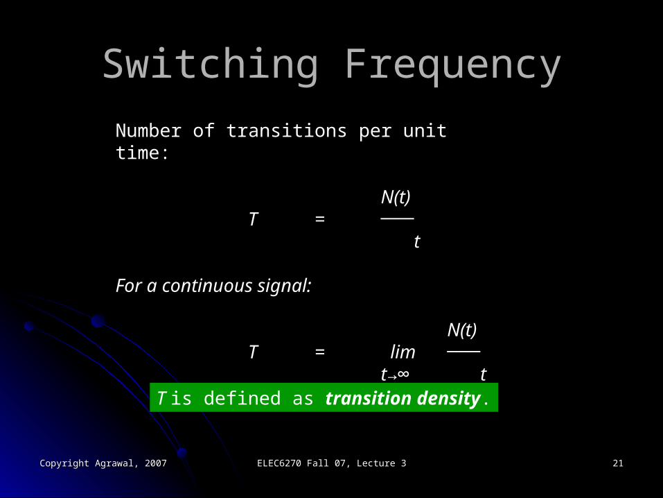
Switching FrequencySwitching Frequency
Number of transitions per unit time:
N(t)T = ───
t
For a continuous signal:
N(t)T = lim ───
t→∞ t
T is defined as transition density.

Copyright Agrawal, 2007Copyright Agrawal, 2007 ELEC6270 Fall 07, Lecture 3ELEC6270 Fall 07, Lecture 3 2222
Static Signal ProbabilitiesStatic Signal Probabilities
Observe signal for interval Observe signal for interval t t 0 + 0 + t t 11Signal is 1 for duration Signal is 1 for duration t t 11Signal is 0 for duration Signal is 0 for duration t t 00Signal probabilities:Signal probabilities:
p p 1 = 1 = t t 1/(1/(t t 0 + 0 + t t 1)1) p p 0 = 0 = t t 0/(0/(t t 0 + 0 + t t 1) = 1 – 1) = 1 – p p 11

Copyright Agrawal, 2007Copyright Agrawal, 2007 ELEC6270 Fall 07, Lecture 3ELEC6270 Fall 07, Lecture 3 2323
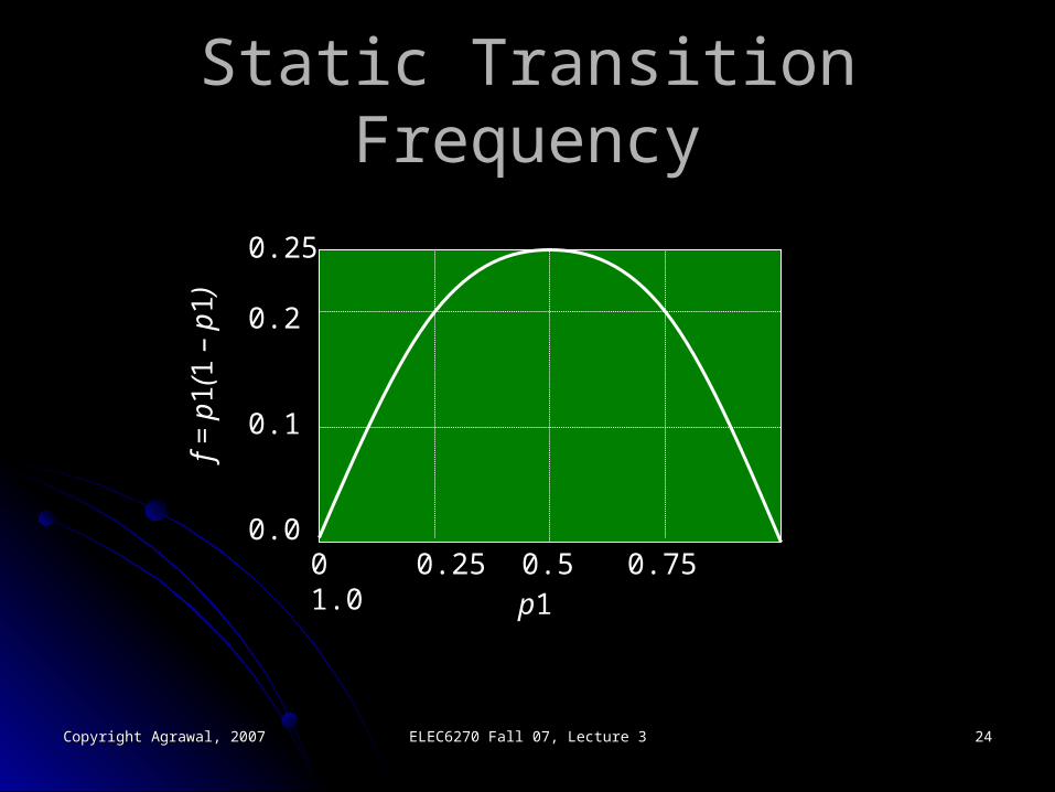
Static Transition ProbabilitiesStatic Transition Probabilities
Transition probabilities:Transition probabilities: T T 01 = 01 = p p 0 Prob{signal is 1 | signal was 0} = 0 Prob{signal is 1 | signal was 0} = p p 0 0 pp11 T T 10 = 10 = p p 1 Prob{signal is 0 | signal was 1} = 1 Prob{signal is 0 | signal was 1} = p p 1 1 p p 00 TT = = T T 01 + 01 + T T 10 = 2 10 = 2 p p 0 0 p p 1 = 2 1 = 2 p p 1 (1 – 1 (1 – p p 1)1)
Transition density: Transition density: TT = 2 = 2 p p 1 (1 – 1 (1 – p p 1)1)
Copyright Agrawal, 2007Copyright Agrawal, 2007 ELEC6270 Fall 07, Lecture 3ELEC6270 Fall 07, Lecture 3 2424
Static Transition FrequencyStatic Transition Frequency
0 0.25 0.5 0.75 1.0
0.25
0.2
0.1
0.0
p1
f =
p1
(1 –
p1
)
Copyright Agrawal, 2007Copyright Agrawal, 2007 ELEC6270 Fall 07, Lecture 3ELEC6270 Fall 07, Lecture 3 2525
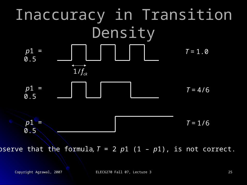
Inaccuracy in Transition DensityInaccuracy in Transition Density
1/fck
p1 = 0.5 T = 1.0
p1 = 0.5 T = 4/6
p1 = 0.5 T = 1/6
Observe that the formula, T = 2 p1 (1 – p1), is not correct.

Copyright Agrawal, 2007Copyright Agrawal, 2007 ELEC6270 Fall 07, Lecture 3ELEC6270 Fall 07, Lecture 3 2626
Cause for Error and CorrectionCause for Error and CorrectionProbability of transition is not independent of Probability of transition is not independent of
the present state of the signal.the present state of the signal.Determine probability Determine probability p p 01 of a 0→1 01 of a 0→1
transition.transition.Recognize Recognize p p 01 ≠ 01 ≠ p p 0 × 0 × p p 11We obtain We obtain p p 1 = (1 – 1 = (1 – p p 1)1)p p 01 + 01 + p p 1 1 p p 1111
p p 0101p p 1 = ─────────1 = ─────────
1 – 1 – p p 11 + 11 + p p 0101

Copyright Agrawal, 2007Copyright Agrawal, 2007 ELEC6270 Fall 07, Lecture 3ELEC6270 Fall 07, Lecture 3 2727
Correction (Cont.)Correction (Cont.) Since Since p p 11 + 11 + p p 10 = 1, i.e., given that the 10 = 1, i.e., given that the
signal was previously 1, its present value can signal was previously 1, its present value can be either 1 or 0.be either 1 or 0.
Therefore,Therefore, p p 0101
p p 1 = ──────1 = ────── p p 10 + 10 + p p 0101
This uniquely gives signal probability as a This uniquely gives signal probability as a function of transition probabilities.function of transition probabilities.
Copyright Agrawal, 2007Copyright Agrawal, 2007 ELEC6270 Fall 07, Lecture 3ELEC6270 Fall 07, Lecture 3 2828
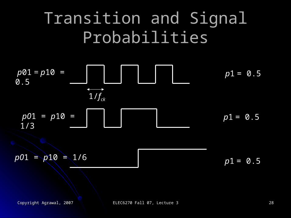
Transition and Signal ProbabilitiesTransition and Signal Probabilities
1/fck
p01 = p10 = 0.5 p1 = 0.5
p01 = p10 = 1/3 p1 = 0.5
p1 = 0.5p01 = p10 = 1/6

Copyright Agrawal, 2007Copyright Agrawal, 2007 ELEC6270 Fall 07, Lecture 3ELEC6270 Fall 07, Lecture 3 2929
Probabilities: p0, p1, p00, p01, p10, p11Probabilities: p0, p1, p00, p01, p10, p11
p p 01 + 01 + p p 00 =100 =1 p p 11 + 11 + p p 10 = 110 = 1 p p 0 = 1 – 0 = 1 – p p 11
p p 0101
p p 1 = ───────1 = ───────
p p 10 + 10 + p p 0101

Copyright Agrawal, 2007Copyright Agrawal, 2007 ELEC6270 Fall 07, Lecture 3ELEC6270 Fall 07, Lecture 3 3030
Transition DensityTransition Density
TT = 2 = 2 p p 1 (1 – 1 (1 – p p 1) = 1) = p p 0 0 p p 01 + 01 + p p 1 1 p p 1010
= 2 = 2 p p 10 10 p p 01 / (01 / (p p 10 + 10 + p p 01)01)
= 2 = 2 p p 1 1 p p 10 = 2 10 = 2 p p 0 0 p p 0101

Copyright Agrawal, 2007Copyright Agrawal, 2007 ELEC6270 Fall 07, Lecture 3ELEC6270 Fall 07, Lecture 3 3131
Power CalculationPower Calculation
Power can be estimated if transition Power can be estimated if transition density is known for all signals.density is known for all signals.
Calculation of transition density requiresCalculation of transition density requiresSignal probabilitiesSignal probabilitiesTransition densities for primary inputs; Transition densities for primary inputs;
computed from vector statisticscomputed from vector statistics

Copyright Agrawal, 2007Copyright Agrawal, 2007 ELEC6270 Fall 07, Lecture 3ELEC6270 Fall 07, Lecture 3 3232
Signal ProbabilitiesSignal Probabilities
x1
x2
x1 x2
x1
x2
x1 + x2 – x1x2
x1 1 - x1

Copyright Agrawal, 2007Copyright Agrawal, 2007 ELEC6270 Fall 07, Lecture 3ELEC6270 Fall 07, Lecture 3 3333
Signal ProbabilitiesSignal Probabilities x1
x2 x3
x1 x2
y = 1 - (1 - x1x2) x3 = 1 - x3 + x1x2x3 = 0.625
X1 X2 X3 Y0 0 0 10 0 1 00 1 0 10 1 1 01 0 0 11 0 1 01 1 0 11 1 1 1
0.5
0.5
0.5
0.25 0.625
Ref: K. P. Parker and E. J. McCluskey,“Probabilistic Treatment of General Combinational Networks,” IEEE Trans. on Computers, vol. C-24, no. 6, pp. 668-670, June 1975.

Copyright Agrawal, 2007Copyright Agrawal, 2007 ELEC6270 Fall 07, Lecture 3ELEC6270 Fall 07, Lecture 3 3434
Correlated Signal ProbabilitiesCorrelated Signal Probabilities
x1
x2
x1 x2
y = 1 - (1 - x1x2) x2 = 1 – x2 + x1x2x2 = 1 – x2 + x1x2 = 0.75 (correct value)
X1 X2 Y0 0 10 1 01 0 11 1 1
0.5
0.5 0.25 0.625?

Copyright Agrawal, 2007Copyright Agrawal, 2007 ELEC6270 Fall 07, Lecture 3ELEC6270 Fall 07, Lecture 3 3535
Correlated Signal ProbabilitiesCorrelated Signal Probabilities
x1
x2
x1 + x2 – x1x2
y = (x1 + x2 – x1x2) x2 = x1x2 + x2x2 – x1x2x2 = x1x2 + x2 – x1x2 = x2 = 0.5 (correct value)
X1 X2 Y0 0 00 1 11 0 01 1 1
0.5
0.5 0.75 0.375?

Copyright Agrawal, 2007Copyright Agrawal, 2007 ELEC6270 Fall 07, Lecture 3ELEC6270 Fall 07, Lecture 3 3636
ObservationObservation
Numerical computation of signal Numerical computation of signal probabilities is accurate for fanout-free probabilities is accurate for fanout-free circuits.circuits.

Copyright Agrawal, 2007Copyright Agrawal, 2007 ELEC6270 Fall 07, Lecture 3ELEC6270 Fall 07, Lecture 3 3737
RemediesRemedies
Use Shannon’s expansion theorem to Use Shannon’s expansion theorem to compute signal probabilities.compute signal probabilities.
Use Boolean difference formula to Use Boolean difference formula to compute transition densities.compute transition densities.
Copyright Agrawal, 2007Copyright Agrawal, 2007 ELEC6270 Fall 07, Lecture 3ELEC6270 Fall 07, Lecture 3 3838
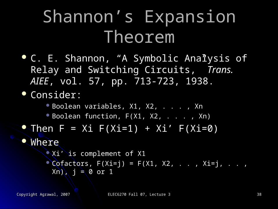
Shannon’s Expansion TheoremShannon’s Expansion Theorem
C. E. Shannon, “A Symbolic Analysis of Relay C. E. Shannon, “A Symbolic Analysis of Relay and Switching Circuits,” and Switching Circuits,” Trans. AIEETrans. AIEE, vol. 57, , vol. 57, pp. 713-723, 1938.pp. 713-723, 1938.
Consider:Consider: Boolean variables, X1, X2, . . . , XnBoolean variables, X1, X2, . . . , Xn Boolean function, F(X1, X2, . . . , Xn)Boolean function, F(X1, X2, . . . , Xn)
Then F = Xi F(Xi=1) + Xi’ F(Xi=0)Then F = Xi F(Xi=1) + Xi’ F(Xi=0) WhereWhere
Xi’ is complement of X1Xi’ is complement of X1 Cofactors, F(Xi=j) = F(X1, X2, . . , Xi=j, . . , Xn), j = 0 or 1Cofactors, F(Xi=j) = F(X1, X2, . . , Xi=j, . . , Xn), j = 0 or 1
Copyright Agrawal, 2007Copyright Agrawal, 2007 ELEC6270 Fall 07, Lecture 3ELEC6270 Fall 07, Lecture 3 3939
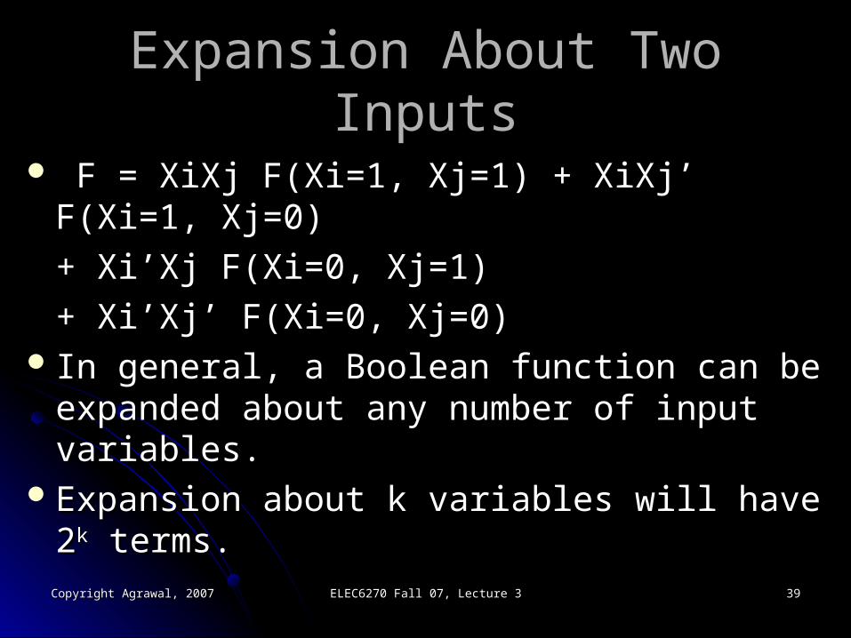
Expansion About Two InputsExpansion About Two Inputs
F = XiXj F(Xi=1, Xj=1) + XiXj’ F(Xi=1, Xj=0)F = XiXj F(Xi=1, Xj=1) + XiXj’ F(Xi=1, Xj=0)
+ Xi’Xj F(Xi=0, Xj=1)+ Xi’Xj F(Xi=0, Xj=1)
+ Xi’Xj’ F(Xi=0, Xj=0)+ Xi’Xj’ F(Xi=0, Xj=0) In general, a Boolean function can be In general, a Boolean function can be
expanded about any number of input expanded about any number of input variables.variables.
Expansion about k variables will have 2Expansion about k variables will have 2kk terms.terms.

Copyright Agrawal, 2007Copyright Agrawal, 2007 ELEC6270 Fall 07, Lecture 3ELEC6270 Fall 07, Lecture 3 4040
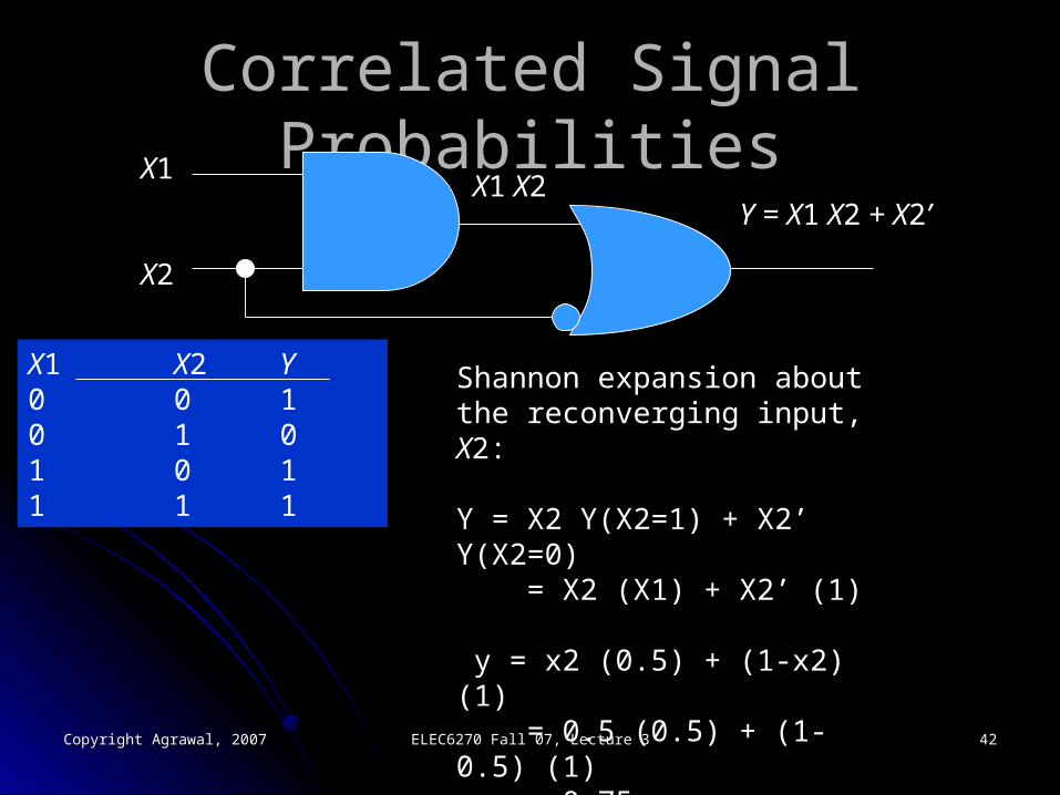
Correlated Signal ProbabilitiesCorrelated Signal Probabilities
X1
X2
X1 X2
X1 X2 Y0 0 10 1 01 0 11 1 1
Y = X1 X2 + X2’
Shannon expansion about the reconverging input, X2:
Y = X2 Y(X2 = 1) + X2’ Y(X2 = 0) = X2 (X1) + X2’ (1)

Copyright Agrawal, 2007Copyright Agrawal, 2007 ELEC6270 Fall 07, Lecture 3ELEC6270 Fall 07, Lecture 3 4141
Correlated SignalsCorrelated Signals
When the output function is expanded about all When the output function is expanded about all reconverging input variables,reconverging input variables,
All cofactors correspond to fanout-free circuits.All cofactors correspond to fanout-free circuits. Signal probabilities for cofactor outputs can be calculated Signal probabilities for cofactor outputs can be calculated
without error.without error. A weighted sum of cofactor probabilities gives the correct A weighted sum of cofactor probabilities gives the correct
probability of the output.probability of the output.
For two reconverging inputs:For two reconverging inputs:
f = xixj f(Xi=1, Xj=1) + xi(1-xj) f(Xi=1, Xj=0)f = xixj f(Xi=1, Xj=1) + xi(1-xj) f(Xi=1, Xj=0)
+ (1-xi)xj f(Xi=0, Xj=1) + (1-xi)(1-xj) f(Xi=0, Xj=0)+ (1-xi)xj f(Xi=0, Xj=1) + (1-xi)(1-xj) f(Xi=0, Xj=0)
Copyright Agrawal, 2007Copyright Agrawal, 2007 ELEC6270 Fall 07, Lecture 3ELEC6270 Fall 07, Lecture 3 4242
Correlated Signal ProbabilitiesCorrelated Signal Probabilities X1
X2
X1 X2
X1 X2 Y0 0 10 1 01 0 11 1 1
Y = X1 X2 + X2’
Shannon expansion about the reconverging input, X2:
Y = X2 Y(X2=1) + X2’ Y(X2=0) = X2 (X1) + X2’ (1)
y = x2 (0.5) + (1-x2) (1) = 0.5 (0.5) + (1-0.5) (1) = 0.75

Copyright Agrawal, 2007Copyright Agrawal, 2007 ELEC6270 Fall 07, Lecture 3ELEC6270 Fall 07, Lecture 3 4343
ExampleExample
Point of reconv.
Supergate0.5
0.5
0.5
0.5
0.25
10
0.50.0
0.01.0
0.51.0
Signal probability for supergate output = 0.5 Prob{rec. signal = 1} + 1.0 Prob{rec. signal = 0} = 0.5 × 0.5 + 1.0 × 0.5 = 0.75
0.375
Reconv. signal
S. C. Seth and V. D. Agrawal, “A New Model for Computation ofProbabilistic Testability in Combinational Circuits,” Integration, the VLSI Journal, vol. 7, no. 1, pp. 49-75, April 1989.
Copyright Agrawal, 2007Copyright Agrawal, 2007 ELEC6270 Fall 07, Lecture 3ELEC6270 Fall 07, Lecture 3 4444
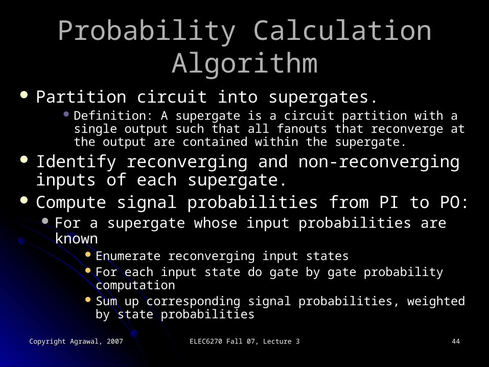
Probability Calculation AlgorithmProbability Calculation Algorithm
Partition circuit into supergates.Partition circuit into supergates. Definition: A supergate is a circuit partition with a single output Definition: A supergate is a circuit partition with a single output
such that all fanouts that reconverge at the output are contained such that all fanouts that reconverge at the output are contained within the supergate. within the supergate.
Identify reconverging and non-reconverging inputs Identify reconverging and non-reconverging inputs of each supergate.of each supergate.
Compute signal probabilities from PI to PO:Compute signal probabilities from PI to PO: For a supergate whose input probabilities are knownFor a supergate whose input probabilities are known
Enumerate reconverging input statesEnumerate reconverging input states For each input state do gate by gate probability computationFor each input state do gate by gate probability computation Sum up corresponding signal probabilities, weighted by state Sum up corresponding signal probabilities, weighted by state
probabilitiesprobabilities

Copyright Agrawal, 2007Copyright Agrawal, 2007 ELEC6270 Fall 07, Lecture 3ELEC6270 Fall 07, Lecture 3 4545
Calculating Transition DensityCalculating Transition Density
Boolean function
1
n
x1, T1..... xn, Tn
y, T(Y) = ?

Copyright Agrawal, 2007Copyright Agrawal, 2007 ELEC6270 Fall 07, Lecture 3ELEC6270 Fall 07, Lecture 3 4646
Boolean DifferenceBoolean Difference
Boolean diff(Y, Xi) = 1 means that a path is sensitized from input Boolean diff(Y, Xi) = 1 means that a path is sensitized from input Xi to output Y.Xi to output Y.
Prob(Boolean diff(Y, Xi) = 1) is the probability of transmitting a Prob(Boolean diff(Y, Xi) = 1) is the probability of transmitting a toggle from Xi to Y.toggle from Xi to Y.
Probability of Boolean difference is determined from the Probability of Boolean difference is determined from the probabilities of cofactors of Y with respect to Xi. probabilities of cofactors of Y with respect to Xi.
∂YBoolean diff(Y, Xi) = ── = Y(Xi=1) ⊕ Y(Xi=0)
∂Xi
F. F. Sellers, M. Y. Hsiao and L. W. Bearnson, “Analyzing Errors with the Boolean Difference,” IEEE Trans. on Computers, vol. C-17, no. 7, pp. 676-683, July 1968.
Copyright Agrawal, 2007Copyright Agrawal, 2007 ELEC6270 Fall 07, Lecture 3ELEC6270 Fall 07, Lecture 3 4747
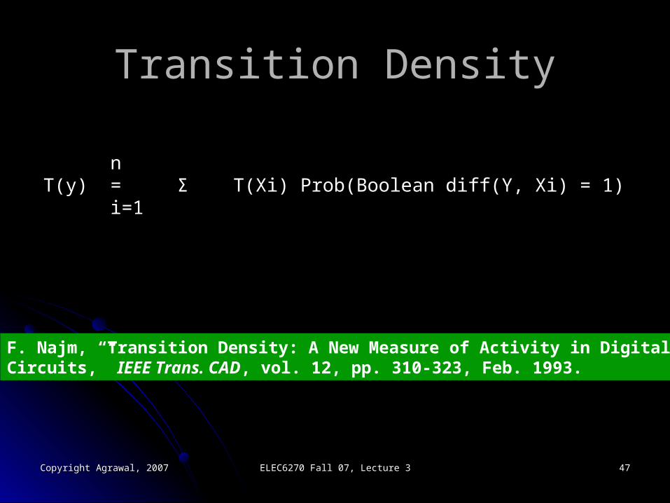
Transition DensityTransition Density
nT(y) = Σ T(Xi) Prob(Boolean diff(Y, Xi) = 1)
i=1
F. Najm, “Transition Density: A New Measure of Activity in DigitalCircuits,” IEEE Trans. CAD, vol. 12, pp. 310-323, Feb. 1993.
Copyright Agrawal, 2007Copyright Agrawal, 2007 ELEC6270 Fall 07, Lecture 3ELEC6270 Fall 07, Lecture 3 4848
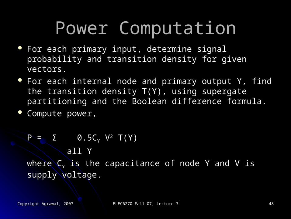
Power ComputationPower Computation For each primary input, determine signal probability and For each primary input, determine signal probability and
transition density for given vectors.transition density for given vectors. For each internal node and primary output Y, find the For each internal node and primary output Y, find the
transition density T(Y), using supergate partitioning and transition density T(Y), using supergate partitioning and the Boolean difference formula.the Boolean difference formula.
Compute power,Compute power,
P =P = ΣΣ 0.5C0.5CYY V V22 T(Y) T(Y)
all Yall Y
where Cwhere CYY is the capacitance of node Y and V is supply is the capacitance of node Y and V is supply
voltage.voltage.

Copyright Agrawal, 2007Copyright Agrawal, 2007 ELEC6270 Fall 07, Lecture 3ELEC6270 Fall 07, Lecture 3 4949
Transition Density and PowerTransition Density and Power
X1
X2 X3
0.2, 1
0.3, 2
0.4, 3
0.06, 0.7
0.436, 3.24
Transition densitySignal probability
YCi
CY
Power = 0.5 V 2 (0.7Ci + 3.24CY)

Copyright Agrawal, 2007Copyright Agrawal, 2007 ELEC6270 Fall 07, Lecture 3ELEC6270 Fall 07, Lecture 3 5050
Prob. Method vs. Logic Sim. Prob. Method vs. Logic Sim.
CircuitCircuit No. of No. of gatesgates
Probability methodProbability method Logic SimulationLogic SimulationErrorError
%%Av. densityAv. density CPU s*CPU s* Av. densityAv. density CPU s*CPU s*
C432C432 160160 3.463.46 0.520.52 3.393.39 6363 +2.1+2.1
C499C499 202202 11.3611.36 0.580.58 8.578.57 241241 +29.8+29.8
C880C880 383383 2.782.78 1.061.06 3.253.25 132132 -14.5-14.5
C1355C1355 346346 4.194.19 1.391.39 6.186.18 408408 -32.2-32.2
C1908C1908 880880 2.972.97 2.002.00 5.015.01 464464 -40.7-40.7
C2670C2670 11931193 3.503.50 3.453.45 4.004.00 619619 -12.5-12.5
C3540C3540 16691669 4.474.47 3.773.77 4.494.49 10821082 -0.4-0.4
C5315C5315 23072307 3.523.52 6.416.41 4.794.79 16161616 -26.5-26.5
C6288C6288 24062406 25.1025.10 5.675.67 34.1734.17 3105731057 -26.5-26.5
C7552C7552 35123512 3.833.83 9.859.85 5.085.08 27132713 -24.2-24.2* CONVEX c240
Copyright Agrawal, 2007Copyright Agrawal, 2007 ELEC6270 Fall 07, Lecture 3ELEC6270 Fall 07, Lecture 3 5151
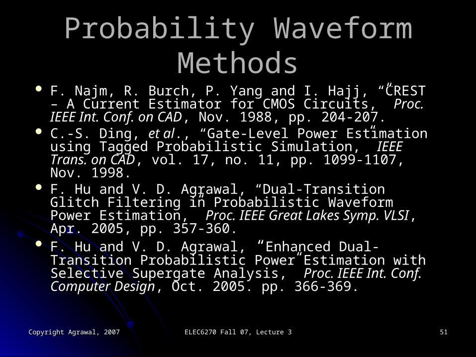
Probability Waveform MethodsProbability Waveform Methods F. Najm, R. Burch, P. Yang and I. Hajj, “CREST – A F. Najm, R. Burch, P. Yang and I. Hajj, “CREST – A
Current Estimator for CMOS Circuits,” Current Estimator for CMOS Circuits,” Proc. IEEE Int. Proc. IEEE Int. Conf. on CADConf. on CAD, Nov. 1988, pp. 204-207., Nov. 1988, pp. 204-207.
C.-S. Ding, C.-S. Ding, et alet al., “Gate-Level Power Estimation using ., “Gate-Level Power Estimation using Tagged Probabilistic Simulation,” Tagged Probabilistic Simulation,” IEEE Trans. on CADIEEE Trans. on CAD, , vol. 17, no. 11, pp. 1099-1107, Nov. 1998.vol. 17, no. 11, pp. 1099-1107, Nov. 1998.
F. Hu and V. D. Agrawal, “Dual-Transition Glitch Filtering F. Hu and V. D. Agrawal, “Dual-Transition Glitch Filtering in Probabilistic Waveform Power Estimation,” in Probabilistic Waveform Power Estimation,” Proc. IEEE Proc. IEEE Great Lakes Symp. VLSIGreat Lakes Symp. VLSI, Apr. 2005, pp. 357-360., Apr. 2005, pp. 357-360.
F. Hu and V. D. Agrawal,F. Hu and V. D. Agrawal, “ “Enhanced Dual-Transition Enhanced Dual-Transition Probabilistic Power Estimation with Selective Supergate Probabilistic Power Estimation with Selective Supergate Analysis,” Analysis,” Proc. IEEE Int. Conf. Computer DesignProc. IEEE Int. Conf. Computer Design, Oct. , Oct. 2005. pp. 366-369.2005. pp. 366-369.
Copyright Agrawal, 2007Copyright Agrawal, 2007 ELEC6270 Fall 07, Lecture 3ELEC6270 Fall 07, Lecture 3 5252
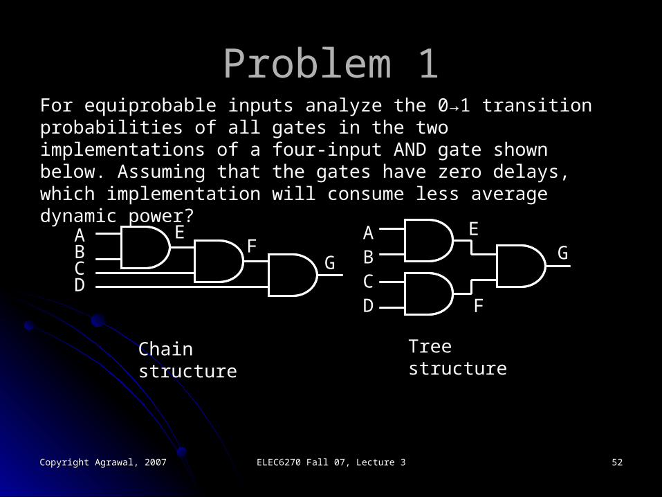
Problem 1Problem 1For equiprobable inputs analyze the 0→1 transition probabilities of all gates in the two implementations of a four-input AND gate shown below. Assuming that the gates have zero delays, which implementation will consume less average dynamic power?
Chain structure Tree structure
ABCD
EF
G
ABCD
E
F
G

Copyright Agrawal, 2007Copyright Agrawal, 2007 ELEC6270 Fall 07, Lecture 3ELEC6270 Fall 07, Lecture 3 5353
Problem 1 SolutionProblem 1 SolutionGiven the primary input probabilities, P(A) = P(B) = P(C) = P(D) = 0.5, signal and transition (0→1) probabilities are as follows:
Signalname
Chain Tree
Prob(sig.= 1) Prob(0→1) Prob(sig.=1) Prob(0→1)
E 0.2500 0.1875 0.2500 0.1875
F 0.1250 0.1094 0.2500 0.1875
G 0.0625 0.0586 0.0625 0.0586
Total transitions/vector
0.3555 0.4336
The tree implementation consumes 100×(0.4336 – 0.3555)/0.3555 = 22% more average dynamic power. This advantage of the chain structure may be somewhat reduced because of glitches caused by unbalanced path delays.

Copyright Agrawal, 2007Copyright Agrawal, 2007 ELEC6270 Fall 07, Lecture 3ELEC6270 Fall 07, Lecture 3 5454
Problem 2Problem 2Assume that the two-input AND gates in Problem 1 each has one unit of delay. Find input vector pairs for each implementation that will consume the peak dynamic power. Which implementation consumes less peak dynamic power?
Chain structure Tree structure
ABCD
EF
G
ABCD
E
F
G

Copyright Agrawal, 2007Copyright Agrawal, 2007 ELEC6270 Fall 07, Lecture 3ELEC6270 Fall 07, Lecture 3 5555
Problem 2 SolutionProblem 2 SolutionFor the chain structure, a vector pair {A B C D} = {1110},{1011} will produce four gate transitions as shown below.
A
BCD
EF
G
A=11
B=10
E=10
C=11
F=10
D=01
G=00
Time units0 1 2 3

Copyright Agrawal, 2007Copyright Agrawal, 2007 ELEC6270 Fall 07, Lecture 3ELEC6270 Fall 07, Lecture 3 5656
Problem 2 Solution (Cont.)Problem 2 Solution (Cont.)The tree structure has balanced delay paths. So it cannot make more than 3 gate transitions. A vector pair {ABCD} = {1111},{1010} will produce three transitions as shown below.
A
B
C
D
E
F
G
A=11
B=10
E=10
C=11
D=10
F=10
G=10Time units
0 1 2 3
Therefore, just counting the gate transitions, we find that the chain consumes 100(4 – 3)/3 = 33% higher peak power than the tree.
![Radiometry and Reflectance: From Terminology Concepts to ...docs.fct.unesp.br/docentes/carto/enner/PPGCC...[18:16 27/2/2009 5270-Warner-Ch15.tex] Paper Size: a4 paper Job No: 5270](https://static.fdocuments.in/doc/165x107/607434d9c04595405c48cb35/radiometry-and-reiectance-from-terminology-concepts-to-docsfctunespbrdocentescartoennerppgcc.jpg)