Fall 2006, Sep. 26, Oct. 3 ELEC 5270-001/6270-001 Lecture 7 1 ELEC 5270-001/6270-001(Fall 2006)...
46
Fall 2006, Sep. 26, Fall 2006, Sep. 26, Oct. 3 Oct. 3 ELEC 5270-001/6270-001 Lect ELEC 5270-001/6270-001 Lect ure 7 ure 7 1 ELEC 5270-001/6270-001(Fall ELEC 5270-001/6270-001(Fall 2006) 2006) Low-Power Design of Electronic Circuits Low-Power Design of Electronic Circuits Dynamic Power: Glitch Elimination Dynamic Power: Glitch Elimination Vishwani D. Agrawal Vishwani D. Agrawal James J. Danaher Professor James J. Danaher Professor Department of Electrical and Computer Department of Electrical and Computer Engineering Engineering Auburn University, Auburn, AL 36849 Auburn University, Auburn, AL 36849 http://www.eng.auburn.edu/~vagrawal http://www.eng.auburn.edu/~vagrawal [email protected] [email protected]
-
date post
21-Dec-2015 -
Category
Documents
-
view
217 -
download
2
Transcript of Fall 2006, Sep. 26, Oct. 3 ELEC 5270-001/6270-001 Lecture 7 1 ELEC 5270-001/6270-001(Fall 2006)...

Fall 2006, Sep. 26, Oct. 3Fall 2006, Sep. 26, Oct. 3 ELEC 5270-001/6270-001 Lecture 7ELEC 5270-001/6270-001 Lecture 7 11
ELEC 5270-001/6270-001(Fall ELEC 5270-001/6270-001(Fall 2006)2006)
Low-Power Design of Electronic CircuitsLow-Power Design of Electronic Circuits
Dynamic Power: Glitch EliminationDynamic Power: Glitch Elimination
Vishwani D. AgrawalVishwani D. AgrawalJames J. Danaher ProfessorJames J. Danaher Professor
Department of Electrical and Computer Department of Electrical and Computer EngineeringEngineering
Auburn University, Auburn, AL 36849Auburn University, Auburn, AL 36849http://www.eng.auburn.edu/~vagrawalhttp://www.eng.auburn.edu/~vagrawal
[email protected]@eng.auburn.edu

Fall 2006, Sep. 26, Oct. 3Fall 2006, Sep. 26, Oct. 3 ELEC 5270-001/6270-001 Lecture 7ELEC 5270-001/6270-001 Lecture 7 22
Components of PowerComponents of Power
DynamicDynamic Signal transitionsSignal transitions
Logic activityLogic activity GlitchesGlitches
Short-circuitShort-circuit StaticStatic
LeakageLeakage

Fall 2006, Sep. 26, Oct. 3Fall 2006, Sep. 26, Oct. 3 ELEC 5270-001/6270-001 Lecture 7ELEC 5270-001/6270-001 Lecture 7 33
Power of a TransitionPower of a Transition
VVDDDD
GroundGround
CL
R
R
Dynamic Power
= CLVDD2/2 + Psc
Vi
Vo
isc
Fall 2006, Sep. 26, Oct. 3Fall 2006, Sep. 26, Oct. 3 ELEC 5270-001/6270-001 Lecture 7ELEC 5270-001/6270-001 Lecture 7 44
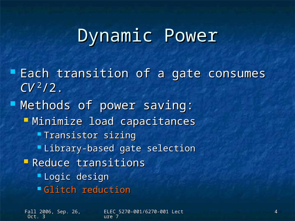
Dynamic PowerDynamic Power
Each transition of a gate consumes Each transition of a gate consumes CV CV 22/2./2.
Methods of power saving:Methods of power saving: Minimize load capacitancesMinimize load capacitances
Transistor sizingTransistor sizing Library-based gate selectionLibrary-based gate selection
Reduce transitionsReduce transitions Logic designLogic design Glitch reductionGlitch reduction

Fall 2006, Sep. 26, Oct. 3Fall 2006, Sep. 26, Oct. 3 ELEC 5270-001/6270-001 Lecture 7ELEC 5270-001/6270-001 Lecture 7 55
Glitch Power ReductionGlitch Power Reduction Design a digital circuit for minimum Design a digital circuit for minimum
transient energy consumption by transient energy consumption by eliminating hazardseliminating hazards

Fall 2006, Sep. 26, Oct. 3Fall 2006, Sep. 26, Oct. 3 ELEC 5270-001/6270-001 Lecture 7ELEC 5270-001/6270-001 Lecture 7 66
Theorem 1Theorem 1 For correct operation with For correct operation with
minimum energy consumption, a minimum energy consumption, a Boolean gate must produce no Boolean gate must produce no more than more than oneone event per transition. event per transition.
Output logic state changesOne transition is necessary
Output logic state unchangedNo transition is necessary

Fall 2006, Sep. 26, Oct. 3Fall 2006, Sep. 26, Oct. 3 ELEC 5270-001/6270-001 Lecture 7ELEC 5270-001/6270-001 Lecture 7 77
Event PropagationEvent Propagation
2 4 61
1 3
5
3
10
0
0
2
2
Path P1
P2
Path P3
Single lumped inertial delay modeled for each gatePI transitions assumed to occur without time skew

Fall 2006, Sep. 26, Oct. 3Fall 2006, Sep. 26, Oct. 3 ELEC 5270-001/6270-001 Lecture 7ELEC 5270-001/6270-001 Lecture 7 88
Inertial Delay of an InverterInertial Delay of an Inverter
dHL dLH
dHL+dLH
d = ──── 2
Vin
Vout
time

Fall 2006, Sep. 26, Oct. 3Fall 2006, Sep. 26, Oct. 3 ELEC 5270-001/6270-001 Lecture 7ELEC 5270-001/6270-001 Lecture 7 99
Multi-Input GateMulti-Input Gate
Delay = d
A
B
C
A
B
C d d Hazard or glitch
DPD

Fall 2006, Sep. 26, Oct. 3Fall 2006, Sep. 26, Oct. 3 ELEC 5270-001/6270-001 Lecture 7ELEC 5270-001/6270-001 Lecture 7 1010
Balanced Path DelaysBalanced Path Delays
Delay = d
A
B
C
A
B
C d No glitch
DPD

Fall 2006, Sep. 26, Oct. 3Fall 2006, Sep. 26, Oct. 3 ELEC 5270-001/6270-001 Lecture 7ELEC 5270-001/6270-001 Lecture 7 1111
Glitch Filtering by InertiaGlitch Filtering by Inertia
Delay ≥ DPD
A
B
C
A
B
C
d =DPD
Filtered glitch
DPD
Fall 2006, Sep. 26, Oct. 3Fall 2006, Sep. 26, Oct. 3 ELEC 5270-001/6270-001 Lecture 7ELEC 5270-001/6270-001 Lecture 7 1212
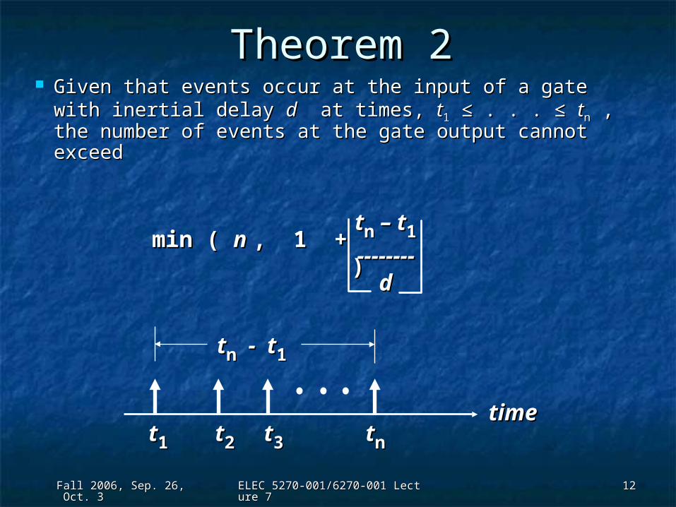
Given that events occur at the input of a gate with Given that events occur at the input of a gate with inertial delay inertial delay dd at times, at times, tt11 ≤ . . . ≤ ≤ . . . ≤ ttnn , the number , the number of events at the gate output cannot exceedof events at the gate output cannot exceed
Theorem 2Theorem 2
min ( min ( n n , 1 + ), 1 + )ttnn – t – t11
----------------dd
ttnn - t - t11
tt11 t t22 t t33 t tnn timetime

Fall 2006, Sep. 26, Oct. 3Fall 2006, Sep. 26, Oct. 3 ELEC 5270-001/6270-001 Lecture 7ELEC 5270-001/6270-001 Lecture 7 1313
Minimum Transient DesignMinimum Transient Design
Minimum transient energy condition for a Minimum transient energy condition for a Boolean gate:Boolean gate:
| t| tii - t - tjj | < d | < d
Where tWhere tii and t and tjj are arrival times of input are arrival times of input
events and d is the inertial delay of gateevents and d is the inertial delay of gate

Fall 2006, Sep. 26, Oct. 3Fall 2006, Sep. 26, Oct. 3 ELEC 5270-001/6270-001 Lecture 7ELEC 5270-001/6270-001 Lecture 7 1414
Balanced Delay MethodBalanced Delay Method All input events arrive simultaneouslyAll input events arrive simultaneously Overall circuit delay not increasedOverall circuit delay not increased Delay buffers may have to be insertedDelay buffers may have to be inserted
11 111111 11
111111
33
11 11
No increase in critical path delay

Fall 2006, Sep. 26, Oct. 3Fall 2006, Sep. 26, Oct. 3 ELEC 5270-001/6270-001 Lecture 7ELEC 5270-001/6270-001 Lecture 7 1515
Hazard Filter MethodHazard Filter Method Gate delay is made greater than maximum input Gate delay is made greater than maximum input
path delay differencepath delay difference No delay buffers needed No delay buffers needed (least transient energy)(least transient energy) Overall circuit delay may increaseOverall circuit delay may increase
11 111111 11
33111111 11

Fall 2006, Sep. 26, Oct. 3Fall 2006, Sep. 26, Oct. 3 ELEC 5270-001/6270-001 Lecture 7ELEC 5270-001/6270-001 Lecture 7 1616
Linear ProgramLinear Program
Variables: gate and buffer delaysVariables: gate and buffer delays Objective: minimize number of buffersObjective: minimize number of buffers Subject to: overall circuit delay Subject to: overall circuit delay
constraint for all input-output pathsconstraint for all input-output paths Subject to: minimum transient Subject to: minimum transient
condition for all multi-input gatescondition for all multi-input gates

Fall 2006, Sep. 26, Oct. 3Fall 2006, Sep. 26, Oct. 3 ELEC 5270-001/6270-001 Lecture 7ELEC 5270-001/6270-001 Lecture 7 1717
Variables for Full Adder Variables for Full Adder add1badd1b
1111
11 11
1111
11
11
11
0000
00
0000
00
00 0000
0000
00
00

Fall 2006, Sep. 26, Oct. 3Fall 2006, Sep. 26, Oct. 3 ELEC 5270-001/6270-001 Lecture 7ELEC 5270-001/6270-001 Lecture 7 1818
Variables for Full Adder Variables for Full Adder add1badd1b
Gate delay variables dGate delay variables d4 4 . . . d. . . d1212 Buffer delay variables dBuffer delay variables d15 15 . . . . . .
dd2929
Fall 2006, Sep. 26, Oct. 3Fall 2006, Sep. 26, Oct. 3 ELEC 5270-001/6270-001 Lecture 7ELEC 5270-001/6270-001 Lecture 7 1919
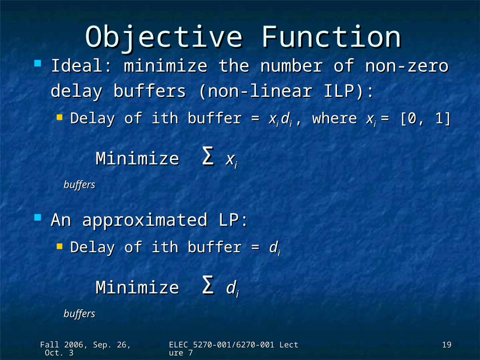
Objective FunctionObjective Function Ideal: minimize the number of non-zero Ideal: minimize the number of non-zero
delay buffers (non-linear ILP):delay buffers (non-linear ILP): Delay of ith buffer = Delay of ith buffer = xxi i ddi i , , where where xxi i = [0, 1]= [0, 1]
Minimize Minimize ΣΣ xxi i buffersbuffers
An approximated LP:An approximated LP: Delay of ith buffer = Delay of ith buffer = ddii
Minimize Minimize ΣΣ ddi i buffersbuffers

Fall 2006, Sep. 26, Oct. 3Fall 2006, Sep. 26, Oct. 3 ELEC 5270-001/6270-001 Lecture 7ELEC 5270-001/6270-001 Lecture 7 2020
Specify Critical Path DelaySpecify Critical Path Delay
1111
11 11
1111
11
11
11
0000
00
0000
00
00 0000
0000
00
00
Sum of delays on critical path ≤ Sum of delays on critical path ≤ maxdelmaxdel maxdel = specified critical path delaymaxdel = specified critical path delay

Fall 2006, Sep. 26, Oct. 3Fall 2006, Sep. 26, Oct. 3 ELEC 5270-001/6270-001 Lecture 7ELEC 5270-001/6270-001 Lecture 7 2121
Multi-Input Gate ConditionMulti-Input Gate Condition
11
11 11
11
0000
00
0000
00
d1d1
d2d2
dd
d1 - d2 ≤ dd1 - d2 ≤ dd2 - d1 ≤ dd2 - d1 ≤ d
dd
dd
|d1 - d2| ≤ d ≡|d1 - d2| ≤ d ≡

Fall 2006, Sep. 26, Oct. 3Fall 2006, Sep. 26, Oct. 3 ELEC 5270-001/6270-001 Lecture 7ELEC 5270-001/6270-001 Lecture 7 2222
Results: 1-Bit AdderResults: 1-Bit Adder
Fall 2006, Sep. 26, Oct. 3Fall 2006, Sep. 26, Oct. 3 ELEC 5270-001/6270-001 Lecture 7ELEC 5270-001/6270-001 Lecture 7 2323
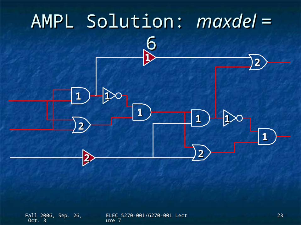
AMPL Solution: AMPL Solution: maxdel maxdel == 66
2211
11 11
1111
22
11
22
22
11

Fall 2006, Sep. 26, Oct. 3Fall 2006, Sep. 26, Oct. 3 ELEC 5270-001/6270-001 Lecture 7ELEC 5270-001/6270-001 Lecture 7 2424
AMPL Solution: AMPL Solution: maxdel maxdel == 77
2222
11 11
1111
11
11
33
22

Fall 2006, Sep. 26, Oct. 3Fall 2006, Sep. 26, Oct. 3 ELEC 5270-001/6270-001 Lecture 7ELEC 5270-001/6270-001 Lecture 7 2525
AMPL Solution: AMPL Solution: maxdel maxdel ≥≥ 1111
2233
11 11
1111
44
33
55

Fall 2006, Sep. 26, Oct. 3Fall 2006, Sep. 26, Oct. 3 ELEC 5270-001/6270-001 Lecture 7ELEC 5270-001/6270-001 Lecture 7 2626
Original 1-Bit AdderOriginal 1-Bit Adder
Colo
r co
des
for
num
ber
of
transi
tions

Fall 2006, Sep. 26, Oct. 3Fall 2006, Sep. 26, Oct. 3 ELEC 5270-001/6270-001 Lecture 7ELEC 5270-001/6270-001 Lecture 7 2727
Optimized 1-Bit AdderOptimized 1-Bit Adder
Colo
r co
des
for
num
ber
of
transi
tions

Fall 2006, Sep. 26, Oct. 3Fall 2006, Sep. 26, Oct. 3 ELEC 5270-001/6270-001 Lecture 7ELEC 5270-001/6270-001 Lecture 7 2828
Results: 1-Bit AdderResults: 1-Bit AdderSimulated over all possible vector transitions
•Average power = optimized/unit delay
= 244 / 308 = 0.792
•Peak power = optimized/unit delay
= 6 / 10 = 0.60
Power Savings :
Peak = 40 %
Average = 21 %

Fall 2006, Sep. 26, Oct. 3Fall 2006, Sep. 26, Oct. 3 ELEC 5270-001/6270-001 Lecture 7ELEC 5270-001/6270-001 Lecture 7 2929
ReferencesReferences E. Jacobs and M. Berkelaar, “Using Gate Sizing to Reduce E. Jacobs and M. Berkelaar, “Using Gate Sizing to Reduce
Glitch Power,” Glitch Power,” Proc. ProRISC/IEEE Workshop on Circuits, Proc. ProRISC/IEEE Workshop on Circuits, Systems and Signal ProcessingSystems and Signal Processing, Nov. 1996, pp. 183-188; , Nov. 1996, pp. 183-188; also also Int. Workshop on Logic SynthesisInt. Workshop on Logic Synthesis, May 1997., May 1997.
V. D. Agrawal, “Low-Power Design by Hazard Filtering,” V. D. Agrawal, “Low-Power Design by Hazard Filtering,” Proc. 10th Int. Conf. VLSI DesignProc. 10th Int. Conf. VLSI Design, Jan. 1997, pp. 193-197., Jan. 1997, pp. 193-197.
V. D. Agrawal, M. L. Bushnell, G. Parthasarathy, and R. V. D. Agrawal, M. L. Bushnell, G. Parthasarathy, and R. Ramadoss, “Digital Circuit Design for Minimum Transient Ramadoss, “Digital Circuit Design for Minimum Transient Energy and a Linear Programming Method,” Energy and a Linear Programming Method,” Proc. 12th Proc. 12th Int. Conf. VLSI DesignInt. Conf. VLSI Design, Jan. 1999, pp. 434-439., Jan. 1999, pp. 434-439.
Last two papers are available at website Last two papers are available at website http://www.eng.auburn.edu/~vagrawalhttp://www.eng.auburn.edu/~vagrawal

Fall 2006, Sep. 26, Oct. 3Fall 2006, Sep. 26, Oct. 3 ELEC 5270-001/6270-001 Lecture 7ELEC 5270-001/6270-001 Lecture 7 3030
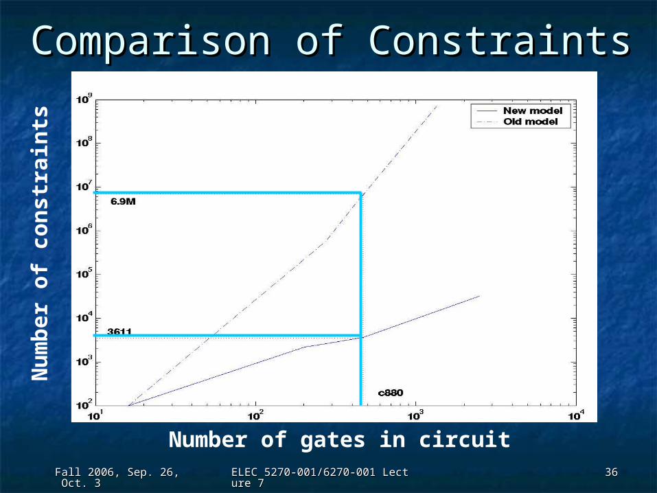
A LimitationA Limitation
Constraints are written by Constraints are written by path path
enumeration.enumeration. Since number of paths in a circuit can be Since number of paths in a circuit can be
exponential in circuit size, the exponential in circuit size, the
formulation is infeasible for large circuits.formulation is infeasible for large circuits. Example: c880 has 6.96M constraints.Example: c880 has 6.96M constraints.

Fall 2006, Sep. 26, Oct. 3Fall 2006, Sep. 26, Oct. 3 ELEC 5270-001/6270-001 Lecture 7ELEC 5270-001/6270-001 Lecture 7 3131
Timing WindowTiming Window Define two Define two timing windowtiming window variablesvariables per per
gate output:gate output: ttii Earliest time of signal transition at gate i. Earliest time of signal transition at gate i.
TTii Latest time of signal transition at gate i. Latest time of signal transition at gate i.t1, T1
tn, Tn
.
.
.
ti, Ti
Ref: T. Raja, Master’s Thesis, Rutgers Univ., 2002
i

Fall 2006, Sep. 26, Oct. 3Fall 2006, Sep. 26, Oct. 3 ELEC 5270-001/6270-001 Lecture 7ELEC 5270-001/6270-001 Lecture 7 3232
Linear ProgramLinear Program
Gate variables dGate variables d4 4 . . . d. . . d1212 Buffer Variables dBuffer Variables d15 15 . . . d. . . d2929 Corresponding window variables tCorresponding window variables t4 4 . . . t. . . t2929 and T and T4 4 . . . . T. . . . T2929..

Fall 2006, Sep. 26, Oct. 3Fall 2006, Sep. 26, Oct. 3 ELEC 5270-001/6270-001 Lecture 7ELEC 5270-001/6270-001 Lecture 7 3333
Multiple-Input Gate ConstraintsMultiple-Input Gate Constraints
For Gate 7:For Gate 7:
TT77 ≥ ≥ TT55 + d + d77;; t t77 < t < t55 + d + d77;; dd77 > T > T77 - t - t77;;
TT77 ≥≥ T T66 + d + d77;; t t77 < t < t66 + d + d77;;

Fall 2006, Sep. 26, Oct. 3Fall 2006, Sep. 26, Oct. 3 ELEC 5270-001/6270-001 Lecture 7ELEC 5270-001/6270-001 Lecture 7 3434
Single-Input Gate Single-Input Gate ConstraintsConstraints
T16 + d19 = T19 ;
t16 + d19 = t19 ;
Buffer 19:
Fall 2006, Sep. 26, Oct. 3Fall 2006, Sep. 26, Oct. 3 ELEC 5270-001/6270-001 Lecture 7ELEC 5270-001/6270-001 Lecture 7 3535
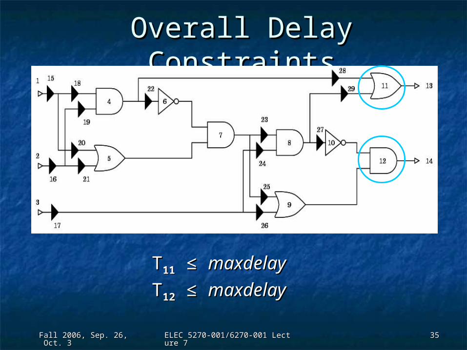
Overall Delay ConstraintsOverall Delay Constraints
TT1111 ≤≤ maxdelaymaxdelay
TT1212 ≤≤ maxdelaymaxdelay
Fall 2006, Sep. 26, Oct. 3Fall 2006, Sep. 26, Oct. 3 ELEC 5270-001/6270-001 Lecture 7ELEC 5270-001/6270-001 Lecture 7 3636
Comparison of ConstraintsComparison of Constraints
Number of gates in circuit
Nu
mb
er o
f co
nst
rain
ts

Fall 2006, Sep. 26, Oct. 3Fall 2006, Sep. 26, Oct. 3 ELEC 5270-001/6270-001 Lecture 7ELEC 5270-001/6270-001 Lecture 7 3737
Estimation of PowerEstimation of Power Circuit is simulated by an event-Circuit is simulated by an event-
driven simulator for both optimized driven simulator for both optimized and un-optimized gate delays.and un-optimized gate delays.
All transitions at a gate are counted All transitions at a gate are counted as Events[gate].as Events[gate].
Power consumed Power consumed Events[gate] x Events[gate] x # of fanouts.# of fanouts.
Ref: “Effects of delay model on peak Ref: “Effects of delay model on peak power estimation of VLSI circuits,” power estimation of VLSI circuits,” Hsiao, Hsiao, et alet al. (. (ICCAD`97 ICCAD`97 ).).

Fall 2006, Sep. 26, Oct. 3Fall 2006, Sep. 26, Oct. 3 ELEC 5270-001/6270-001 Lecture 7ELEC 5270-001/6270-001 Lecture 7 3838
Results: 4-Bit ALUResults: 4-Bit ALU
maxdelaymaxdelay Buffers insertedBuffers inserted
77 55
1010 22
1212 11
1515 00
Power Savings :
Peak = 33 %, Average = 21 %

Fall 2006, Sep. 26, Oct. 3Fall 2006, Sep. 26, Oct. 3 ELEC 5270-001/6270-001 Lecture 7ELEC 5270-001/6270-001 Lecture 7 3939
Power Calculation in SpicePower Calculation in SpiceVDDVDD
GroundGround
CircuitLarge C
Open at t = 0
Ref.: M. Shoji, CMOS Digital Circuit Technology, Prentice Hall, 1988, p. 172.
t
En
erg
y,
E(t
)E(t) = -- C VDD 2 - -- C V 2 ~ C VDD ( VDD - V )
1 1
2 2
V

Fall 2006, Sep. 26, Oct. 3Fall 2006, Sep. 26, Oct. 3 ELEC 5270-001/6270-001 Lecture 7ELEC 5270-001/6270-001 Lecture 7 4040
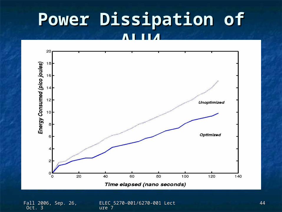
Power Dissipation of ALU4Power Dissipation of ALU4E
ner
gy
in n
an
ojo
ule
s
0
1
2
3
4
5
6
7
0.0 0.5 1.0 1.5 2.0microseconds
Original ALUdelay ~ 3.5ns
Minimum energy ALUdelay ~ 10ns
1 micron CMOS, 57 gates, 14 PI, 8 PO100 random vectors simulated in Spice

Fall 2006, Sep. 26, Oct. 3Fall 2006, Sep. 26, Oct. 3 ELEC 5270-001/6270-001 Lecture 7ELEC 5270-001/6270-001 Lecture 7 4141
F0 Output of ALU4F0 Output of ALU4S
ign
al A
mp
litu
de
, Vo
lts
0
5
0 40 80 120 160nanoseconds
Original ALU, delay = 7 units (~3.5ns)
Minimum energy ALU, delay = 21 units (~10ns)
5
0

Fall 2006, Sep. 26, Oct. 3Fall 2006, Sep. 26, Oct. 3 ELEC 5270-001/6270-001 Lecture 7ELEC 5270-001/6270-001 Lecture 7 4242
Benchmark CircuitsBenchmark CircuitsCircuit
C432
C880
C6288
c7552
Maxdel.(gates)
1734
2448
4794
4386
No. ofBuffers
9566
6234
294120
366111
Average
0.720.62
0.680.68
0.400.36
0.380.36
Peak
0.670.60
0.540.52
0.360.34
0.340.32
Normalized Power
Fall 2006, Sep. 26, Oct. 3Fall 2006, Sep. 26, Oct. 3 ELEC 5270-001/6270-001 Lecture 7ELEC 5270-001/6270-001 Lecture 7 4343
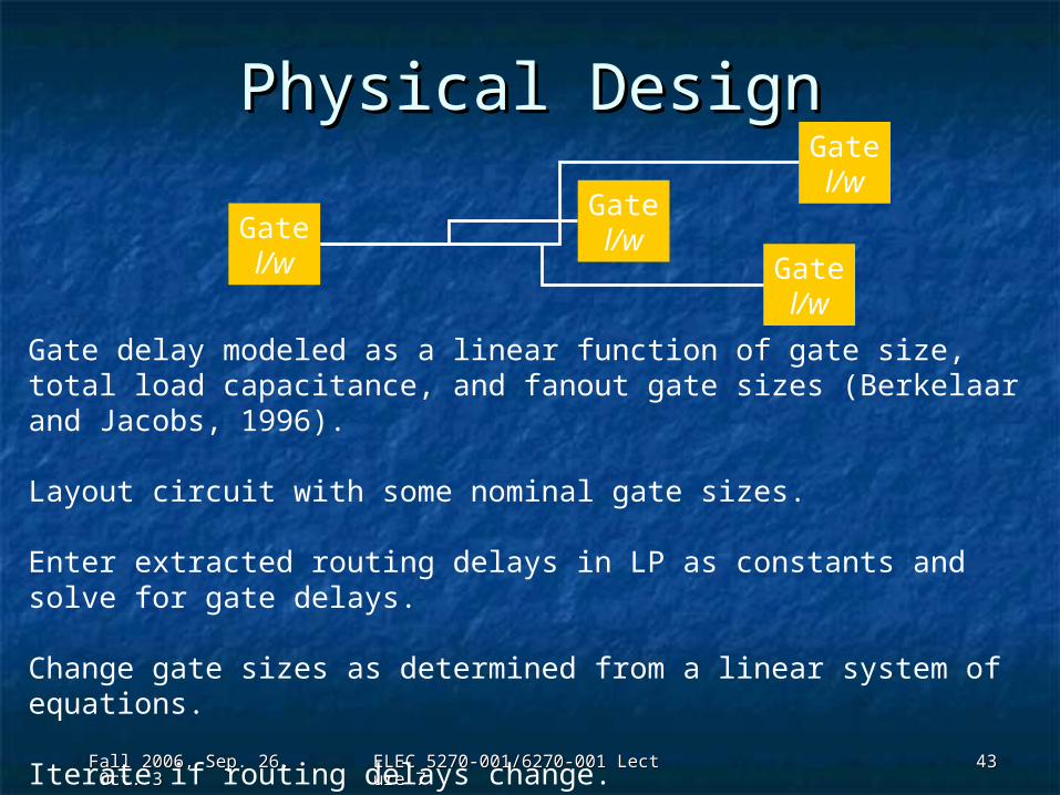
Physical DesignPhysical Design
Gatel/w Gate
l/w
Gatel/w
Gatel/w
Gate delay modeled as a linear function of gate size, total load capacitance, and fanout gate sizes (Berkelaar and Jacobs, 1996).
Layout circuit with some nominal gate sizes.
Enter extracted routing delays in LP as constants and solve for gate delays.
Change gate sizes as determined from a linear system of equations.
Iterate if routing delays change.
Fall 2006, Sep. 26, Oct. 3Fall 2006, Sep. 26, Oct. 3 ELEC 5270-001/6270-001 Lecture 7ELEC 5270-001/6270-001 Lecture 7 4444
Power Dissipation of Power Dissipation of ALU4ALU4
Fall 2006, Sep. 26, Oct. 3Fall 2006, Sep. 26, Oct. 3 ELEC 5270-001/6270-001 Lecture 7ELEC 5270-001/6270-001 Lecture 7 4545
ReferencesReferences R. Fourer, D. M. Gay and B. W. Kernighan, R. Fourer, D. M. Gay and B. W. Kernighan, AMPL: A Modeling AMPL: A Modeling
Language for Mathematical ProgrammingLanguage for Mathematical Programming, South San Francisco: The , South San Francisco: The Scientific Press, 1993.Scientific Press, 1993.
M. Berkelaar and E. Jacobs, “Using Gate Sizing to Reduce Glitch M. Berkelaar and E. Jacobs, “Using Gate Sizing to Reduce Glitch Power,” Power,” Proc. ProRISC WorkshopProc. ProRISC Workshop, Mierlo, The Netherlands, Nov. , Mierlo, The Netherlands, Nov. 1996, pp. 183-188.1996, pp. 183-188.
V. D. Agrawal, “Low Power Design by Hazard Filtering,” V. D. Agrawal, “Low Power Design by Hazard Filtering,” Proc. 10Proc. 10thth Int’l Conf. VLSI DesignInt’l Conf. VLSI Design, Jan. 1997, pp. 193-197., Jan. 1997, pp. 193-197.
V. D. Agrawal, M. L. Bushnell, G. Parthasarathy and R. Ramadoss, V. D. Agrawal, M. L. Bushnell, G. Parthasarathy and R. Ramadoss, “Digital Circuit Design for Minimum Transient Energy and Linear “Digital Circuit Design for Minimum Transient Energy and Linear Programming Method,” Programming Method,” Proc. 12Proc. 12thth Int’l Conf. VLSI Design Int’l Conf. VLSI Design, Jan. 1999, , Jan. 1999, pp. 434-439.pp. 434-439.
M. Hsiao, E. M. Rudnick and J. H. Patel, “Effects of Delay Model in M. Hsiao, E. M. Rudnick and J. H. Patel, “Effects of Delay Model in Peak Power Estimation of VLSI Circuits,” Proc. ICCAD, Nov. 1997, pp. Peak Power Estimation of VLSI Circuits,” Proc. ICCAD, Nov. 1997, pp. 45-51.45-51.
T. Raja, T. Raja, A Reduced Constraint Set Linear Program for Low Power A Reduced Constraint Set Linear Program for Low Power Design of Digital CircuitsDesign of Digital Circuits, Master’s Thesis, Rutgers Univ., New , Master’s Thesis, Rutgers Univ., New Jersey, 2002.Jersey, 2002.

Fall 2006, Sep. 26, Oct. 3Fall 2006, Sep. 26, Oct. 3 ELEC 5270-001/6270-001 Lecture 7ELEC 5270-001/6270-001 Lecture 7 4646
ConclusionConclusion Glitch-free design through LP: constraint-set is linear in the size of Glitch-free design through LP: constraint-set is linear in the size of
the circuit.the circuit.
LP solution:LP solution:
Eliminates glitches at all gate outputs,Eliminates glitches at all gate outputs,
Holds I/O delay within specification, andHolds I/O delay within specification, and
Combines path-balancing and hazard-filtering to minimize the Combines path-balancing and hazard-filtering to minimize the
number of delay buffers.number of delay buffers.
Linear constraint set LP produces results exactly identical to the LP Linear constraint set LP produces results exactly identical to the LP
requiring exponential constraint-set.requiring exponential constraint-set.
Results show peak power savings up to 68% and average power Results show peak power savings up to 68% and average power
savings up to 64%.savings up to 64%.