EE 5340 Semiconductor Device Theory Lecture 12 – Spring 2011
29
EE 5340 Semiconductor Device Theory Lecture 12 – Spring 2011 Professor Ronald L. Carter [email protected] http://www.uta.edu/ronc
-
Upload
aaron-davenport -
Category
Documents
-
view
25 -
download
0
description
EE 5340 Semiconductor Device Theory Lecture 12 – Spring 2011. Professor Ronald L. Carter [email protected] http://www.uta.edu/ronc. Depletion Approximation. - PowerPoint PPT Presentation
Transcript of EE 5340 Semiconductor Device Theory Lecture 12 – Spring 2011
EE 5340Semiconductor Device TheoryLecture 12 – Spring 2011
Professor Ronald L. [email protected]
http://www.uta.edu/ronc
©rlc L12-01Mar2011
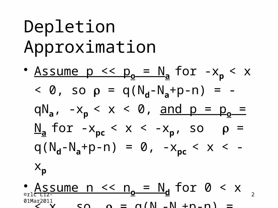
DepletionApproximation• Assume p << po = Na for -xp < x <
0, so r = q(Nd-Na+p-n) = -qNa, -xp
< x < 0, and p = po = Na for -xpc <
x < -xp, so r = q(Nd-Na+p-n) =
0, -xpc < x < -xp
• Assume n << no = Nd for 0 < x <
xn, so r = q(Nd-Na+p-n) = qNd, 0 <
x < xn, and n = no = Nd for xn < x
< xnc, so r = q(Nd-Na+p-n) =
0, xn < x < xnc
2
©rlc L12-01Mar2011
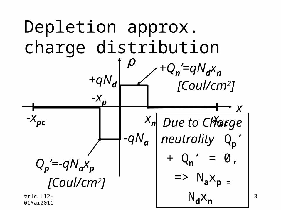
Depletion approx.charge distribution
xn
x-xp
-xpc xnc
r+qNd
-qNa
+Qn’=qNdxn
Qp’=-qNaxp
Due to Charge
neutrality Qp’ + Qn’ =
0, => Naxp =
Ndxn
[Coul/cm2]
[Coul/cm2]3
©rlc L12-01Mar2011
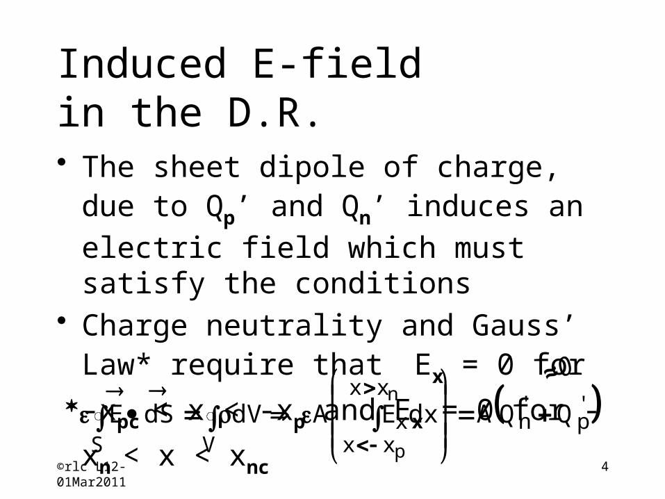
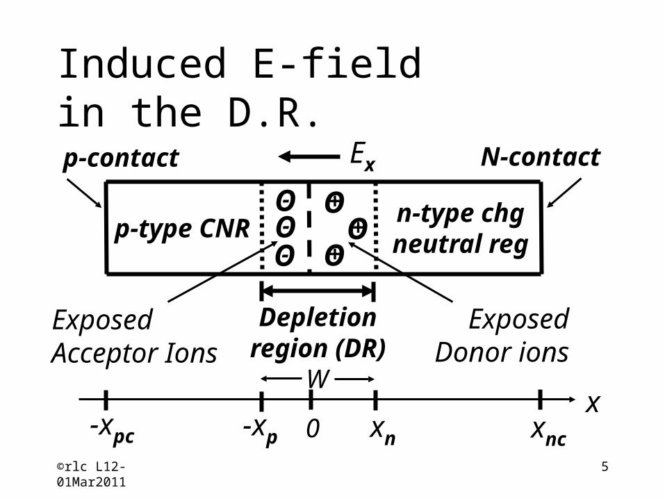
Induced E-fieldin the D.R.• The sheet dipole of charge, due to
Qp’ and Qn’ induces an electric field which must satisfy the conditions
• Charge neutrality and Gauss’ Law* require that Ex = 0 for -xpc < x < -
xp and Ex = 0 for -xn < x < xnc QQAdxEAdVdSE 'p
'n
xx
xxx
VS
n
p
≈0
4
©rlc L12-01Mar2011
Induced E-fieldin the D.R.
xn
x-xp-xpc xnc
O-O-O-
O+O+
O+
Depletion region (DR)
p-type CNR
Ex
Exposed Donor ions
Exposed Acceptor Ions
n-type chg neutral reg
p-contact N-contact
W
05
©rlc L12-01Mar2011
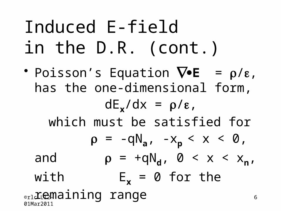
Induced E-fieldin the D.R. (cont.)• Poisson’s Equation E = r/e, has
the one-dimensional form, dEx/dx = r/e,
which must be satisfied for r = -qNa, -xp < x < 0, and r =
+qNd, 0 < x < xn, with
Ex = 0 for the remaining range
6
©rlc L12-01Mar2011
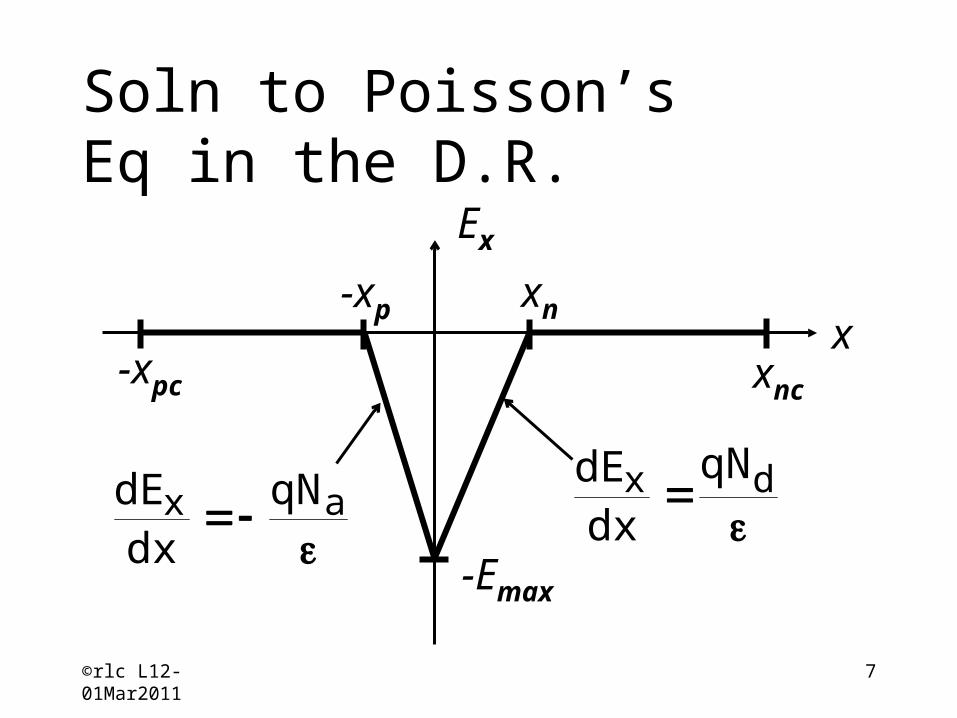
Soln to Poisson’sEq in the D.R.
xnx
-xp
-xpc xnc
Ex
-Emax
dx qN
dxdE
ax qN
dxdE
7
©rlc L12-01Mar2011
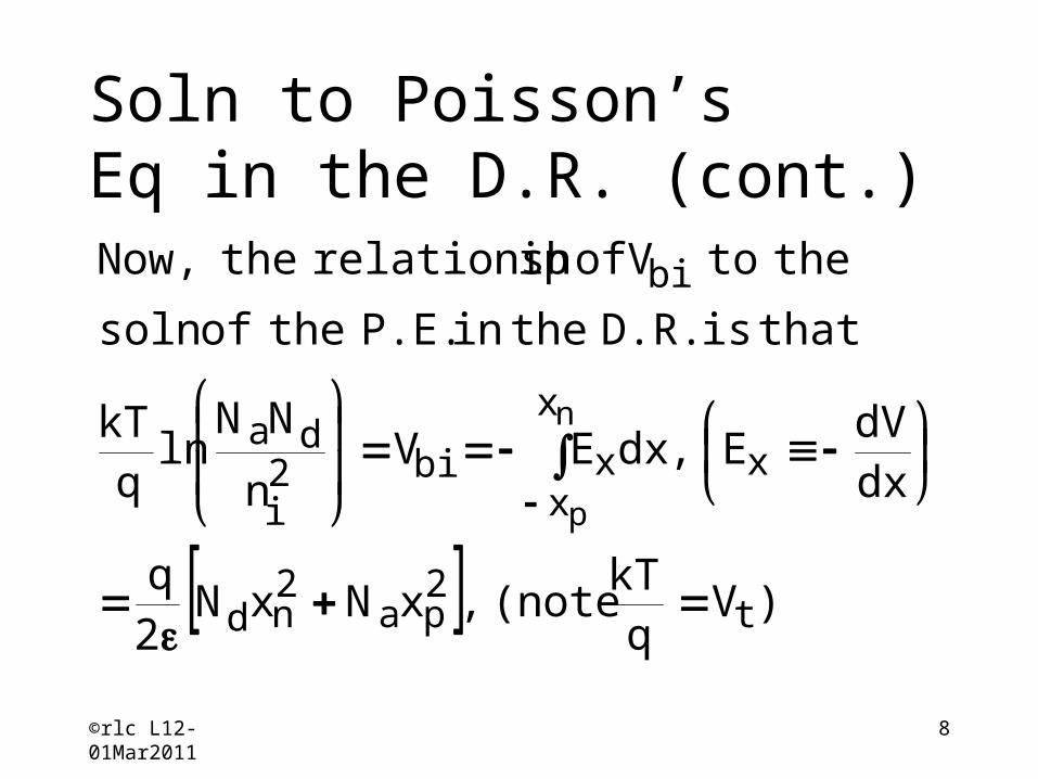
Soln to Poisson’sEq in the D.R. (cont.)
)Vq
kT (note ,xNxN
2q
dxdV
E ,dxEVn
NNln
qkT
that is D.R. the in P.E. the of soln
the to V of iprelationsh the Now,
t2pa
2nd
x
x
xxbi2
i
da
bi
n
p
8
©rlc L12-01Mar2011
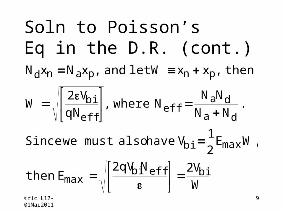
Soln to Poisson’sEq in the D.R. (cont.)
WV2N2qV
E then
,WE21
V have also must we Since
.NN
NNN where ,
qNV2
W
then ,xxW let and ,xNxN
bieffbimax
maxbi
da
daeff
eff
bi
pnpand
9
©rlc L12-01Mar2011
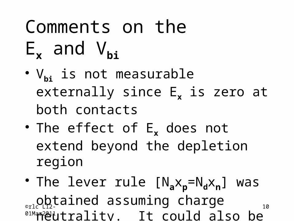
Comments on theEx and Vbi
• Vbi is not measurable externally since Ex is zero at both contacts
• The effect of Ex does not extend beyond the depletion region
• The lever rule [Naxp=Ndxn] was obtained assuming charge neutrality. It could also be obtained by requiring Ex(x=0-dx) = Ex(x=0+dx) = Emax
10
©rlc L12-01Mar2011
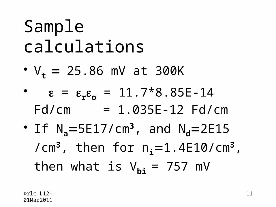
Sample calculations• Vt = 25.86 mV at 300K
• e = ereo = 11.7*8.85E-14 Fd/cm= 1.035E-12 Fd/cm
• If Na=5E17/cm3, and Nd=2E15
/cm3, then for ni=1.4E10/cm3, then
what is Vbi = 757 mV
11
©rlc L12-01Mar2011
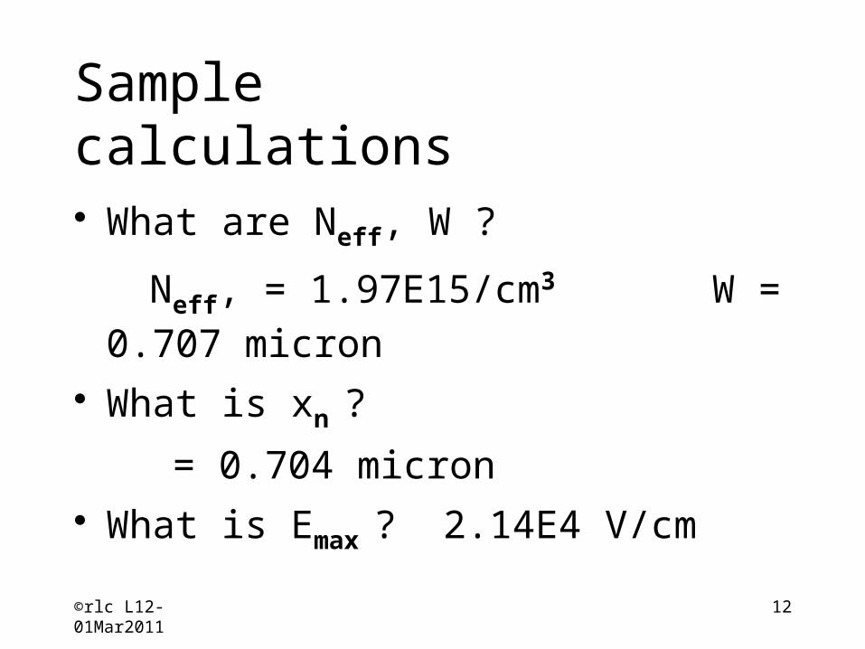
Sample calculations• What are Neff, W ?
Neff, = 1.97E15/cm3
W = 0.707 micron• What is xn ?
= 0.704 micron• What is Emax ? 2.14E4 V/cm
12
©rlc L12-01Mar2011
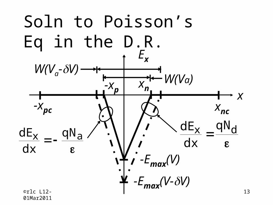
Soln to Poisson’sEq in the D.R.
xnx
-xp
-xpc xnc
Ex
-Emax(V)
dx qN
dxdE
ax qN
dxdE
-Emax(V-dV)
W(Va)W(Va-dV)
13
©rlc L12-01Mar2011
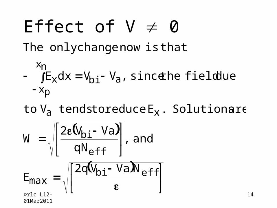
effbimax
eff
bi
xa
abinx
pxx
NVaV2qE
and ,qN
VaV2W
are Solutions .E reduce to tends V to
due field the since ,VVdxE
that is now change only The
Effect of V 0
14
©rlc L12-01Mar2011
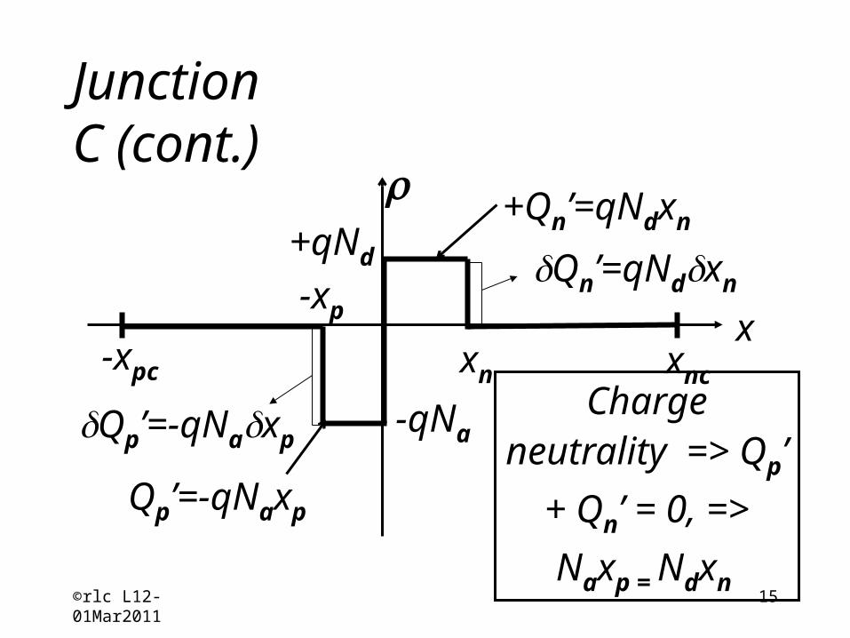
JunctionC (cont.)
xn
x-xp
-xpc xnc
r+qNd
-qNa
+Qn’=qNdxn
Qp’=-qNaxp
Charge neutrality => Qp’ + Qn’ = 0,
=> Naxp = Ndxn
dQn’=qNddxn
dQp’=-qNadxp
15
©rlc L12-01Mar2011
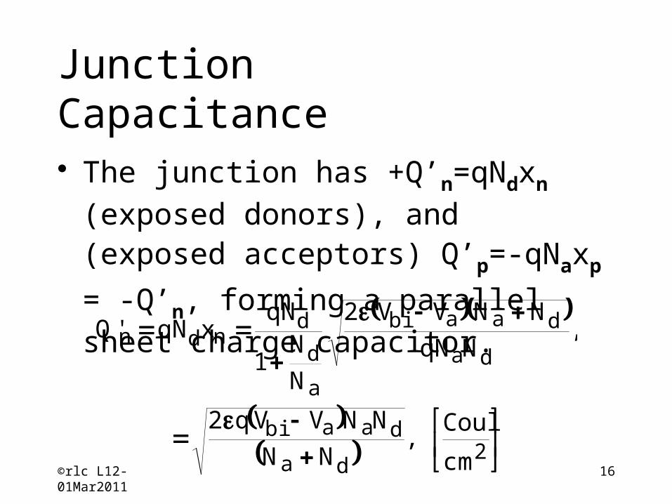
JunctionCapacitance• The junction has +Q’n=qNdxn
(exposed donors), and (exposed acceptors) Q’p=-qNaxp = -Q’n, forming a parallel sheet charge capacitor.
2da
daabi
da
daabi
a
d
dndn
cm
Coul ,
NN
NNVVq2
,NqN
NNVV2
N
N1
qNxqN'Q
16
©rlc L12-01Mar2011
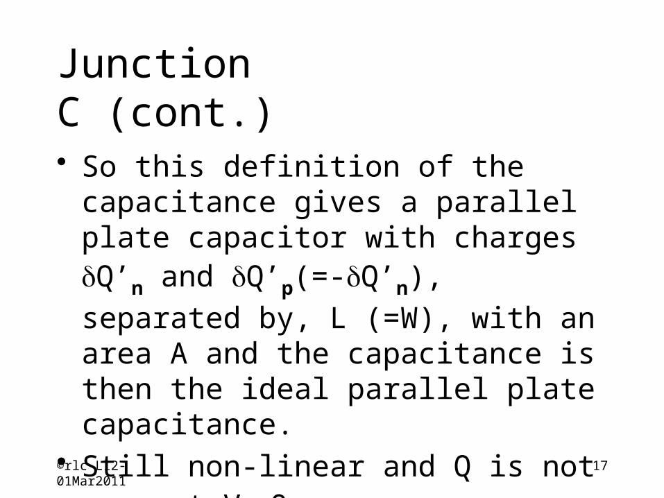
JunctionC (cont.)• So this definition of the
capacitance gives a parallel plate capacitor with charges dQ’n and
dQ’p(=-dQ’n), separated by, L (=W), with an area A and the capacitance is then the ideal parallel plate capacitance.
• Still non-linear and Q is not zero at Va=0.
17
©rlc L12-01Mar2011
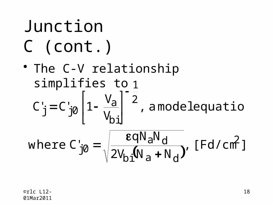
JunctionC (cont.)• The C-V relationship simplifies to
][Fd/cm ,NNV2
NqN'C herew
equation model a ,VV
1'C'C
2
dabi
da0j
21
bi
a0jj
18
©rlc L12-01Mar2011
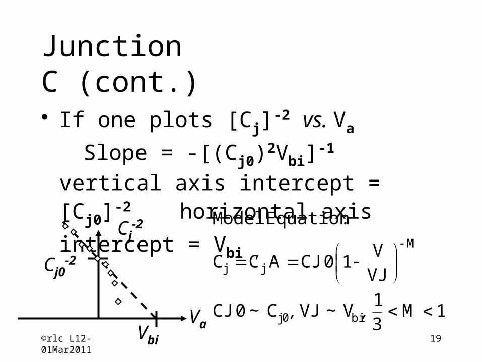
JunctionC (cont.)• If one plots [Cj]
-2 vs. Va
Slope = -[(Cj0)2Vbi]-1
vertical axis intercept = [Cj0]-2 horizontal axis
intercept = Vbi
Cj-2
Vbi
Va
Cj0-2
1M31
VVJ C0CJ
VJV
10CJACC
:Equation Model
bi0j
M
jj
,~,~
'
19
©rlc L12-01Mar2011
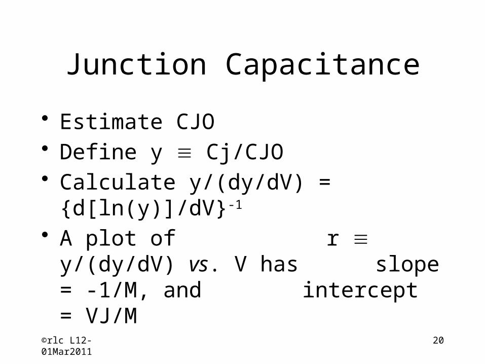
Junction Capacitance
• Estimate CJO• Define y Cj/CJO• Calculate y/(dy/dV) =
{d[ln(y)]/dV}-1
• A plot of r y/(dy/dV) vs. V has
slope = -1/M, andintercept = VJ/M
20
©rlc L12-01Mar2011
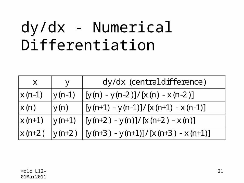
dy/dx - Numerical Differentiation
x y dy/ dx (central diff erence)
x(n-1) y(n-1) [y(n) - y(n-2)]/ [x(n) - x(n-2)]
x(n) y(n) [y(n+1) - y(n-1)]/ [x(n+1) - x(n-1)]
x(n+1) y(n+1) [y(n+2) - y(n)]/ [x(n+2) - x(n)]
x(n+2) y(n+2) [y(n+3) - y(n+1)]/ [x(n+3) - x(n+1)]
21
©rlc L12-01Mar2011
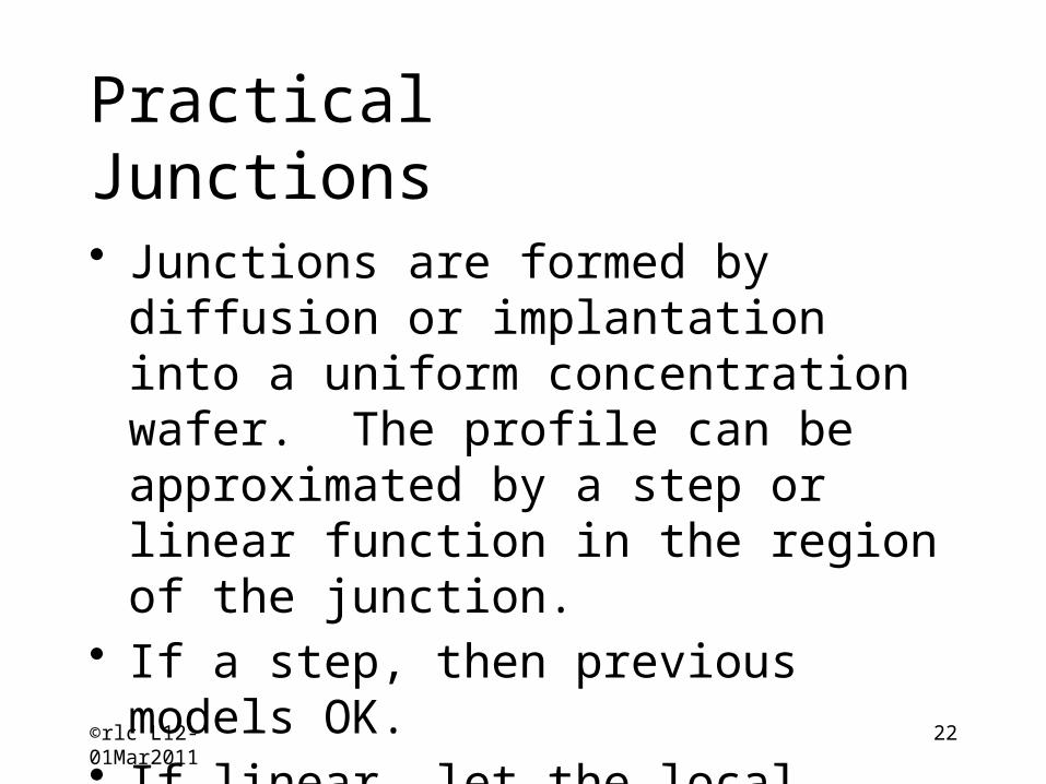
Practical Junctions• Junctions are formed by diffusion
or implantation into a uniform concentration wafer. The profile can be approximated by a step or linear function in the region of the junction.
• If a step, then previous models OK.• If linear, let the local charge
density r=qax in the region of the junction.
22
©rlc L12-01Mar2011
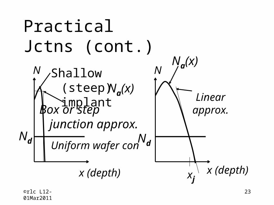
Practical Jctns (cont.)
Shallow (steep) implant
N
x (depth)
Box or step junction approx.
N
x (depth)
Na(x)
xj
Linear approx.
NdNd
Na(x)
Uniform wafer con
23
©rlc L12-01Mar2011
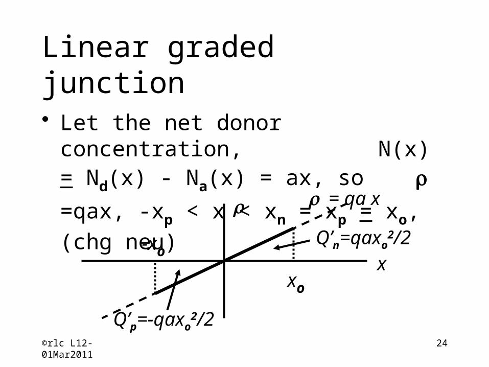
Linear gradedjunction• Let the net donor concentration,
N(x) = Nd(x) - Na(x) = ax, so
r =qax, -xp < x < xn = xp
= xo, (chg neu)
xo
-xo
r r = qa x
Q’n=qaxo2/2
Q’p=-qaxo2/2
x
24
©rlc L12-01Mar2011
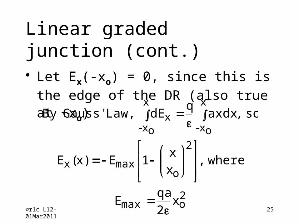
Linear gradedjunction (cont.)• Let Ex(-xo) = 0, since this is the
edge of the DR (also true at +xo)
2omax
2
omaxx
x
ox-
x
ox-x
x2qa
E
where ,xx
1E)x(E
so ,axdxq
dE Law, Gauss' By
25
©rlc L12-01Mar2011
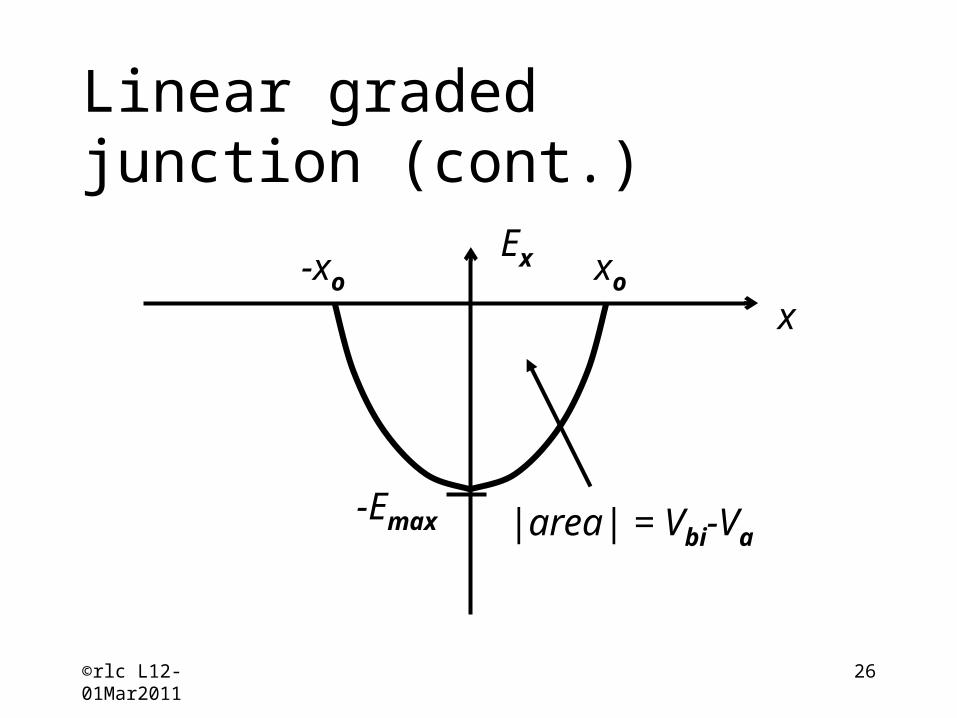
Linear gradedjunction (cont.)
x
Ex
-Emax
xo-xo
|area| = Vbi-Va
26
©rlc L12-01Mar2011
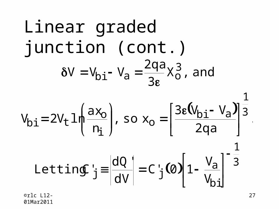
Linear gradedjunction (cont.)
31
bi
ajj
31
abio
i
otbi
3oabi
VV
10C'dV
'dQC' Letting
.qa2
VV3x so ,
nax
lnV2V
and ,X3qa2
VVV
27
©rlc L12-01Mar2011
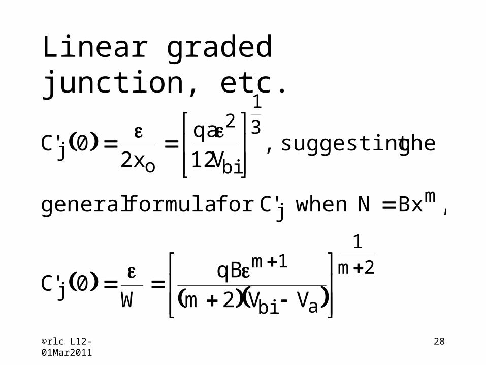
Linear gradedjunction, etc.
2m1
abi
1m
j
mj
31
bi
2
oj
VV2mqB
W0'C
,BxN when 'C for formula general
the suggesting ,V12
qax2
0'C
28
©rlc L12-01Mar2011
29
References1 and M&KDevice Electronics for Integrated
Circuits, 2 ed., by Muller and Kamins, Wiley, New York, 1986. See Semiconductor Device Fundamentals, by Pierret, Addison-Wesley, 1996, for another treatment of the m model.
2Physics of Semiconductor Devices, by S. M. Sze, Wiley, New York, 1981.
3 and **Semiconductor Physics & Devices, 2nd ed., by Neamen, Irwin, Chicago, 1997.
Fundamentals of Semiconductor Theory and Device Physics, by Shyh Wang, Prentice Hall, 1989.