EE 5340 Semiconductor Device Theory Lecture 03 – Spring 2011
description
EE 5340Semiconductor Device TheoryLecture 28 - Fall 2009
Professor Ronald L. [email protected]
http://www.uta.edu/ronc
L 28 Dec 1 2
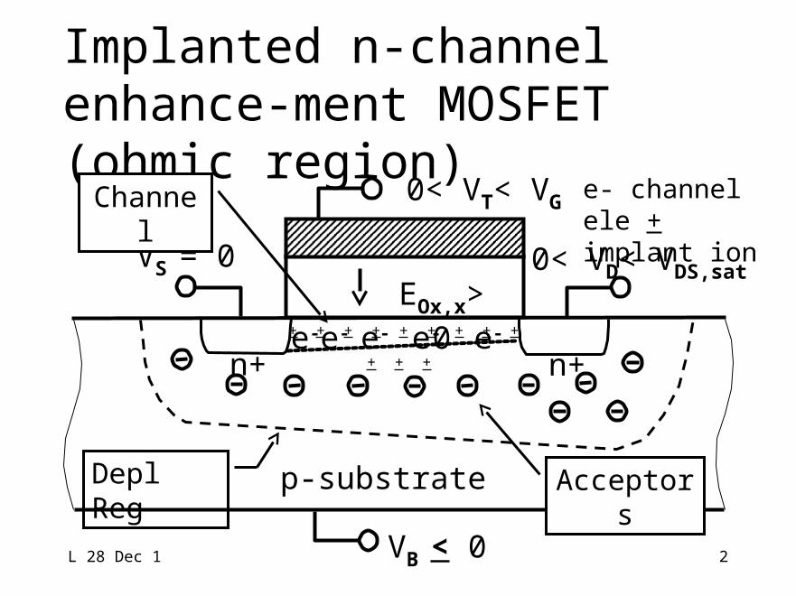
e-e- e- e- e- + + + + + + + + + +
+ +
Implanted n-channel enhance-ment MOSFET (ohmic region)
0< VT< VG
VB < 0
EOx,x> 0
Acceptors
Depl Reg
VS = 0 0< VD<
VDS,sat n+
n+
p-substrate
Channel
e- channel ele + implant ion
L 28 Dec 1 3
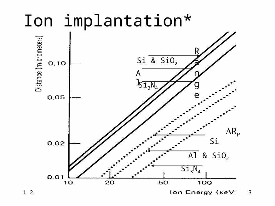
Si & SiO2
AlSi3N4
Si
Al & SiO2
Si3N4
Range
RP
Ion implantation*
L 28 Dec 1 4
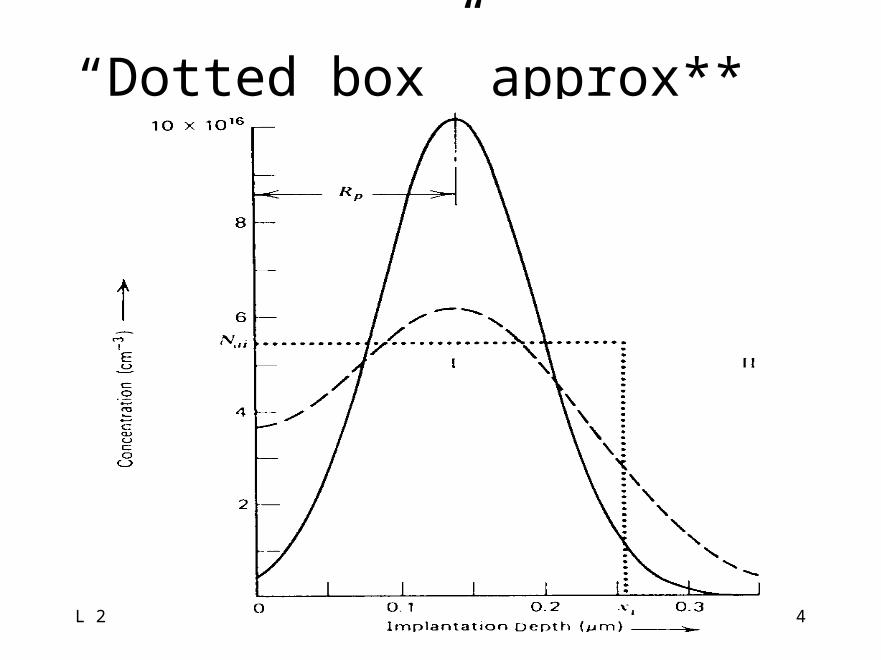
“Dotted box” approx**
L 28 Dec 1 5
curve dottedunder area curve dashedunder area
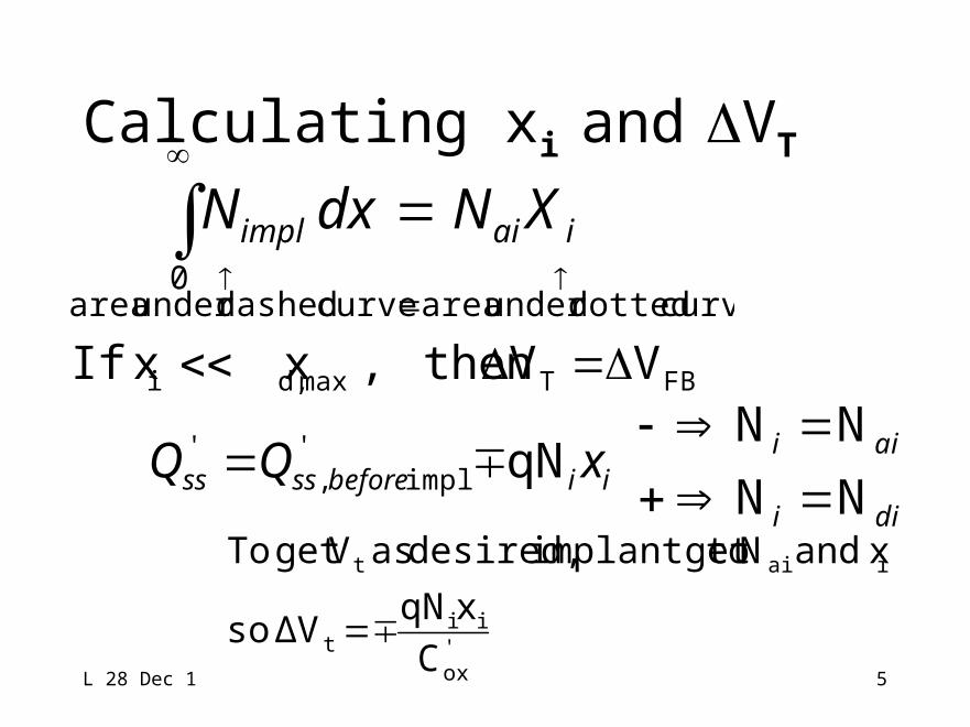
iaiimpl XNdxN 0
'ox
iit
iait
C
xqNΔV so
xand Nget implant to desired, as Vget To
FBTmaxd,i V V then , x xIf
dii
aiiiibeforessss xQQ
NN
NN qN '
impl ,'
Calculating xi and VT

L 28 Dec 1 6
aiaiSBppsa
iai
msxdaiaid
a
aiips
ad
NNxqVqN
xqN
xqNxqNQ
N
Nx
qNx
22
,
2
2
2
If xi ~ xd,max
L 28 Dec 1 7
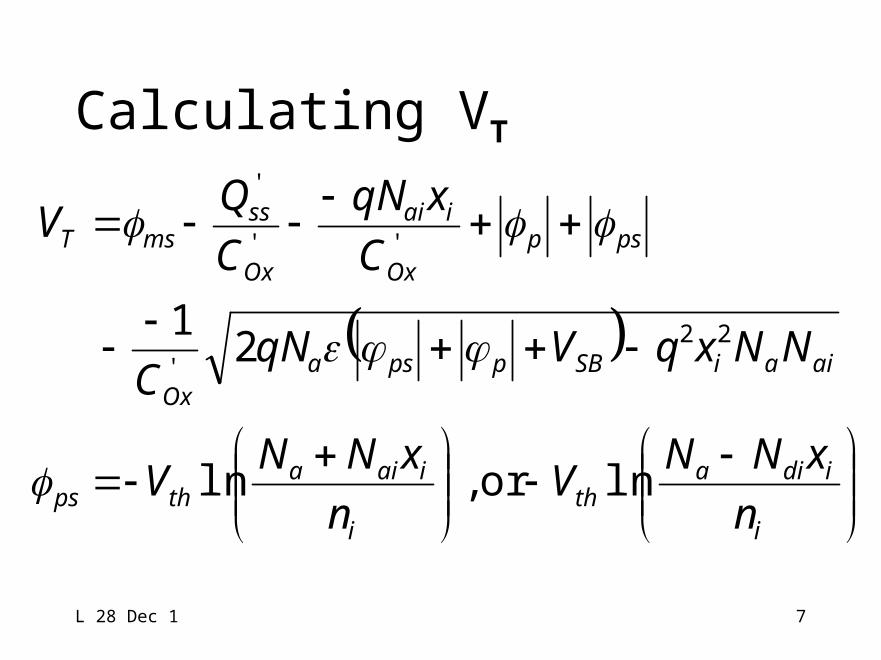
i
idiath
i
iaiathps
aiaiSBppsaOx
pspOx
iai
Ox
ssmsT
n
xNNV
n
xNNV
NNxqVqNC
C
xqN
C
QV
lnor , ln
21 22'
''
'
Calculating VT
L 28 Dec 1 8
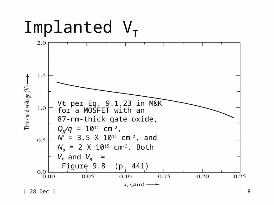
Implanted VT
Vt per Eq. 9.1.23 in M&K for a MOSFET with an 87-nm-thick gate oxide, Qff/q = 1011 cm-2, N’ = 3.5 X 1011 cm-2, and Na = 2 X 1015 cm-3. Both VS and VB = Figure 9.8 (p. 441)
L 28 Dec 1 9
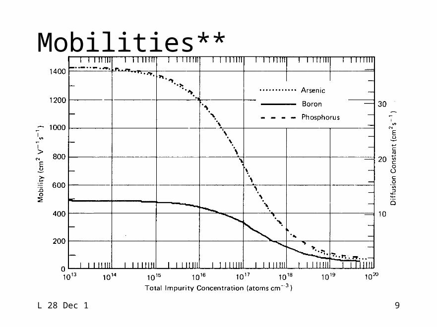
Mobilities**
L 28 Dec 1 10
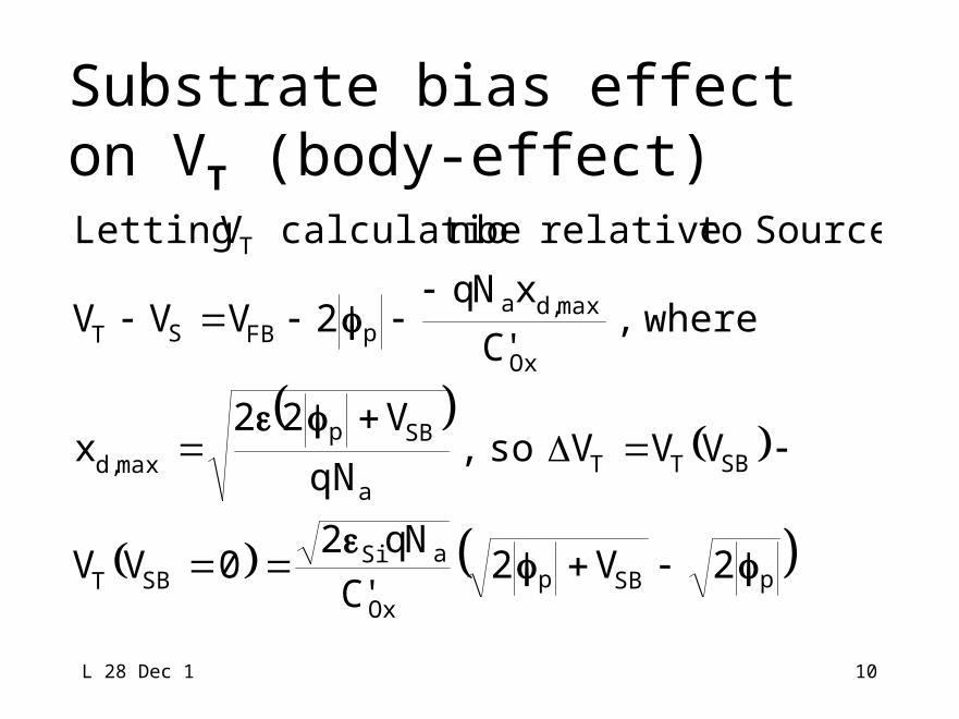
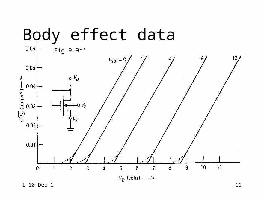
Substrate bias effect on VT (body-effect)
pSBpOx
aSiSBT
SBTTa
SBpmaxd,
Ox
maxd,apFBST
T
2V2'C
Nq20VV
VVV so , qN
V22x
where , 'C
xNq2VVV
Source to relative be ncalculatio V Letting
L 28 Dec 1
Body effect dataFig 9.9**
11
L 28 Dec 1 12
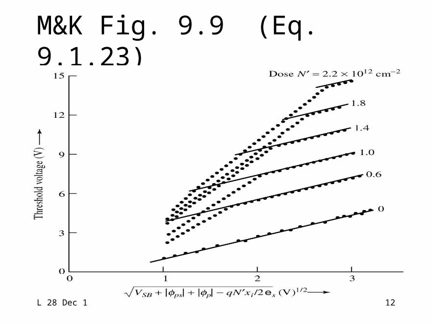
M&K Fig. 9.9 (Eq. 9.1.23)
L 28 Dec 1 13
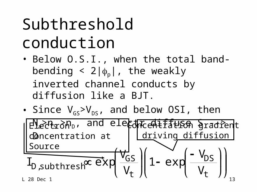
Subthreshold conduction• Below O.S.I., when the total band-
bending < 2|p|, the weakly inverted channel conducts by diffusion like a BJT.
• Since VGS>VDS, and below OSI, then Na>nS
>nD, and electr diffuse S --> D
t
DS
t
GSsubthresh,D V
Vexp1
VV
expI
Electron concentration at Source
Concentration gradient driving diffusion
L 28 Dec 1 14
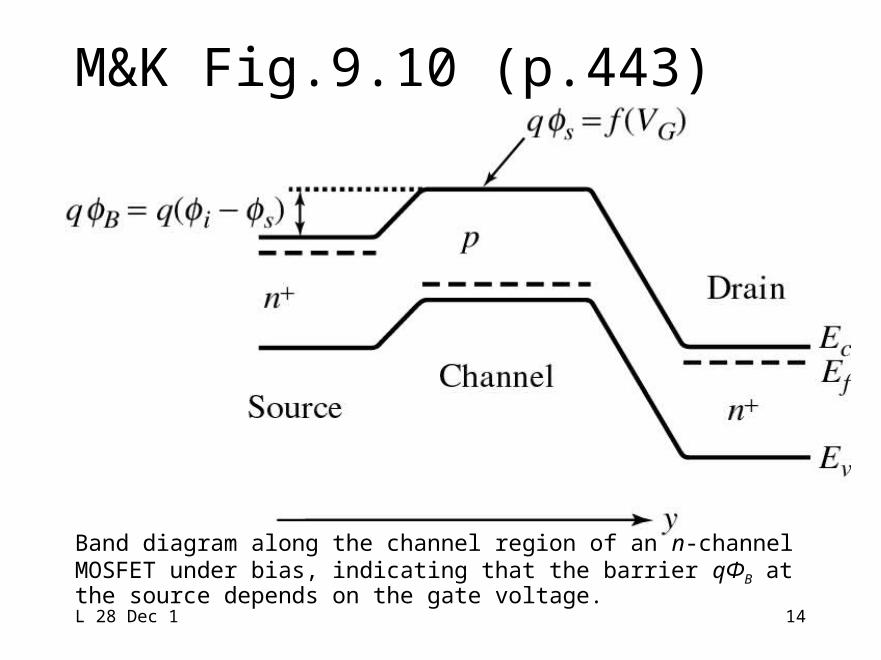
M&K Fig.9.10 (p.443)
Band diagram along the channel region of an n-channel MOSFET under bias, indicating that the barrier qΦB at the source depends on the gate voltage.
L 28 Dec 1 15
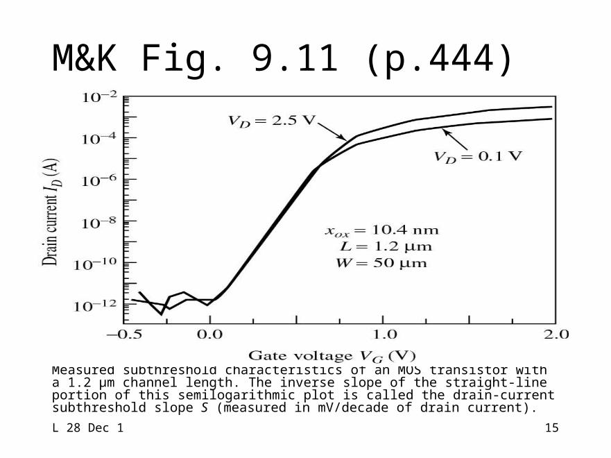
M&K Fig. 9.11 (p.444)
Measured subthreshold characteristics of an MOS transistor with a 1.2 μm channel length. The inverse slope of the straight-line portion of this semilogarithmic plot is called the drain-current subthreshold slope S (measured in mV/decade of drain current).
L 28 Dec 1 16
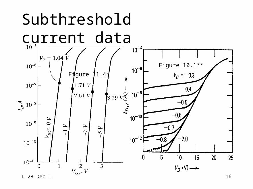
Subthreshold current data
Figure 11.4*
Figure 10.1**
L 28 Dec 1 17
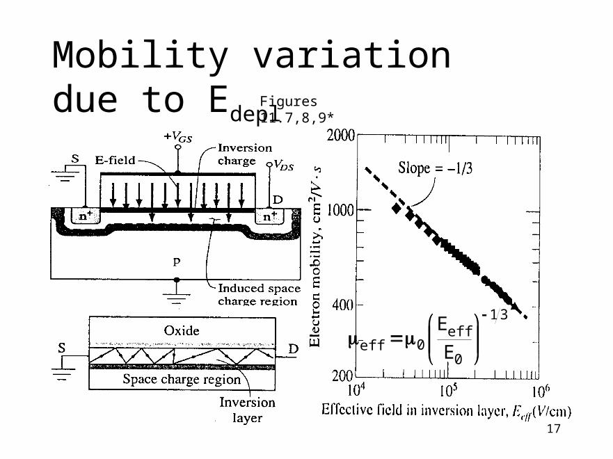
Mobility variationdue to Edepl
Figures 11.7,8,9*
31
0
eff0eff E
E
L 28 Dec 1 18
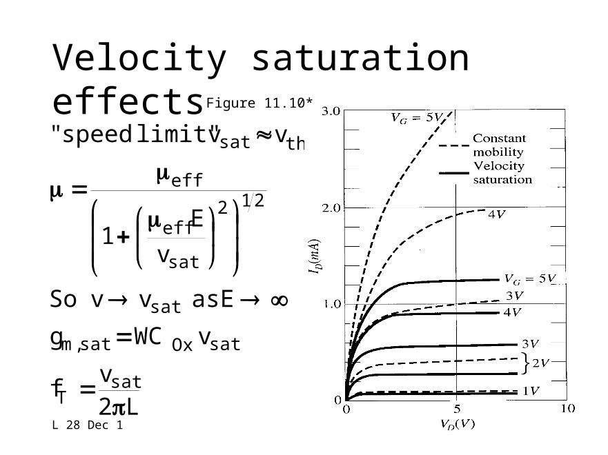
Velocity saturationeffects
L2v
f
vWCg
E as vv So
v
E1
vv limit" speed"
satT
satOxsat,m
sat
212
sat
eff
eff
thsat
Figure 11.10*
L 28 Dec 1 19
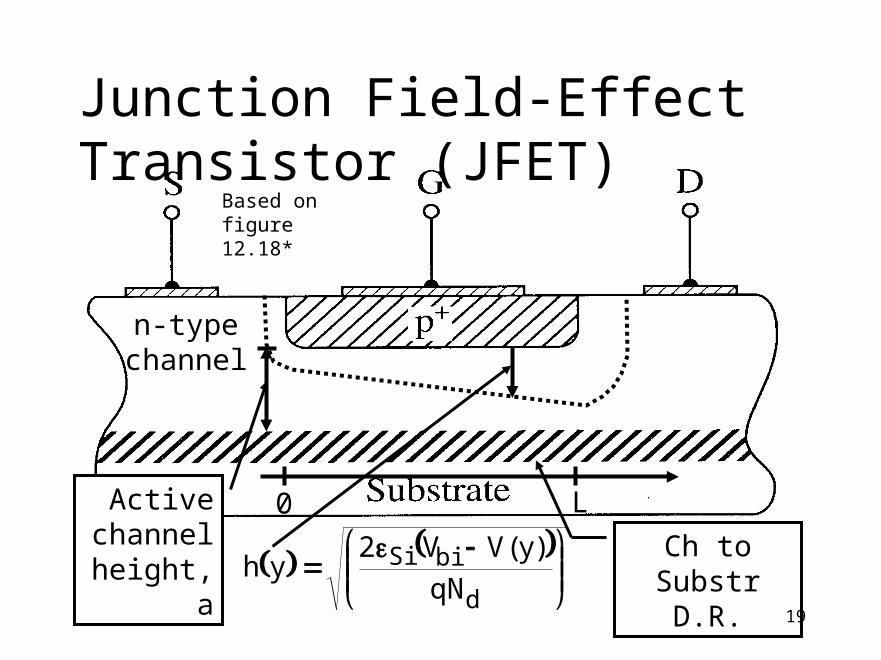
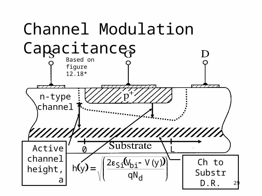
Based on figure 12.18*
n-type channel
L0
Junction Field-Effect Transistor (JFET)
Active channel
height, a
d
biSiqN
)y(VV2yh
Ch to Substr D.R.

L 28 Dec 1 20
Pinch-offVoltage
dCh
aChbipT
bipi
GChtbi
Si
dp
TGS
eff
GSbiSi
NNif
NNifVVV
VV
enhmt
n
NNVV
aqNV
VVaSh
qNVV
Sh
,
if ,ln ,
2
opens channel the then , when ,
ch. n ,NNN
ch. p ,NNN ,
2
2
2
dCheff
aCheff
Note: In depl mode devices, Vp0 > Vbi
L 28 Dec 1 21
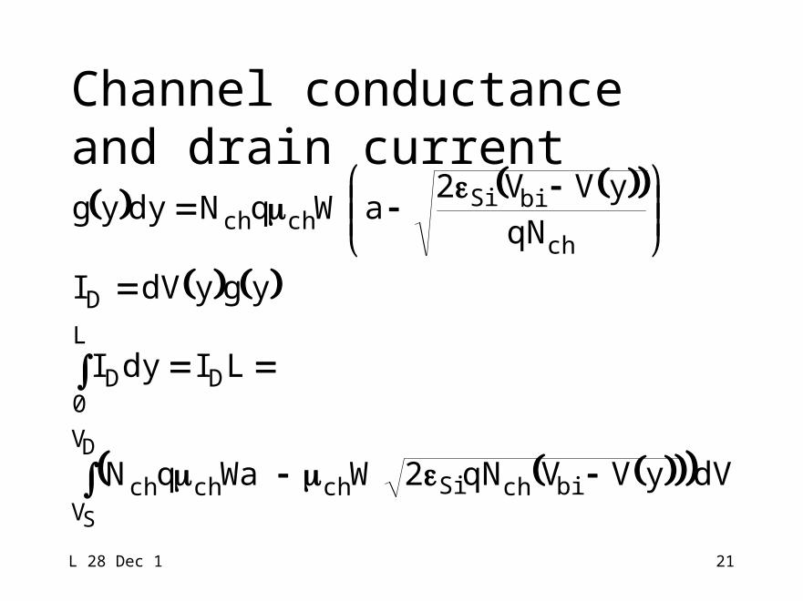
Channel conductanceand drain current
D
S
V
VbichSichchch
D
L
0D
D
ch
biSichch
dVyVVqN2WWaqN
LIdyI
ygydVI
qNyVV2
aWqNdyyg
L 28 Dec 1 22
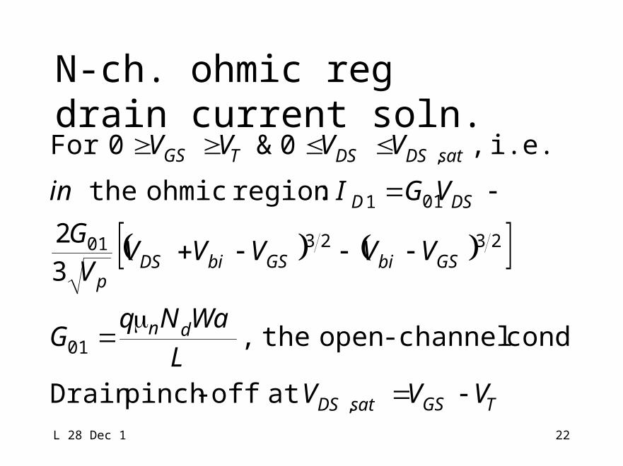
N-ch. ohmic regdrain current soln.
TGSsatDS
dn
GSbiGSbiDSp
DSD
satDSDSTGS
VVVL
WaNqG
VVVVVV
G
VGIin
VVVV
,
01
232301
011
,
at off-pinch Drain
cond. channel-open the ,
32
:region ohmic the
i.e. ,0&0 For
L 28 Dec 1 23
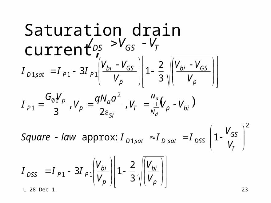
Saturation draincurrent,
p
bi
p
biPPDSS
T
GSDSSsatDsatD
bip
N
NTSi
ap
pP
p
GSbi
p
GSbiPPsatD
VV
VV
III
VV
IIIlawSquare
VVVaqN
VVG
I
VVV
VVV
III
a
d
32
13
1 :approx
, 2
,3
32
13
11
2
,,1
201
1
11,1
TGSDS VVV
L 28 Dec 1 24
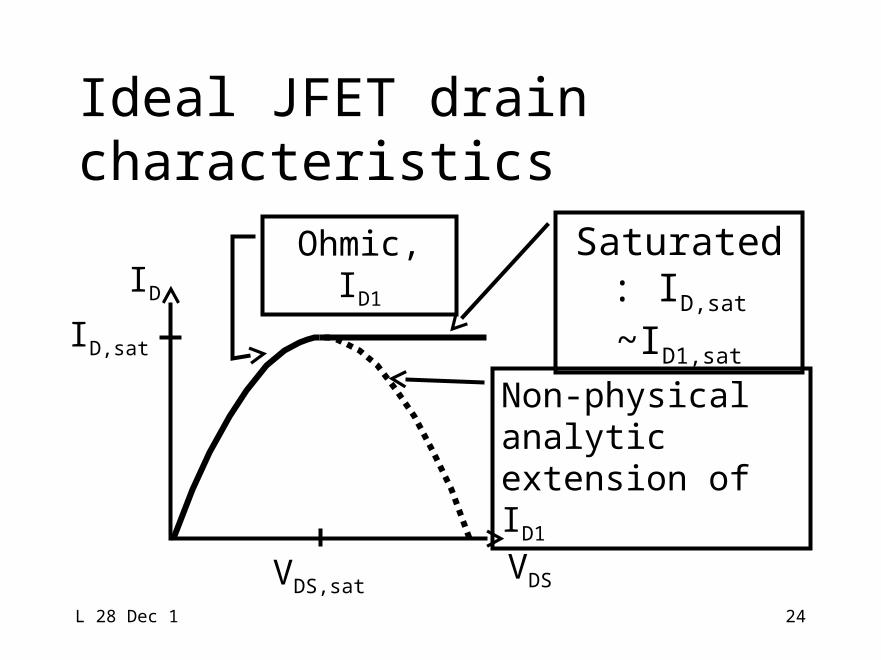
Ideal JFET draincharacteristics
ID
VDSVDS,sat
ID,sat
Ohmic, ID1
Non-physical analytic extension of ID1
Saturated: ID,sat ~ID1,sat
L 28 Dec 1 25
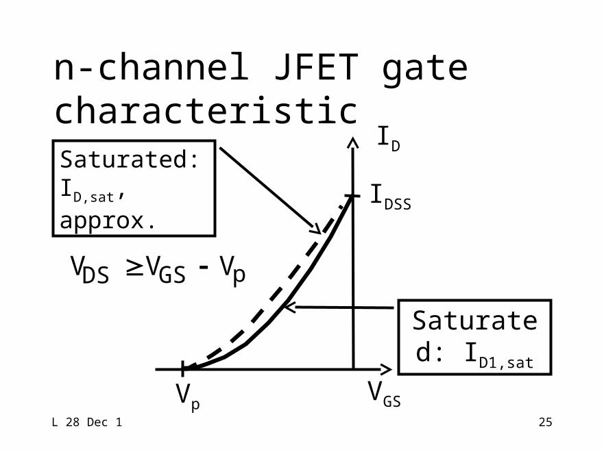
n-channel JFET gatecharacteristic
ID
VGSVp
IDSS
Saturated: ID,sat, approx.
Saturated: ID1,sat
pGSDS VVV
L 28 Dec 1 26
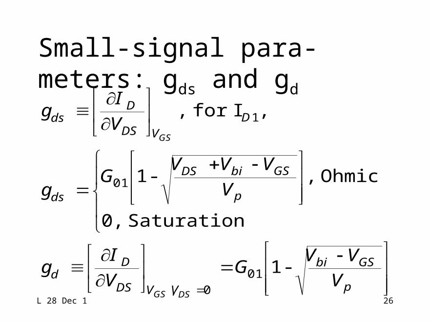
Small-signal para-meters: gds and gd
p
GSbi
VVDS
Dd
p
GSbiDS
ds
DVDS
Dds
VVV
GVI
g
VVVV
Gg
VI
g
DSGS
GS
-1
Saturation ,0
Ohmic ,-1
,I for ,
010,
01
1
L 28 Dec 1 27
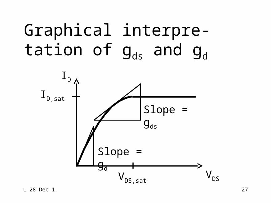
Graphical interpre-tation of gds and gd
ID
VDSVDS,sat
ID,sat
Slope = gds
Slope = gd
L 28 Dec 1 28
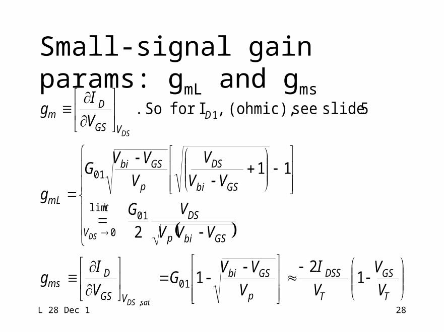
Small-signal gainparams: gmL and gms
T
GS
T
DSS
p
GSbi
VGS
Dms
GSbip
DSit
V
GSbi
DS
p
GSbi
mL
DVGS
Dm
VV
VI
VVV
GVI
g
VVVVG
VVV
VVV
G
g
VI
g
satDS
DS
DS
12
-1
2
11
5 slide see (ohmic), ,I for So .
01
01lim
0
01
1
,
L 28 Dec 1 29
Based on figure 12.18*
n-type channel
L0
Channel ModulationCapacitances
Active channel
height, a
d
biSiqN
)y(VV2yh
Ch to Substr D.R.

L 28 Dec 1 30
Application of JFET theory to MESFET• The channel material is often GaAs• The substrate is often semi-insulating
gallium arsenide (SI GaAs)
• Vbi is replaced by Vnbi, the band-bending
in the semiconductor– Often limited by surface state pinning and
not determined exactly by s
• Neff is now exactly Nch
L 28 Dec 1 31
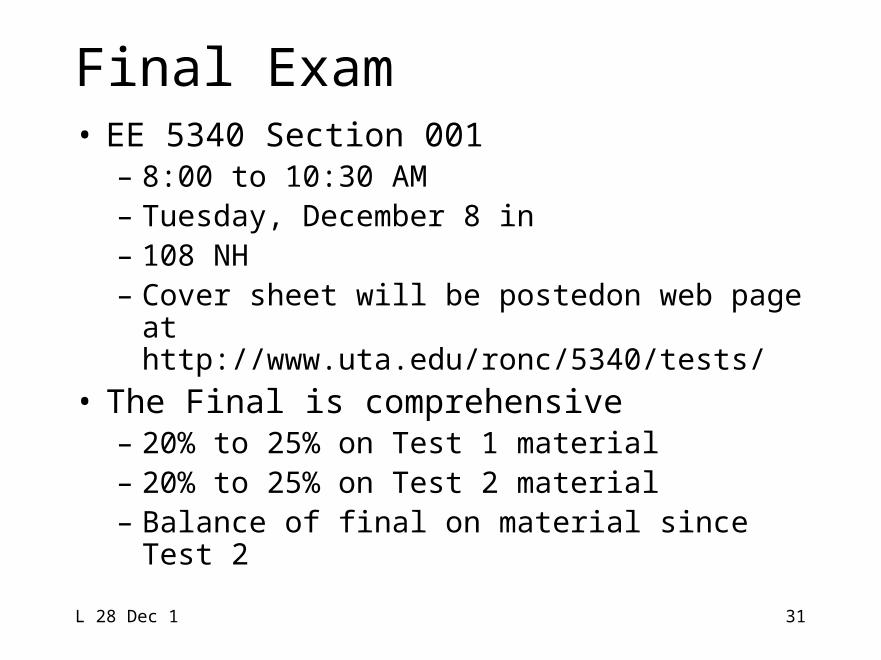
Final Exam• EE 5340 Section 001
– 8:00 to 10:30 AM– Tuesday, December 8 in – 108 NH– Cover sheet will be postedon web page
at http://www.uta.edu/ronc/5340/tests/• The Final is comprehensive
– 20% to 25% on Test 1 material– 20% to 25% on Test 2 material– Balance of final on material since Test
2
L 28 Dec 1
References
* Semiconductor Physics & Devices, by Donald A. Neamen, Irwin, Chicago, 1997.
**Device Electronics for Integrated Circuits, 2nd ed., by Richard S. Muller and Theodore I. Kamins, John Wiley and Sons, New York, 1986
32