TCAD setup for an advanced SiGe HBT technology applied to the HS, MV and HV transistor ... · ·...
23
TCAD setup for an advanced SiGe HBT technology applied to the HS, MV and HV transistor versions 1 STMicroelectronics, 38920 Crolles, France 2 CEDIC, Technische Universität Dresden, 01062 Dresden, Germany 3 IMS, Université Bordeaux I, 33405 Talence, France T. Rosenbaum 1,2,3 , D. Céli 1 , M. Schröter 2 , C. Maneux 3 Bipolar ArbeitsKreis München, Germany, November 25, 2016
Transcript of TCAD setup for an advanced SiGe HBT technology applied to the HS, MV and HV transistor ... · ·...

TCAD setup for an advanced SiGe
HBT technology applied to the HS,
MV and HV transistor versions
1STMicroelectronics, 38920 Crolles, France2CEDIC, Technische Universität Dresden, 01062 Dresden, Germany3IMS, Université Bordeaux I, 33405 Talence, France
T. Rosenbaum1,2,3, D. Céli1, M. Schröter2, C. Maneux3
Bipolar ArbeitsKreis
München, Germany, November 25, 2016
Outline
• Introduction
• TCAD calibration
• Prediction strategy
• Conclusion
2
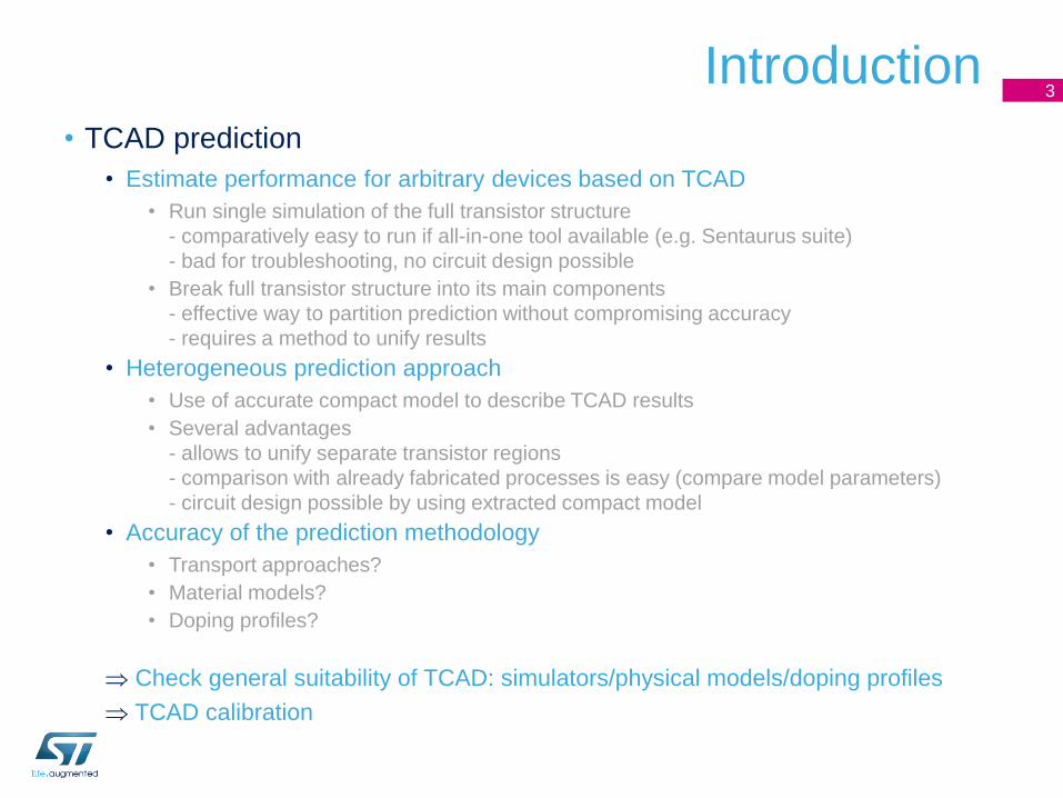
Introduction
• TCAD prediction
• Estimate performance for arbitrary devices based on TCAD
• Run single simulation of the full transistor structure
- comparatively easy to run if all-in-one tool available (e.g. Sentaurus suite)
- bad for troubleshooting, no circuit design possible
• Break full transistor structure into its main components
- effective way to partition prediction without compromising accuracy
- requires a method to unify results
• Heterogeneous prediction approach
• Use of accurate compact model to describe TCAD results
• Several advantages
- allows to unify separate transistor regions
- comparison with already fabricated processes is easy (compare model parameters)
- circuit design possible by using extracted compact model
• Accuracy of the prediction methodology
• Transport approaches?
• Material models?
• Doping profiles?
Check general suitability of TCAD: simulators/physical models/doping profiles
TCAD calibration
3

1D TCAD calibration
4
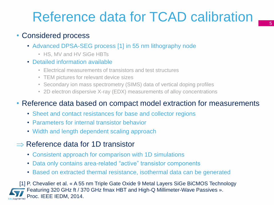
Reference data for TCAD calibration
• Considered process
• Advanced DPSA-SEG process [1] in 55 nm lithography node
• HS, MV and HV SiGe HBTs
• Detailed information available
• Electrical measurements of transistors and test structures
• TEM pictures for relevant device sizes
• Secondary ion mass spectrometry (SIMS) data of vertical doping profiles
• 2D electron dispersive X-ray (EDX) measurements of alloy concentrations
• Reference data based on compact model extraction for measurements
• Sheet and contact resistances for base and collector regions
• Parameters for internal transistor behavior
• Width and length dependent scaling approach
Reference data for 1D transistor
• Consistent approach for comparison with 1D simulations
• Data only contains area-related “active” transistor components
• Based on extracted thermal resistance, isothermal data can be generated
[1] P. Chevalier et al. « A 55 nm Triple Gate Oxide 9 Metal Layers SiGe BiCMOS Technology
Featuring 320 GHz ft / 370 GHz fmax HBT and High-Q Millimeter-Wave Passives ».
Proc. IEEE IEDM, 2014.
5

Reference data for TCAD calibration
• Scalable compact model examples
• Very good agreement for different device widths
• Examples for all three transistor flavors
• VBC = 0 V, fixed emitter length of 9 µm
• 1D data generation is simple
• Set external resistances and capacitances to zero
• Only use area component of internal transistor
(transit time, IT, IB, junction capacitances)
• Generate 1D modelcard for a transistor with AE0 = 1 µm2
Generate reference data by circuit simulation
6
MV HS
HS
HV

Initial 1D TCAD comparison
• Initial PTCAD based results (MV example)
• For physical models
see [2]
• Significant deviation
for transfer current
• Fair agreement for
transit frequency
How to improve agreement?
• Process TCAD simulation, SIMS, EDX and electrical msmt
• Combined approach for accurate profile description
• PTCAD: Delivers first insight into full doping profile view (2D)
• EDX: Germanium content of SiGe layer (2D)
• SIMS: Can be reliably used to detect buried layer doping,
but emitter, base and internal collector region are hard to capture
• Electrical measurement: Allow (partial) reconstruction of doping profile [2]
- in this case to be used for tuning the internal collector doping
[2] T. Rosenbaum et al., « Calibration of 1D doping profiles of SiGe HBTs »,
in Bipolar/BiCMOS Circuits and Technology Meeting - BCTM, 2015 IEEE, Oct 2015, pp. 64-67.
7
VBC = 0 V
MV
MV
Model and profile adjustments
• First step focuses on improving accuracy for transfer current
• Cause for discrepancy?
• Band gap of the base extracted for transfer current (T-dependence): 1.01 eV
• Average band gap of base within simulations: 0.93 eV
• Models impacting band gap of the base
• Band gap narrowing
• Band gap change caused by alloying
Immediate cause cannot be identified
Adjust models by applying identical relative change to both effects
• Adjusting the internal collector doping profile
• Area-related base collector capacitance is known from measurements
• Space charge region (SCR) extension is dominated by collector doping
Tune doping of SCR to match measured capacitance
• Other adjustments
• Model parameters for impact ionization
• Based on all three transistor flavors for unified parameter set
• Auger recombination parameters for base current (unified parameter set)
Redo comparison
8

Comparison for MV transistors
• 1D transistor characteristics
• Very good agreement between measurement based
1D model and hydrodynamic simulations
• Strong link between internal BC capacitance
and ft fall-off observed in simulations
• Discrepancy for transfer current reduced
• Remaining difference at high currents relates
to various factors: extraction accuracy/consistency,
transit time charge, physical models, transport
How about other transistor flavors?
9
MV
VBC = 0 V
MV
MV
MV
Zoom on relevant
region

HS and HV transistor results
• Selected 1D transistor characteristics
• All flavors use identical emitter, SiGe and base profile
• Only a change to the collector doping is applied
• As realized in the fabrication of the devices
• Good agreement with measured FoMs
• Remaining discrepancies
• Only hydrodynamic transport considered here
• Uncertainty on physical models, extraction
and deembedding (for BE capacitance) [appendix]
10
HS
HS
HV HV
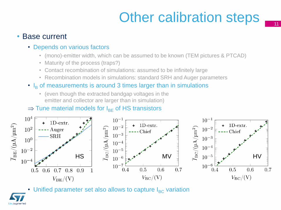
Other calibration steps
• Base current
• Depends on various factors
• (mono)-emitter width, which can be assumed to be known (TEM pictures & PTCAD)
• Maturity of the process (traps?)
• Contact recombination of simulations: assumed to be infinitely large
• Recombination models in simulations: standard SRH and Auger parameters
• IB of measurements is around 3 times larger than in simulations
• (even though the extracted bandgap voltages in the
emitter and collector are larger than in simulation)
Tune material models for IBE of HS transistors
• Unified parameter set also allows to capture IBC variation
11
HS MV HV

Other calibration steps
• Impact ionization
• For small negative VBC, secondary electron hole pairs play a minor role
• Adjust generation rate of electrons for this region (npn transistor)
• At larger bias, generation of holes by II becomes important, see [3]
• For used generation models refer to [4]
• Two step adjustment for the multiplication factor
• Limited VBC range (left) for electrons and full VBC range (right) for electrons and holes
Multiplication
factor Ma vs. bias
Good agreement for all three flavors using a unified parameter set
[3] C. Canali et al., « Experimental and Monte Carlo analysis of impact-ionization in AlGaAs/GaAs
HBTs », IEEE Transaction on Electron Devices, 1996.
[4] T. Rosenbaum et al., « Breakdown mechanisms in advanced SiGe HBTs: scaling and TCAD
calibration », in Bipolar Arbeitskreis, Unterpremstätten, 2015.
12
Prediction approach
13
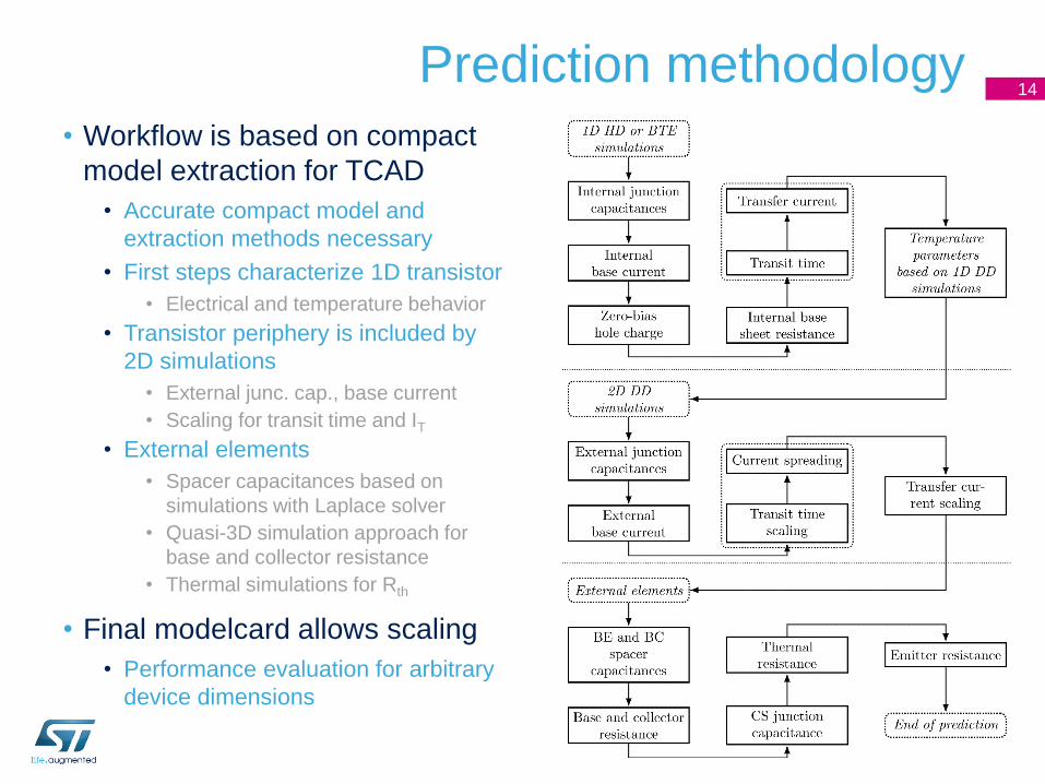
Prediction methodology
• Workflow is based on compact
model extraction for TCAD
• Accurate compact model and
extraction methods necessary
• First steps characterize 1D transistor
• Electrical and temperature behavior
• Transistor periphery is included by
2D simulations
• External junc. cap., base current
• Scaling for transit time and IT
• External elements
• Spacer capacitances based on
simulations with Laplace solver
• Quasi-3D simulation approach for
base and collector resistance
• Thermal simulations for Rth
• Final modelcard allows scaling
• Performance evaluation for arbitrary
device dimensions
14

BE and BC spacer capacitances
• Basic idea
• Laplace equation
• Charge of contact (2D)
• Normal vector of contact
surface is parallel to field
• Capacitance
• Simulation setup
• Laplace equation solver POICAPS [5]
• Implement structure of process into 2D input file
considering relevant regions
• Apply relative permittivity based on material properties
• Example for BC spacer
• Conductive materials (assume identical potential)
• Collector via, sinker and buried layer
• Base via, silicide, polysilicon
• Isolation incorporates relevant materials based on TEM
[5] G. Wedel, POICAPS - A multidimensional numerical capacitance simulator, 2012.
15
𝑑𝑖𝑣 −𝜀𝑔𝑟𝑎𝑑 𝜓 = 0
𝑄′ = ර𝐷 𝑑റ𝑠 = ර𝜀𝐸 𝑑റ𝑠 = ර𝜀𝐸 𝑑𝑠
𝐶′ = 𝑄′/𝑈

Base and collector resistance
• Quasi-3D simulation setup [6]
• 2D simulation region considers conductive layer (either base or buried layer)
• Assign specific sheet resistances to each layer region (single value for BL)
• Current injected into internal regions along the conductive layer
• Current “disappears” from the resistive sheet (either internal collector or monoemitter)
Apply constant (geometry independent) recombination rate over internal region
• Calculation of sheet resistances
• Homogeneously doped layer (e.g. 1017/cm3)
• Different mobility for respective regions
to match sheet resistances
• Base resistance calculation
• Identical principle, but additional
sheet resistance regions
• E.g. BE spacer, polysilicon, silicide regions
[6] M. Schroter and S. Lehmann, « The rectangular bipolar transistor tetrode structure
and its application », in ICMTS ’07, March 2007, pp. 206-209.
16
1
𝑅𝑠= 𝑞න
𝑥𝑠
𝑥𝑒
𝑛𝜇𝑛 + 𝑝𝜇𝑝 𝑑𝑥

Thermal resistance
• Thermal simulation setup
• Heat equation solver THERMO [7]
• Implement structure of process into
3D input file, considering relevant regions
• Apply thermal conductivity based on
material properties
• Place heat source at BC junction
- dimension is set according to space charge
region extension and current spreading
- different size for each of the flavors
• Temperature distribution
• Exemplary device with lE0 ≈ 4.5 µm, bE0 ≈ 100 nm
• DTI isolation confines heatflow
• Largest temperature increase at center of device
• Result for thermal resistance overestimates
extraction result by only 5 – 15 %
• Metallization not included in simulations
[7] G. Wedel, THERMO - A numerical, multi-dimensional heat flow equation solver, 2009.
17
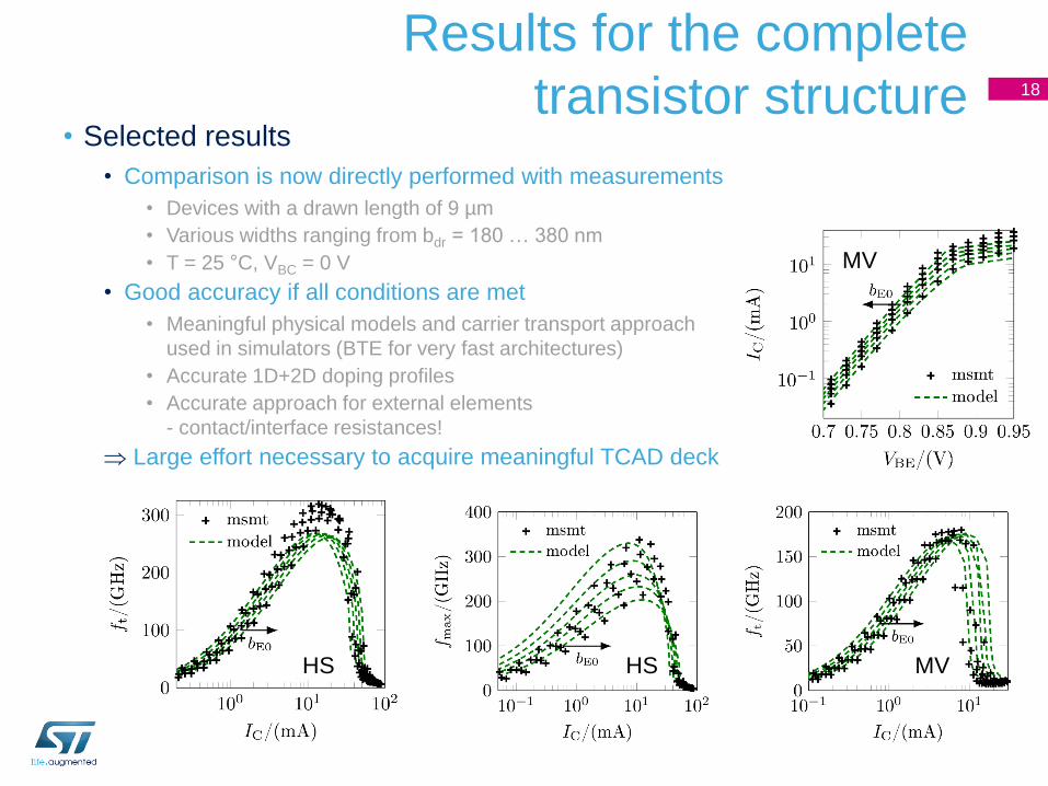
Results for the complete
transistor structure• Selected results
• Comparison is now directly performed with measurements
• Devices with a drawn length of 9 µm
• Various widths ranging from bdr = 180 … 380 nm
• T = 25 °C, VBC = 0 V
• Good accuracy if all conditions are met
• Meaningful physical models and carrier transport approach
used in simulators (BTE for very fast architectures)
• Accurate 1D+2D doping profiles
• Accurate approach for external elements
- contact/interface resistances!
Large effort necessary to acquire meaningful TCAD deck
18
HS HS
MV
MV

2D profile importance
• HV transistors
• Well proximity effect (WPE)
• Played an important role for
HV transistor prototype
• Very low buried layer doping
• Cannot be detected by SIMS
Insufficient information for
profile tuning
• 2D PTCAD profile result
• WPE not taken into account
for process simulations
• Leads to incorrect collector
current spreading
• Internal collector resistance
is too large
• Manual change of collector
spreading angle (rhs figures)
• Improved agreement
19
HV HV
HV HV

Conclusion
• Overview on TCAD calibration
• Based on extraction applied to measurements
• Generation of 1D characteristics (reference)
• Bandgap adjustment
• Improvement for collector current
• Collector doping
• Adjustment for BC junction capacitance and ft fall-off
• Recombination and impact ionization models
• TCAD prediction example for an advanced SiGe HBT technology
• Agreement depends on variety of factors
• Doping profiles, physical models, external elements
• 2D doping profiles can be a bottleneck
• Less impact expected for future architectures with small internal collector width
=> less current spreading
20

References[1] P. Chevalier et al. « A 55 nm Triple Gate Oxide 9 Metal Layers SiGe BiCMOS Technology
Featuring 320 GHz ft / 370 GHz fmax HBT and High-Q Millimeter-Wave Passives ».
Proc. IEEE IEDM, 2014.
[2] T. Rosenbaum et al., « Calibration of 1D doping profiles of SiGe HBTs »,
in Bipolar/BiCMOS Circuits and Technology Meeting - BCTM, 2015 IEEE, Oct 2015, pp. 64-67.
[3] C. Canali et al., « Experimental and Monte Carlo analysis of impact-ionization in AlGaAs/GaAs
HBTs », IEEE Transaction on Electron Devices, 1996.
[4] T. Rosenbaum et al., « Breakdown mechanisms in advanced SiGe HBTs: scaling and TCAD
calibration », in Bipolar Arbeitskreis, Unterpremstätten, 2015.
[5] G. Wedel, POICAPS - A multidimensional numerical capacitance simulator, 2012.
[6] M. Schroter and S. Lehmann, « The rectangular bipolar transistor tetrode structure
and its application», in ICMTS ’07, March 2007, pp. 206-209.
[7] G. Wedel, THERMO - A numerical, multi-dimensional heat flow equation solver, 2009.
21

Thank you for your attention!
22

Backup slides
• Open deembedding
• CSB,o, CSC,o, CSE,o are much larger than all other metallization capacitances
• Geometry independent
Impact on small devices is larger
• Substrate is shorted with emitter in transistor test structures
• Common emitter configuration leads to
23
𝐶𝐵𝐸 = 𝐶𝐵𝐸,𝑡𝑜𝑡 − 𝐶𝐵𝐸,𝑜 − 𝐶𝑆𝐵,𝑜