Future of SiGe HBT Technology and Its Applications
16
7 Future of SiGe HBT Technology and Its Applications M. Schr ¨ oter 1,2 , U. Pfeiffer 3 and R. Jain 3 1 Chair for Electron Devices and Integrated Circuits, Technische Universit¨ at Dresden, Germany 2 Department of Electrical and Computer Engineering, University of California at San Diego, USA 3 Institute for High-Frequency and Communication Technology (IHCT), University of Wuppertal, Germany 7.1 Introduction The results of DOTSEVEN described in the previous chapters of this book mark a milestone in the development of SiGe HBT technology. This chapter reflects on how this milestone fits into the overall picture of semiconductor technologies with potential for high-speed/high-frequency applications. Fur- thermore, as any milestone is a temporary state, the possible future prospects of SiGe HBT device performance will be presented in terms of a roadmap. Finally, obstacles on the path toward the perceived performance limits of this technology are discussed. 7.2 Technology Comparison Circuits operating at mm-wave frequencies have traditionally been imple- mented in III–V semiconductors due to the higher mobility in these materials. However, the high mobility occurs only at relatively low electric fields, which are easily exceeded under circuit-relevant bias conditions, especially when trying to generate high output power. Nevertheless, the fastest HBTs today have been fabricated in InP technology with the respective proto- typing processes reaching (f T , f max ) values around (0.5, 1.1) THz for emitter widths of 130 nm [Urte11] and 200 nm [Bol16]. Compared to these 309
Transcript of Future of SiGe HBT Technology and Its Applications
7Future of SiGe HBT Technology
and Its Applications
M. Schroter1,2, U. Pfeiffer3 and R. Jain3
1Chair for Electron Devices and Integrated Circuits, Technische UniversitatDresden, Germany2Department of Electrical and Computer Engineering, University ofCalifornia at San Diego, USA3Institute for High-Frequency and Communication Technology (IHCT),University of Wuppertal, Germany
7.1 Introduction
The results of DOTSEVEN described in the previous chapters of this bookmark a milestone in the development of SiGe HBT technology. This chapterreflects on how this milestone fits into the overall picture of semiconductortechnologies with potential for high-speed/high-frequency applications. Fur-thermore, as any milestone is a temporary state, the possible future prospectsof SiGe HBT device performance will be presented in terms of a roadmap.Finally, obstacles on the path toward the perceived performance limits of thistechnology are discussed.
7.2 Technology Comparison
Circuits operating at mm-wave frequencies have traditionally been imple-mented in III–V semiconductors due to the higher mobility in these materials.However, the high mobility occurs only at relatively low electric fields,which are easily exceeded under circuit-relevant bias conditions, especiallywhen trying to generate high output power. Nevertheless, the fastest HBTstoday have been fabricated in InP technology with the respective proto-typing processes reaching (fT, fmax) values around (0.5, 1.1) THz foremitter widths of 130 nm [Urte11] and 200 nm [Bol16]. Compared to these
309

310 Future of SiGe HBT Technology and Its Applications
Figure 7.1 Operating speed comparison between SiGeC HBTs, InP HBTs, and MOSFETsvs. critical lithography dimensions (i.e., emitter width or channel length): (a) maximumoscillation frequency and (b) transit frequency. The lines represent LSQ fits of the data, thered filled squares DOTSEVEN results, and the larger crosses the best InP HBT data.
devices, DOTSEVEN SiGe HBTs with (fT, fmax) = (0.5, 0.72) THz areabout one generation behind in terms of power gain cutoff frequencyx.This performance difference is displayed in Figure 7.1, which includes fTand fmax data of the three mainstream technology contenders gathered frommany publications [Ros16]. The DOTSEVEN results have been marked bythe red squares.
Although InP HBTs do have certain advantages over SiGeC HBTs such ashigher breakdown voltage (at the same speed) and the potential of combinedoptical/electronic operation, it was shown in [Voi04] that “at comparable fTand fmax, there is very little difference in their performance in narrow-bandmm-wave and in broadband and high-speed digital circuits”; i.e., for circuitapplications, the advantage of the higher breakdown voltage in InP HBTsappears to be relatively small.
A main disadvantage of III–V technologies is their fairly low integrationlevel and yield as well as the difficulty of structural downscaling due tostrong surface recombination and the resulting low current gain. Hence, itwill be difficult to leverage these technologies to their full extent to enableboth more complex mm-wave systems and, in particular, mass-market wafervolume in the future. As a consequence, III–V material-based technologies donot achieve functionality and energy efficiency increases comparable to thoseof silicon technology, which in turn makes it difficult for them to competealso on cost. In addition, the relatively large process variations and thelack of accurate modeling tools have notoriously hampered (cost-) efficientIII–V circuit design. Therefore, the III–V semiconductor industry and the
7.2 Technology Comparison 311
related investment have been focused strongly on high-frequency/high-speedlow-volume niche applications. The market success of more recentapproaches toward a heterogeneous integration with completed CMOSwafers (e.g., [Ram12]) remains unclear yet. Among the issues are certainlythe very different process qualification criteria in the silicon (especially thedigital CMOS) world and in the III–V world.
According to Figure 7.1 the cutoff frequencies of the best RF-CMOSprocesses come close to those of SiGe HBTs, but at the expense of asignificantly more advanced lithography, typically at least three lithographynodes. Achieving the DOTSEVEN results though would require a CMOSprocess with about a 14 nm channel length (which does not correspond to the14 nm node!), assuming that progress in device speed continues for CMOS assketched by the corresponding dashed line in Figure 7.1. As will be discussedlater below, this assumption is unlikely to be the case.
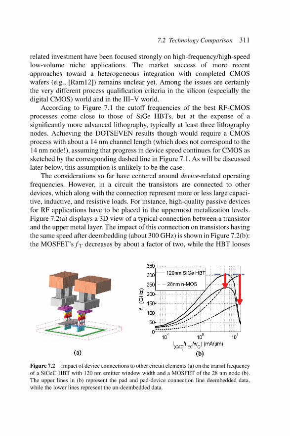
The considerations so far have centered around device-related operatingfrequencies. However, in a circuit the transistors are connected to otherdevices, which along with the connection represent more or less large capaci-tive, inductive, and resistive loads. For instance, high-quality passive devicesfor RF applications have to be placed in the uppermost metalization levels.Figure 7.2(a) displays a 3D view of a typical connection between a transistorand the upper metal layer. The impact of this connection on transistors havingthe same speed after deembedding (about 300 GHz) is shown in Figure 7.2(b):the MOSFET’s fT decreases by about a factor of two, while the HBT looses
Figure 7.2 Impact of device connections to other circuit elements (a) on the transit frequencyof a SiGeC HBT with 120 nm emitter window width and a MOSFET of the 28 nm node (b).The upper lines in (b) represent the pad and pad-device connection line deembedded data,while the lower lines represent the un-deembedded data.

312 Future of SiGe HBT Technology and Its Applications
about 20% of its speed. Similar observations have been noted in [Ina11],where the peak operating frequencies (fT, fmax) of 45 nm MOSFETs dropby a factor of two, once the metallization necessary for building circuits isincluded. The reason why HBTs do not show this severe deterioration istheir much higher transconductance gm and corresponding drive capability.In other words, devices with the same ratio of gm and input capacitance havethe same fT, but devices with a higher gm will fundamentally fare better incircuits since the device capacitance there will only be a more or less smallfraction of the total capacitance.
Based on the observations described above, it is therefore instructive tolook at the values of gm when comparing process technology performance,since gm represents a better indication of achievable circuit speed. Figure 7.3shows the measured and predicted values of gm for a variety of incumbentand emerging process technologies. For comparison, gm has been normalizedto emitter length (for HBTs), gate width (for planar MOSFETs), or channelperimeter length (for nano-wire and -tube FETs1). It is clearly visible thatHBTs have a much higher transconductance per finger length than FETs.Furthermore, FETs appear to be unable to ever catch up to HBTs in terms oftransconductance, even when assuming ideal performance scaling accordingto the approximation of existing data (dashed lines).
Figure 7.3 also includes the transconductance values for future technol-ogy nodes, which have been predicted based on detailed TCAD simulationsand compact models for complete 3D transistors with all relevant parasiticsincluded [Sch17, Voi17] and have become the basis for the 2014 and 2015ITRS tables. For MOSFETs, the peaks of gm (around 4 mS/µm) and fT(around 600 GHz) are predicted for a channel length of 10 nm, while beyondthat length the strong impact of surface scattering in the extremely thinchannel layer will lead to a drastic decrease (to, e.g., gm ≈ 1.5 mS/µm, fT≈ 200 GHz). This is in stark contrast to HBT scaling, which significantlybenefits from smaller dimensions in all aspects of electrical performanceuntil a critical base width is reached and the small emitter area leads to ahigh emitter contact resistance.2 The ultimate performance of SiGe HBTswas investigated in [Sch11a, Sch11b] using detailed TCAD simulation and
1Normalizing to the perimeter takes into account (roughly) that screening effects wouldlead to a lower gm value if the wires or tubes were placed next to each other, which wouldcorrespond to a normalization to the diameter (or minimum footprint for a gate-all-aroundchannel).
2Note though that the impact of contact resistances increases with smaller device dimen-sions in all technologies and becomes visible first in highly scaled FETs.

7.2 Technology Comparison 313
Figure 7.3 Comparison of the terminal (or extrinsic) transconductance of transistors froma large variety of process technologies. Filled symbols represent measured data and opensymbols represent predicted (roadmap) data. For FETs, the legend designations correspond tothe channel material and structure: planar III–V such as InGaAs (III–V bulk); planar single-or few atomic layers such as black phosphorus or germanane (2D); planar transition metaldichalcogenide such as MoS2 (TMD); planar or FinFET silicon (Si-CMOS); nano-wire siliconor III–V (NW); carbon nano-tube (CNT).
accurate compact models with all known physical effects and device-relatedparasitics included. The predictions resulted in a transit frequency between0.8 and 1 THz and maximum oscillation frequency around 2 THz, dependingon the assumed contact resistivities especially for the emitter. For the ITRStables (see also [Sch17] for more details), quite conservative values have beenassumed, which lead to somewhat reduced device operating frequencies andtransconductances compared to [Sch11b].
The doping profile of the technology node N3, the performance of whichwas predicted in 2013, served as the guideline for the DOTSEVEN processdevelopment. During process development, accurate physics-based modelparameters were determined based on which the evaluation of the impactof the various physical and parasitic effects on device performance [Kor15,Paw17] is possible. This strategy provided valuable insight for prioritizingthe process development tasks. It is interesting to note that the electricalparameters, such as base sheet resistance and capacitance per area, of thefinal process version of DOTSEVEN meet those of the roadmap node N3predicted earlier quite well. This validates the accuracy of the predictions andthe employed approach.

314 Future of SiGe HBT Technology and Its Applications
The predicted progress in device speed is closely linked to the increasein current densities required for achieving peak operating frequencies. Thecorresponding transconductance at the device terminals is more or lessstrongly reduced by the emitter series (contact) resistance. With conservativeassumptions about contact resistivities, transconductance values of at least40 mS/µm can be expected according to Figure 7.3 at the present end ofthe roadmap. This value remains an order of magnitude higher than thatpredicted for the best MOSFETs and also still higher than that predictedfor the best CNTFETs by a factor of four. Notice that due to the lack ofsufficient hardware, the predictions of the latter are associated with muchhigher uncertainty than those for MOSFETs.
An important aspect for mm-wave and THz applications is the achievableoutput power at a given frequency. For advanced MOSFET technologies, thelatter is impacted significantly by the decrease of the voltage gain, whichis caused by the increased output leakage and associated output conduc-tance. HBTs do not show this decrease unless they are scaled (vertically)beyond the last node presently shown in the ITRS tables. Output power canalso be increased with device size. While this increases the device-relatedcapacitances in both HBTs and MOSFETs, an increase in emitter lengthalone reduces all series resistances in HBTs but a corresponding gate widthincrease in FETs leads to a larger gate resistance. Moreover, the maximumallowed drain–source voltage in advanced RF-MOSFETs is lower than themaximum collector–emitter voltage in advanced high-speed HBTs. Increas-ing the number of parallel devices in MOSFET-based power amplifiers leadsto larger interconnect parasitics per unit drain width, while stacked poweramplifier architectures require a larger number of devices and thus again morepassives and parasitics per unit drain width. Another important building blockin (sub-)mm-wave systems is the VCO. Its phase noise strongly dependson the flicker (1/f ) noise of the transistors. Here, HBTs have much lowercorner frequencies than MOSFETs, in which 1/f noise keeps increasing formore advanced nodes. Overall, HBTs appear to have a distinctive advantagein the area of mm-wave and THz amplifiers from a technical circuit designperspective.
Finally, a few words on cost. With the development and added masks forthe required RF-passives, an RF-CMOS process becomes significantly morecostly than the corresponding digital process. Thus, a depreciated CMOSprocess with high-speed SiGe HBTs integrated (i.e., a BiCMOS process)can often be cheaper and thus very cost competitive to advanced RF-CMOS.Such a BiCMOS process not only provides better RF front-end performance

7.3 Future Millimeter-wave and THz Applications 315
(in terms of analog HF features and energy efficiency) but is also earlieravailable on the market. In view of these aspects, RF-CMOS based on anadvanced node makes sense only for applications that require (i) higher digitalfunctionality and density than an already available BiCMOS process withcomparable front-end (i.e., HBT) performance and (ii) very high productvolume.
Due to the already existing large investment and associated infrastructurein 200 and 300 mm silicon wafer fabs around the world, SiGe:C HBTs withoperating speed in the THz range are desirable. Implemented into depreciated(and hence low-cost) digital CMOS platforms, the associated SiGe:C BiC-MOS single-chip technologies are capable of covering (at reasonable wafercost) medium- and large-volume applications with mm-wave and THz analogfront-ends, which would be either far too expensive when implemented inmost advanced CMOS technology or would not even be possible to realizethere due to the inferior analog characteristics of future advanced MOS-FETs as discussed above. Therefore, a relatively small investment in SiGe:CHBT process development will yield large gains in terms of (ultimatelycommodity) market coverage.
7.3 Future Millimeter-wave and THz Applications
The terahertz or sub-millimeter frequency range, roughly defined as extend-ing from 300 GHz to 3 THz, has so far resisted attempts to broadly harnessits potential for everyday applications. This led to the expression THz gap,loosely describing the lack of adequate technologies to effectively bridge thistransition region between microwaves and optics – both readily accessible viawell-developed electronic and laser-based approaches – by, e.g., integratedand cost-efficient electronics. THz technology is an emerging field which hasdemonstrated a wide-ranging potential. Extensive research in the last yearshas identified many attractive application areas and paved the technologi-cal path toward broadly usable THz systems. THz technology is currentlyin a pivotal phase and will soon be able to radically expand our analyticcapabilities via its intrinsic benefits.
Applications of mm-wave and THz frequencies led by the silicon inte-grated technologies can be subdivided into communication, radar, imaging,and sensing areas, as illustrated in Figure 7.4. In the following sections, wedescribe some of these applications and the recent, state-of-the-art hardwaredevelopments in the corresponding areas as it relates to DOTSEVEN.

316 Future of SiGe HBT Technology and Its Applications
Figure 7.4 Potential applications for silicon integrated mm-wave and THz circuits.
7.3.1 Communication
To improve the data capacity beyond 10 Gbps for wireless transmission,improving the spectral efficiency with advanced modulation schemes is nolonger sufficient and higher bandwidth becomes an absolutely necessity. Themm-wave and THz bands, due to their large relative bandwidth, show greatpotential for future wireless communication [Son11]. Such large frequen-cies, however, suffer from greater atmospheric attenuation as compared tothe traditional radio waves. Still, the atmospheric windows near 90 GHz,140 GHz, and 240 GHz are being considered for future communication andradar applications [Fed10].
7.3 Future Millimeter-wave and THz Applications 317
Due to a larger atmospheric attenuation, the THz waves are expectedto be first used for indoor wireless personal-area (WPAN) and local-area(WLAN) networks, where the range is limited to a few tens of meters at themost. Along with the high-capacity, the high directivity of THz waves is alsoconsidered as an advantage to ensure secure (requiring line-of-sight) or high-density, non-interfering data networks. Some of the possible applications ofTHz communication are:
1. Wireless distribution of HDTV content in an in-home network. Whilethe current 60 fps, progressive full HD (1080p60) content requires datatransmission rates near 3 Gbps, future ultra HD 8K content wouldrequire wireless data transmission rates in the ballpark of 24 Gbps[Son11].
2. High-bandwidth wireless backhauls in high-density mesh multipoint topoint/multipoint (first-mile and last-mile) networks may require datarates reaching 100 Gbps.
3. Rapid uploading and downloading of large files from a server which canserve as a public data kiosk.
4. Inter- and intra-building communication networks for manufacturingfloor automation, etc.
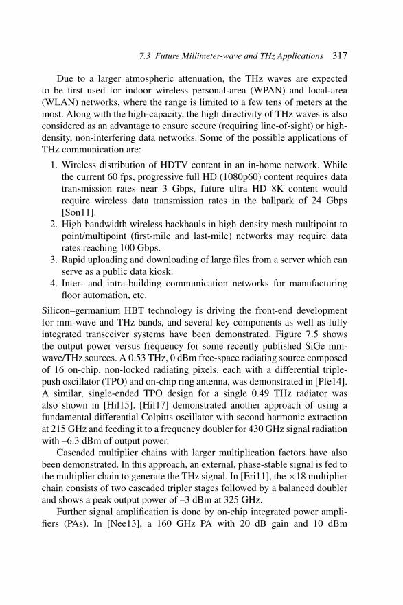
Silicon–germanium HBT technology is driving the front-end developmentfor mm-wave and THz bands, and several key components as well as fullyintegrated transceiver systems have been demonstrated. Figure 7.5 showsthe output power versus frequency for some recently published SiGe mm-wave/THz sources. A 0.53 THz, 0 dBm free-space radiating source composedof 16 on-chip, non-locked radiating pixels, each with a differential triple-push oscillator (TPO) and on-chip ring antenna, was demonstrated in [Pfe14].A similar, single-ended TPO design for a single 0.49 THz radiator wasalso shown in [Hil15]. [Hil17] demonstrated another approach of using afundamental differential Colpitts oscillator with second harmonic extractionat 215 GHz and feeding it to a frequency doubler for 430 GHz signal radiationwith –6.3 dBm of output power.
Cascaded multiplier chains with larger multiplication factors have alsobeen demonstrated. In this approach, an external, phase-stable signal is fed tothe multiplier chain to generate the THz signal. In [Eri11], the ×18 multiplierchain consists of two cascaded tripler stages followed by a balanced doublerand shows a peak output power of –3 dBm at 325 GHz.
Further signal amplification is done by on-chip integrated power ampli-fiers (PAs). In [Nee13], a 160 GHz PA with 20 dB gain and 10 dBm
318 Future of SiGe HBT Technology and Its Applications
Figure 7.5 Frequency versus output power of some recently published SiGe integrated mm-wave/THz sources.
saturated output power (Psat) was demonstrated. A parallel power-combination approach with four PA cores was used in [Nee16] to show 25 dBgain and 9 dBm Psat for 200–225 GHz.
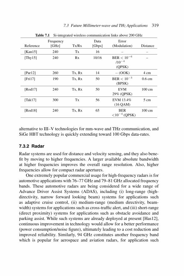
In the recent years, fully integrated silicon RF front-ends operating above200 GHz have become feasible due to the continuous technology improve-ment. Both CMOS [Kan15, Thy15, Par12, Tak17] and SiGe [Fri17, Rod17,Rod18] front-ends have been reported in the literature. Circuits using sub-harmonic techniques with doubler or tripler as last stage before the antennalike a 240 GHz transceiver chipset utilizing QPSK in 65 nm CMOS canbe found in the combination of [Kan15] and [Thy15]. A 260 GHz OOKtransceiver in 65 nm bulk CMOS was reported in [Par12]. [Tak17] presents aCMOS transmitter working at 300 GHz capable of communicating over 5 cmat 56 Gbps. A complete SiGe chipset for 50 Gbps at mm distance is presentedby [Fri17]. In [Rod17], a SiGe integrated 240 GHz transceiver chipset inthe DOTSEVEN technology (as detailed in Chapter 6) is reported with adata-rate of 50 Gbps communicating over 100 cm distance. The data ratewas further improved to 65 Gbps by post-process IF filtering at the receiver-end in [Rod18]. A comparison of these front-ends is presented in Table 7.1.Extensive research in device technology and circuits continues to improve theperformance further, indicating that SiGe HBTs are becoming a formidable
7.3 Future Millimeter-wave and THz Applications 319
Table 7.1 Si-integrated wireless communication links above 200 GHz
ReferenceFrequency
[GHz] Tx/RxData
[Gbps]Error
(Modulation) Distance
[Kan15] 240 Tx 16 – –
[Thy15] 240 Rx 10/16 BER < 10−6
/10−4
(QPSK)
–
[Par12] 260 Tx, Rx 14 − (OOK) 4 cm
[Fri17] 190 Tx, Rx 50 BER < 10−3
(BPSK)0.6 cm
[Rod17] 240 Tx, Rx 50 EVM29% (QPSK)
100 cm
[Tak17] 300 Tx 56 EVM 13.4%(16 QAM)
5 cm
[Rod18] 240 Tx, Rx 65 BER<10−4 (QPSK)
100 cm
alternative to III–V technologies for mm-wave and THz communication, andSiGe HBT technology is quickly extending toward 100 Gbps data-rates.
7.3.2 Radar
Radar systems are used for distance and velocity sensing, and they also bene-fit by moving to higher frequencies. A larger available absolute bandwidthat higher frequencies improves the overall range resolution. Also, higherfrequencies allow for compact radar apertures.
One extremely popular commercial usage for high-frequency radars is forautomotive applications with 76–77 GHz and 79–81 GHz allocated frequencybands. These automotive radars are being considered for a wide range ofAdvance Driver Assist Systems (ADAS), including (i) long-range (high-directivity, narrow forward looking beam) systems for applications suchas adaptive cruise control, (ii) medium-range (medium directivity, beam-width) systems for applications such as cross-traffic alert, and (iii) short-range(direct proximity) systems for applications such as obstacle avoidance andparking assist. While such systems are already deployed at present [Has12],continuous improvement in technology would allow for a better performance(power consumption/noise figure), ultimately leading to a cost reduction andimproved reliability. Similarly, 94 GHz constitutes another frequency bandwhich is popular for aerospace and aviation radars, for application such
320 Future of SiGe HBT Technology and Its Applications
as for displaying runway image in poor weather conditions [Gos09], forairport ground control systems [Mar16], and weather-cloud investigations[Mar08].
Even higher frequencies allow for millimeter-range resolution. Such pre-cision radars can be used for industrial imaging, inspection, and automation.In addition, novel consumer applications such as gesture recognition [Arb13],[GSoli] have also started to emerge.
Due to a similar coherent nature, the hardware advancements discussedfor the communication chipsets also benefit the radar systems similarly.Within the frame of the DOTSEVEN project, a complete highly integratedFMCW homodyne monostatic radar system operating around 240 GHz with a60 GHz bandwidth and a state-of-the-art 2.57 mm range resolution was devel-oped [Statn15]. The radar module was used for 3-D imaging of cardboardboxes with a dynamic range of around 50 dB in the acquired range profiles.Key to the success of silicon technologies is a low-cost packaging schemewhich needs to be developed to support low cost on the sub-component level.Hence, the DOTSEVEN radar chips were further packaged together withwideband lens-integrated on-chip annular-slot antenna [Grzyb15] and wirebonded onto a low-cost FR4 printed-circuit board.
7.3.3 Imaging and Sensing
Three-dimensional THz imaging based on the principle of computed tomog-raphy (THz-CT) is one of the emerging applications that may be exploredin commercial imaging and sensing applications. THz-CT offers volumetricobject reconstruction with an image contrast based on the characteristic THzabsorption of the illuminated material. Since THz radiation is non-ionizingand thus requires no dedicated safety measures, THz-CT represents an inter-esting alternative to X-ray technology for low-cost industrial quality control.A THz-CT system solely based on components built in DOTSEVEN tech-nology was built and evaluated. A SiGe-HBT source [Hill15] was focusedin the object plane and refocused to an NMOS [Jain16] detector with low-cost PTFE lenses. The 3D image was reconstructed from measurements atmultiple projection angles and positions based on a filtered back-projectionalgorithm. The system offers a dynamic range of up to 60 dB at 490 GHz.The Gaussian beam waist sizes are 2.54 mm in the y-direction and 2.40 mmin the z-direction. These results show that Terahertz 3D CT imagers can beentirely implemented in a silicon process technology.

References 321
References
[Arb13] Arbabian, A., Callender, S., Kang, S., Rangwala, M., and Niknejad,A. M. (2013). A 94 GHz mm-wave-to-baseband pulsed-radar transceiverwith applications in imaging and gesture recognition. IEEE J. Solid StateCirc. 48, 1055–1071.
[Bol16] Bolognesi, C. R., Fluckinger, R., Alexandrova, M., Quan, W.,Lovblom, R., and Ostinelli, O. (2016). InP/GaAsSb DHBTs for THzapplications and improved extraction of their cutoff frequencies. IEDMTech. Digest 6, 723–726.
[Eri11] Ojefors, E., Heinemann, B., and Pfeiffer, U. R. (2011). Active 220-and 325 GHz frequency multiplier chains in an SiGe HBT technology.IEEE Trans. Microw. Theory Tech. 59, 1311–1318.
[Fed10] Federici, J., Moeller, L. (2010). Review of terahertz and subterahertzwireless communications. J. Appl. Phys. 107, 111101.
[Fri17] Fritsche, D., Starke, P., Carta, C., and Ellinger, F. (2017). A low-power SiGe BiCMOS 190 GHz transceiver chipset with demonstrateddata rates up to 50 Gbit/s using on-chip antennas. IEEE Trans. Microw.Theory Tech. 65, 3312–3323.
[Gos09] Goshi, D. S., Liu, Y., Mai, K., Bui, L., and Shih, Y. (2009). “Recentadvances in 94 GHz FMCW imaging radar development,” in Proceed-ings of the 2009 IEEE MTT-S International Microwave SymposiumDigest, Boston, MA, 77–80.
[Grzyb15] Grzyb, J., Statnikov, K., Sarmah, N., and Pfeiffer, U. R. (2015).“A broadband 240 GHz lens-integrated polarization-diversity on-chipcircular slot antenna for a power source module in SiGe technology,”in Proceedings of the 45th European Microwave Conference (EuMC),Paris, 570–573.
[GSoli] Project Soli (2017). Available at: https://atap.google.com/soli/accessed November 1, 2017.
[Has12] Hasch, J., Topak, E., Schnabel, R., Zwick, T., Weigel, R., and Wald-schmidt, C. (2012). Millimeter-wave technology for automotive radarsensors in the 77 GHz frequency band. IEEE Trans. Microw. TheoryTech. 60, 845–860.
[Hil15] Hillger, P., Grzyb, J., Lachner, R., and Pfeiffer, U. (2015). “Anantenna-coupled 0.49 THz SiGe HBT source for active illuminationin terahertz imaging applications,” in Proceedings of the 2015 10thEuropean Microwave Integrated Circuits Conference (EuMIC), Paris,180–183.

322 Future of SiGe HBT Technology and Its Applications
[Hill15] Hillger, P., Grzyb, J., Lachner, R., and Pfeiffer, U. (2015). “Anantenna-coupled 0.49 THz SiGe HBT source for active illuminationin terahertz imaging applications,” in Proceedings of the 2015 10thEuropean Microwave Integrated Circuits Conference (EuMIC), Paris,180–183.
[Ina11] Inac, O., Cetinoneri, B., Uzunkol, M., Atesal, Y., and Rebeiz, G.M. (2011). “Millimeter-wave and THz circuits in 45 nm SOI CMOS,”in Proceedings of the Compound Semiconductor Integrated CircuitSymposium [CSICS] (Rome: IEEE), 1–4.
[Jain16] Jain, R., Rucker, H., and Pfeiffer, R. (2016). “Zero gate-bias tera-hertz detection with an asymmetric NMOS transistor,” in Proceedingsof the 2016 41st International Conference on Infrared, Millimeter, andTerahertz Waves (IRMMW-THz), Copenhagen, 1–2.
[Kan15] Kang, S., Thyagarajan, S. V., and Niknejad, A. M. (2015). A 240GHz fully integrated wideband QPSK transmitter in 65 nm CMOS.IEEE J. Solid State Circ. 50, 2256–2267.
[Kor15] Korn, J., Ruecker, H., Heinemann, B., Pawlak, A., Wedel, G., andSchroter, M. (2015). “Experimental and theoretical study of fT for SiGeHBTs with a scaled vertical doping profile,” in Proceedings of the IEEEBCTM, Boston, 117–120.
[Mar08] Marchand, R., Mace, G. G., Ackerman, T., and Stephens,G. (2008) “Hydrometeor detection using cloudsat—an earth-orbiting94 GHz cloud radar. J. Atmos. Oceanic Technol. 25, 519–533.
[Mar16] Martinez, A., Lort, M., Aguasca, A., and Broquetas, A. (2015).“Submillimetric motion detection with a 94 GHZ ground based syn-thetic aperture radar,” in Proceedings of the IET International RadarConference 2015, Hangzhou, 1–5.
[Nee13] Sarmah, N., Chevalier, P., and Pfeiffer, U. R. (2013). 160 GHz poweramplifier design in advanced SiGe HBT technologies with Psat in excessof 10 dBm. IEEE Trans. Microw. Theory Tech. 61, 939–947.
[Nee16] Sarmah, N., Aufinger, K., Lachner, R., and Pfeiffer, U. R. (2016).“A 200–225 GHz SiGe power amplifier with peak Psat of 9.6 dBm usingwideband power combination,” in Proceedings of the ESSCIRC Confer-ence 2016: 42nd European Solid-State Circuits Conference, Lausanne,193–196.
[Par12] Park, J. D., Kang, S., Thyagarajan, S. V., Alon, E., and Niknejad, A.M. (2012). “A 260 GHz fully integrated CMOS transceiver for wirelesschip-to-chip communication,” in Proceedings of the 2012 Symposium onVLSI Circuits (VLSIC), Honolulu, HI, 48–49.
References 323
[Paw17] Pawlak, A., Heinemann, B., Schroter, M. (2017). “Physics-basedmodeling of SiGe HBTs with fT of 450 GHz with HICUM Level 2,” inProceedings of the IEEE BCTM, Miami, FL, 134–137.
[Pfe14] Pfeiffer, U. R. et al. (2014). A 0.53 THz reconfigurable sourcemodule with up to 1 mW radiated power for diffuse illumination interahertz imaging applications. IEEE J. Solid State Circ. 49, 2938–2950.
[Ram12] Raman, S., Dohrmann, C., and Chang, T.-H. (2012). “Hetero-geneous BiCMOS technologies and circuits and the DARPA DAHIprogram,” in Proceedings of the IEEE BCTM, Portland, OR, 127–132.
[Rod17] Vazquez, P. R., Grzyb, J., Sarmah, N., Pfeiffer, U. R., and Heine-mann, B. (2017). “Towards THz high data-rate communication: a50 Gbps all-electronic wireless link at 240 GHz,” in Proceedings ofthe 4th ACM International Conference on Nanoscale Computing andCommunication, Washington DC.
[Rod18] Rodriguez Vazquez, P., Grzyb, J., Sarmah, N., Heinemann, B., andPfeiffer, U. R. (2018). A 65 Gbps QPSK One Meter Wireless Link Oper-ating at a 225–255 GHz Tunable Carrier in a SiGe HBT Technology.Anaheim, CA: RWW.
[Ros16] Rosenbaum, T. (2017). Performance Prediction of a Future SiGeHBT Technology using a Heterogeneous Set of Simulation Tools andApproaches. Ph.D. dissertation, TU Dresden, Dresden.
[Sch11a] Schroter, M., Wedel, G., Heinemann, B., Jungemann, C., Krause,J., Chevalier, P., and Chantre, A. (2011). Physical and electrical perfor-mance limits of high-speed SiGeC HBTs – Part I: vertical scaling. IEEETrans. Electron Dev. 58, 3687–3696.
[Sch11b] Schroter, M., Krause, J., Rinaldi, N., Wedel, G., Heinemann, B.,Chevalier, P., et al. (2011). Physical and electrical performance limits ofhigh-speed SiGeC HBTs – Part II: lateral scaling. IEEE Trans. ElectronDev. 58, 3696–3706.
[Sch17] Schroter, M., Rosenbaum, T., Chevalier, P., Heinemann, B.,Voinigescu, S., Preisler, E., et al. (2017). SiGe HBT technology: futuretrends and TCAD based roadmap. Proc. IEEE 105, 1068–1086.
[Son11] Song, H. J., and Nagatsuma, T. (2011). Present and future of tera-hertz communications. IEEE Trans. Terahertz Sci. Technol. 1, 256–263.
[Statn15] Statnikov, K., Grzyb, J., Sarmah, N., Malz, S., Heinemann, B., andPfeiffer, U. R. (2015). A 240 GHz circularly polarized FMCW radarbased on a SiGe transceiver with a lens-coupled on-chip antenna. Int. J.Microw. Wireless Technol. 8, 1–9.

324 Future of SiGe HBT Technology and Its Applications
[Tak17] Takano, K., Katayama, K., Amakawa, S., Yoshida, T., and Fujishima,M. (2017). “56 Gbit/s 16 QAM wireless link with 300 GHz-band CMOStransmitter,” in Proceedings of the 2017 IEEE MTT-S InternationalMicrowave Symposium (IMS), Honolulu, HI, 793–796.
[Thy15] Thyagarajan, S. V., Kang, S., and Niknejad, A. M. (2015). A 240GHz fully integrated wideband QPSK receiver in 65 nm CMOS. IEEEJ. Solid State Circ. 50, 2268–2280.
[Urt11] Urteaga, M., Pierson, R., Rowell, P., Jain, V., Lobisser, E., andRodwell, M. J. W. (2011). “130nm InP DHBTs with ft >0.52THzand fmax >1.1THz,” in Proceedings of the 69th Development ResearchConference, Washington, DC, 281–282.
[Voi04] Voinigescu, S. P., Dickson, T. O., Beerkens, R., Khalid, I., andWestergaard, P. (2004). “A comparison of si CMOS, SiGe BiCMOS,and In P HBT technologies for high-speed and millimeter-wave ICs,” inProceedings of the Topical Meeting SiliconMonolithic Integrate Circuitsin RF Systems, Austin, TX, 111–114.
[Voi17] Voinigescu, S. P., Shopov, S., Bateman, J., Farooq, H., Hoffman, J.,Vasilakopoulos, K. (2017). Silicon millimeter-wave, terahertz, and high-speed fiber-optic device and benchmark circuit scaling through the 2030ITRS horizon. Proc. IEEE 105, 1087–1104.