SiGe HBT Technology - ihp-microelectronics.com · 14 SiGe HBT Technology Figure 1.2 Schematic cross...
44
1 SiGe HBT Technology H. R ¨ ucker and B. Heinemann IHP, Germany 1.1 Introduction Advances in silicon–germanium (SiGe) heterojunction bipolar transistor (HBT) technologies resulted in an impressive increase in high-frequency performance during the last decade extending the addressed application frequencies into the mm- and sub-mm-wave bands. Today, SiGe HBTs are widely used for applications like automotive radar, high-speed wireless and optical data links, and high-precision analog circuits. BiCMOS technologies which comprise high-speed SiGe HBTs in a radio-frequency (RF) CMOS technology environment combine the excellent RF performance of SiGe HBTs with the high level of integration and the high computing power of Si CMOS. These technologies became a key enabler for demanding mm-wave systems which integrate radio front-end circuits together with digital control circuits and signal processing on a single chip. Previous development has demonstrated that SiGe HBTs continue to offer significantly higher cutoff fre- quencies, higher output power, and superior analog characteristics compared to CMOS transistors of the same lithography node. Thus, the integration of SiGe HBTs in a CMOS platform represents a very attractive option to boost the RF performance of a given technology node. The state of the art of SiGe HBT technology before the start of the DOTSEVEN project in October 2012 was reviewed in [Che11]. Develop- ments performed within the predecessor project DOTFIVE resulted in the first demonstration of SiGe HBTs with maximum oscillation frequencies, f MAX , of 500 GHz together with transit frequencies, f T , of 300 GHz and minimum ring oscillator gate delays of 2.0 ps [Hei10]. This was the starting point of the DOTSEVEN project addressing the challenging target for SiGe HBTs with peak f MAX values of 700 GHz and minimum gate delays of 11
Transcript of SiGe HBT Technology - ihp-microelectronics.com · 14 SiGe HBT Technology Figure 1.2 Schematic cross...
1SiGe HBT Technology
H. Rucker and B. Heinemann
IHP, Germany
1.1 Introduction
Advances in silicon–germanium (SiGe) heterojunction bipolar transistor(HBT) technologies resulted in an impressive increase in high-frequencyperformance during the last decade extending the addressed applicationfrequencies into the mm- and sub-mm-wave bands. Today, SiGe HBTs arewidely used for applications like automotive radar, high-speed wireless andoptical data links, and high-precision analog circuits. BiCMOS technologieswhich comprise high-speed SiGe HBTs in a radio-frequency (RF) CMOStechnology environment combine the excellent RF performance of SiGeHBTs with the high level of integration and the high computing power of SiCMOS. These technologies became a key enabler for demanding mm-wavesystems which integrate radio front-end circuits together with digital controlcircuits and signal processing on a single chip. Previous development hasdemonstrated that SiGe HBTs continue to offer significantly higher cutoff fre-quencies, higher output power, and superior analog characteristics comparedto CMOS transistors of the same lithography node. Thus, the integration ofSiGe HBTs in a CMOS platform represents a very attractive option to boostthe RF performance of a given technology node.
The state of the art of SiGe HBT technology before the start of theDOTSEVEN project in October 2012 was reviewed in [Che11]. Develop-ments performed within the predecessor project DOTFIVE resulted in thefirst demonstration of SiGe HBTs with maximum oscillation frequencies,f MAX, of 500 GHz together with transit frequencies, f T, of 300 GHz andminimum ring oscillator gate delays of 2.0 ps [Hei10]. This was the startingpoint of the DOTSEVEN project addressing the challenging target for SiGeHBTs with peak f MAX values of 700 GHz and minimum gate delays of
11
12 SiGe HBT Technology
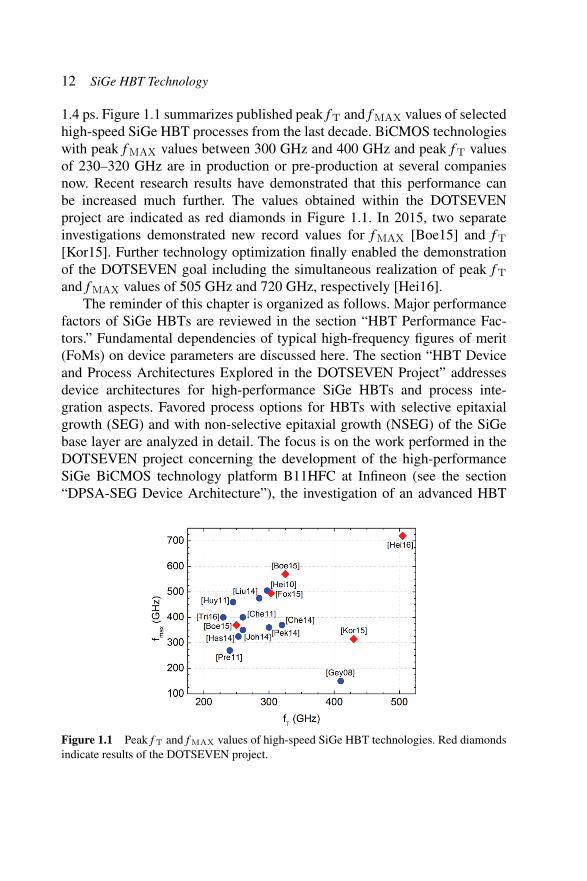
1.4 ps. Figure 1.1 summarizes published peak f T and f MAX values of selectedhigh-speed SiGe HBT processes from the last decade. BiCMOS technologieswith peak f MAX values between 300 GHz and 400 GHz and peak f T valuesof 230–320 GHz are in production or pre-production at several companiesnow. Recent research results have demonstrated that this performance canbe increased much further. The values obtained within the DOTSEVENproject are indicated as red diamonds in Figure 1.1. In 2015, two separateinvestigations demonstrated new record values for f MAX [Boe15] and f T
[Kor15]. Further technology optimization finally enabled the demonstrationof the DOTSEVEN goal including the simultaneous realization of peak f T
and f MAX values of 505 GHz and 720 GHz, respectively [Hei16].The reminder of this chapter is organized as follows. Major performance
factors of SiGe HBTs are reviewed in the section “HBT Performance Fac-tors.” Fundamental dependencies of typical high-frequency figures of merit(FoMs) on device parameters are discussed here. The section “HBT Deviceand Process Architectures Explored in the DOTSEVEN Project” addressesdevice architectures for high-performance SiGe HBTs and process inte-gration aspects. Favored process options for HBTs with selective epitaxialgrowth (SEG) and with non-selective epitaxial growth (NSEG) of the SiGebase layer are analyzed in detail. The focus is on the work performed in theDOTSEVEN project concerning the development of the high-performanceSiGe BiCMOS technology platform B11HFC at Infineon (see the section“DPSA-SEG Device Architecture”), the investigation of an advanced HBT
Figure 1.1 Peak f T and f MAX values of high-speed SiGe HBT technologies. Red diamondsindicate results of the DOTSEVEN project.
1.2 HBT Performance Factors 13
process with SEG of the base and epitaxial base link (EBL) regions (see thesection “Approaches to Overcome Limitations of the DPSA-SEG Architec-ture”), and the optimization of a process with NSEG of the base (see thesection “Non-selective Epitaxial Growth of the Base”), which was finallyutilized by IHP to reach the DOTSEVEN goal. The section “Optimization ofthe Vertical Doping Profile” addresses the optimization of the vertical dopingprofile for f T improvement. The final technology optimization for minimumdevice parasitics and balanced f T and f MAX improvement is discussed in thesection “Optimization towards 700 GHz f MAX.”
1.2 HBT Performance Factors
Typical FoMs characterizing a process technology in terms of high-frequencyperformance are the transit frequency f T and the maximum oscillation fre-quency f MAX. The transit frequency f T is defined as the frequency for whichthe small-signal current gain |h21|falls to unity, i.e.,
|h21 (f)|f=fT= 1. (1.1)
The frequency f MAX is defined as the maximum frequency for which thetransistor can amplify power. In this context, Mason’s unilateral power gainU is widely used, and f MAX is defined by:
U (f)|f=fMAX= 1. (1.2)
While the frequency f MAX represents a speed metric for circuits such asamplifiers and oscillators, f T gives a measure of the speed of switchingcircuits such as dividers. Ring-oscillator gate delays are relevant FoMs fordigital high-speed circuits. Here, we use the current mode logic (CML)ring-oscillator gate delay time τCML. In addition, the base–collector break-down voltage BVCEs and the open-base emitter–collector breakdown voltageBVCEo are important since they determine the maximum output power thatcan be provided by a transistor. Further characteristics of relevance for eval-uating potential applications include the minimum noise figure, the linearity,and the gain of a transistor.
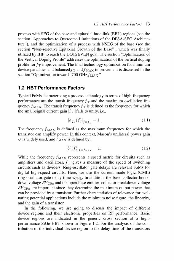
In the following, we are going to discuss the impact of differentdevice regions and their electronic properties on RF performance. Basicdevice regions are indicated in the generic cross section of a high-performance SiGe HBT shown in Figure 1.2. For the analysis of the con-tribution of the individual device region to the delay time of the transistors
14 SiGe HBT Technology
Figure 1.2 Schematic cross section of a high speed SiGe HBT.
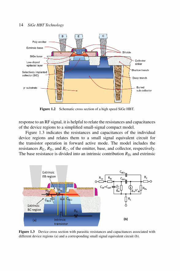
response to an RF signal, it is helpful to relate the resistances and capacitancesof the device regions to a simplified small-signal compact model.
Figure 1.3 indicates the resistances and capacitances of the individualdevice regions and relates them to a small signal equivalent circuit forthe transistor operation in forward active mode. The model includes theresistances RE, RB, and RC, of the emitter, base, and collector, respectively.The base resistance is divided into an intrinsic contribution RBi and extrinsic
Figure 1.3 Device cross section with parasitic resistances and capacitances associated withdifferent device regions (a) and a corresponding small signal equivalent circuit (b).
1.2 HBT Performance Factors 15
contribution RBx originating from the link region which contacts the intrinsicbase. The base–collector capacitance (CBC) is divided into an intrinsic partCBCi and an extrinsic part CBCx related to the base link region. CBE includesthe depletion capacitance as well as the oxide capacitance of the base–emitterjunction, Cdiff is the diffusion capacitance related to the storage of minoritycharges in the forward operation mode, βf is the forward DC current gain,gm is the transconductance, REa is the output resistance related to the Earlyeffect, and V’BE is the intrinsic base–emitter voltage.
The frequency-dependent small signal current gain h21(f ) of the modeldepicted in Figure 1.3 is approximately given by:
1
h21 (f)=
1
βf+ j2πf
(Cdiff + CBE + CBC
gm+ (RE +RC)CBC
). (1.3)
In the limit of large frequencies, h21 is inversely proportional to the frequencyf. The corresponding unit gain transit frequency f T is given as:
1
2πfT=Cdiff + CBE + CBC
gm+ (RE +RC)CBC. (1.4)
The transconductance gm is proportional to the collector current IC in thebias region of ideal exponential slope according to gm = qIC/kBT , where qis the elementary charge, kB is Boltzmann’s constant, and T is the junctiontemperature. The diffusion capacitance Cdiff accounts for the storage oflocally compensated minority carriers during forward transistor operation.The contribution to Cdiff can be analyzed in a charge-control model [Tau98].This analysis relies on the fact that any variation of the bias point of the deviceis related to changes of the carrier densities within the device which are fedby currents into the device contacts. The corresponding forward transit time
τF =Cdiff
gm= τE + τEB + τB + τBC (1.5)
can be divided into contributions accounting for charge storage in the emitter,base–emitter junction, base, and base–collector junction regions, respectively.According to the charge-control model, these contributions are approximatelygiven by:
τE =CE
gm, (1.6)
τEB =CN
gm, (1.7)
16 SiGe HBT Technology
τB =w2
B
2DnB+wB
vsat, (1.8)
τBC =wBC
2vsat. (1.9)
Here, wB is the width of the neutral base region, wBC is the depletion widthof the base–collector junction, DnB is the electron diffusion coefficient in thebase, and vsat is the saturation velocity of electrons. CE and CN denotethe parts of the diffusion capacitance related to neutral charge storage inthe emitter and base–emitter junction regions, respectively. The compensatedcharge CN stored in the base–emitter junction can account for a significantcontribution to τF in particular at high current densities [Hue96]. The emitterdelay time τE is of minor importance for typical SiGe HBTs since the amountof holes stored in the emitter is inversely proportional to the current gain.The magnitude of CE is determined by the emitter properties. The maximumoscillation frequency of the equivalent circuit of Figure 1.3 is approximatelygiven by:
fMAX∼=
√fT
8π ((RBx +RBi)CBi +RBxCBx). (1.10)
This relation is reduced to:
fMAX∼=√
fT
8πRBCBC, (1.11)
if RB and CBC are not separated into extrinsic and intrinsic contributions.Based on the Equations (1.4) to (1.10), the following scenario can be
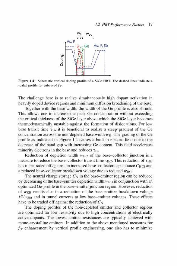
envisioned for the enhancement of the cutoff frequencies f T and f MAX byscaling vertical and lateral device dimensions. The transit frequency f T ispredominantly determined by the vertical doping profile. Figure 1.4 illustratesqualitatively the directions of profile optimization for f T enhancement.
Reduction of the width wB of the boron-doped base reduces the basetransit time τB according to Equation (1.7). A minimum width of the boron-doped region has to be ensured together with a low base sheet resistance.Today, base layers with typical sheet resistances of about 2 kΩ/sq can begrown epitaxially with widths of less than 5 nm. In addition to the depositionof a thin base, its diffusion during subsequent processes has to be kept assmall as possible. A widely applied approach to minimize B diffusion isthe additional doping of the SiGe layer with carbon [Lan96, Ost97, Rue99].Moreover, the thermal budget of post-epi processing has to be kept low.
1.2 HBT Performance Factors 17
Figure 1.4 Schematic vertical doping profile of a SiGe HBT. The dashed lines indicate ascaled profile for enhanced f T.
The challenge here is to realize simultaneously high dopant activation inheavily doped device regions and minimum diffusion broadening of the base.
Together with the base width, the width of the Ge profile is also shrunk.This allows one to increase the peak Ge concentration without exceedingthe critical thickness of the SiGe layer above which the SiGe layer becomesthermodynamically unstable against the formation of dislocations. For lowbase transit time τB, it is beneficial to realize a steep gradient of the Geconcentration across the non-depleted base width wB. The grading of the Geprofile as indicated in Figure 1.4 causes a built-in electric field due to thedecrease of the band gap with increasing Ge content. This field acceleratesminority electrons in the base and reduces τB.
Reduction of depletion width wBC of the base–collector junction is ameasure to reduce the base–collector transit time τBC. This reduction of τBC
has to be traded off against an increased base–collector capacitance CBCi anda reduced base–collector breakdown voltage due to reduced wBC.
The neutral charge storage CN in the base–emitter region can be reducedby decreasing of the base–emitter depletion width wEB in conjunction with anoptimized Ge-profile in the base–emitter junction region. However, reductionof wEB results also in a reduction of the base–emitter breakdown voltageBV EB0 and in tunnel currents at low base–emitter voltages. These effectshave to be traded off against the reduction of CN.
The doping profiles of the non-depleted emitter and collector regionsare optimized for low resistivity due to high concentrations of electricallyactive dopants. The lowest emitter resistances are typically achieved withmono-crystalline emitters. In addition to the above mentioned measures forf T enhancement by vertical profile engineering, one also has to minimize
18 SiGe HBT Technology
contributions to the base–emitter and base–collector capacitances originatingfrom the edges of the device for realizing higher f T values according toEquation (1.4).
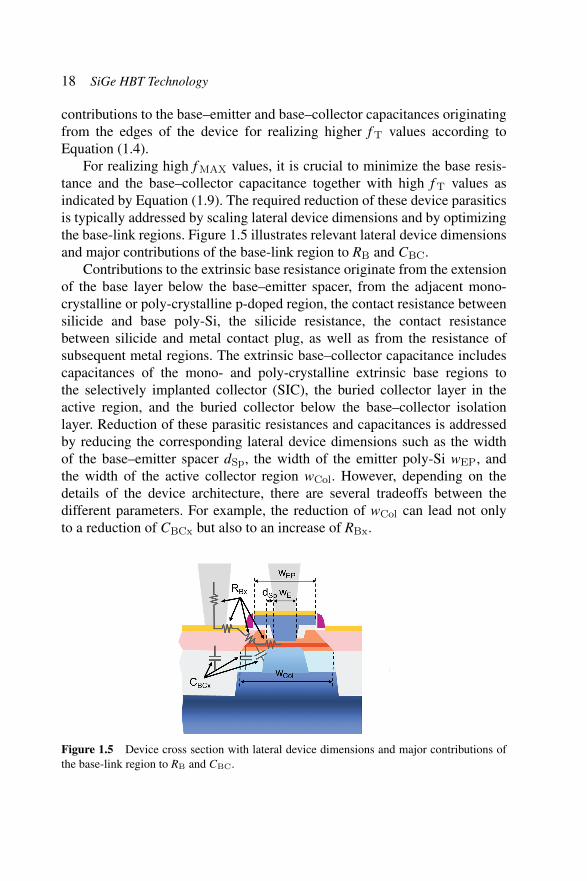
For realizing high f MAX values, it is crucial to minimize the base resis-tance and the base–collector capacitance together with high f T values asindicated by Equation (1.9). The required reduction of these device parasiticsis typically addressed by scaling lateral device dimensions and by optimizingthe base-link regions. Figure 1.5 illustrates relevant lateral device dimensionsand major contributions of the base-link region to RB and CBC.
Contributions to the extrinsic base resistance originate from the extensionof the base layer below the base–emitter spacer, from the adjacent mono-crystalline or poly-crystalline p-doped region, the contact resistance betweensilicide and base poly-Si, the silicide resistance, the contact resistancebetween silicide and metal contact plug, as well as from the resistance ofsubsequent metal regions. The extrinsic base–collector capacitance includescapacitances of the mono- and poly-crystalline extrinsic base regions tothe selectively implanted collector (SIC), the buried collector layer in theactive region, and the buried collector below the base–collector isolationlayer. Reduction of these parasitic resistances and capacitances is addressedby reducing the corresponding lateral device dimensions such as the widthof the base–emitter spacer dSp, the width of the emitter poly-Si wEP, andthe width of the active collector region wCol. However, depending on thedetails of the device architecture, there are several tradeoffs between thedifferent parameters. For example, the reduction of wCol can lead not onlyto a reduction of CBCx but also to an increase of RBx.
Figure 1.5 Device cross section with lateral device dimensions and major contributions ofthe base-link region to RB and CBC.
1.3 HBT Device and Process Architectures Explored in the DOTSEVEN 19
The intrinsic contribution to the base resistance RBi can be reduced for agiven base sheet resistance Rsbi by narrowing the emitter window width wE.In a typical scaling scenario, lateral scaling of wE is accompanied by verticalscaling of the doping profile and increased current densities at peak f T. Underthese conditions, it is a major challenge to maintain low emitter and collectorresistances as well as thermal resistances when the emitter width is scaleddown.
Scaling of the HBT device dimensions under the boundary conditions ofminimum base, emitter, and collector resistances imposes complex require-ments on device architecture and fabrication process. These challengeshave stimulated various innovations of the HBT fabrication process whichaddressed the reduction of the individual device parasitics by structuralimprovements as well as by improved material properties such as reducedspecific and contact resistances. Approaches explored in the DOTSEVENproject will be reviewed in the following sections.
1.3 HBT Device and Process Architectures Exploredin the DOTSEVEN Project
Innovations of the device architecture and of the fabrication processes havebeen major factors for the improvement of the RF performance of SiGe HBTsduring the last decades. Fundamental requirements on the device architec-ture for high-speed HBTs are minimum access resistances to the intrinsicemitter, base, and collector regions together with low contributions of theextrinsic device regions to the base–collector and base–emitter capacitances.The development of device and process architectures which facilitate thesimultaneous realization of low RB and low CBC has been a major challengein this context. The realization of devices with low thermal resistances is afurther requirement in order to limit self-heating.
The above-mentioned device targets have to be realized in fabricationprocesses which are manufacturable in high volumes with high yield. Afurther fundamental requirement on the HBT fabrication process is thecompatibility with the addressed CMOS technology platform. The integra-tion of SiGe HBTs and other RF-enabling passive or active devices into aBiCMOS technology platform has to be realized without degrading HBTor CMOS device characteristics or yield. The large potential of advancedCMOS processes for geometry scaling opens new options also for the HBTfabrication. However, new challenges arise for the integration of SiGe HBTs
20 SiGe HBT Technology
in continuously shrinking CMOS nodes from tight constraints on the thermalbudget and on device topology.
As regards the SiGe HBT device concepts, all current production-relatedhigh-speed transistors take advantage of the so-called double-poly-Si (DP)architecture. This configuration provides access from the contact region tothe intrinsic base and emitter region by poly-Si layers which are dielectricallyisolated against the surrounding transistor regions. It is a powerful meansto keep extrinsic parasitics, such as RBx, CBCx, RE, and CBE, small. It istherefore evident that the basic structure of modern SiGe HBTs is becomingmore similar. Nevertheless, we are faced with quite different approaches fordevice manufacturing resulting in different consequences of their potentialelectrical performance.
A key differentiator for SiGe HBT fabrication is the way in which theSiGe base is formed. Existing SiGe HBT technologies use either selective ornon-selective epitaxial growth of the base. Both approaches have been usedfor the development of high-performance SiGe HBT processes and foundtheir way into industrial mass production. In the DOTFIVE project, tech-nological solutions were developed promising further speed enhancementsfor HBT concepts with selective as well as with non-selective base epitaxy.Due to their specific implications on the process complexity and the self-alignment of the transistor regions, various technologies were investigatedalso in the DOTSEVEN project using the different base-epitaxy methods.Opportunities and challenges of the two approaches will be discussed in detailin the following subsections. This applies also to process options regardingthe lateral collector isolation by deep trenches or by the standard shallowtrenches of the CMOS process, the formation of the highly conductive sub-collector, and the formation of the base–emitter structure. The choice of thesubstrate, i.e., bulk or silicon-on-insulator (SOI), is another criterion to dif-ferentiate SiGe HBT technologies. Driven by the continuous development ofSOI-based CMOS technologies several publications have been devoted to theissue of a suitable technology and device concept for high-speed SiGe HBTson SOI wafers [Was00, Rue04, Ave05, Thi13]. Here, we will not addressthis architectural aspect because it was outside the focus of the DOTSEVENproject.
1.3.1 Selective Epitaxial Growth of the Base
The classical DP-self-aligned (SA) SiGe HBT technology with SEG of thebase represents the most attractive process architecture from the point ofview of manufacturing and degree of self-alignment. As described in the next
1.3 HBT Device and Process Architectures Explored in the DOTSEVEN 21
section, the DOTFIVE project partners Infineon and STMicroelectronics aswell as FreeScale (now NXP) worked intensively on this concept in the lastdecade to push its performance. However, substantial improvements beyondthe current level will hardly be feasible with this approach as discussed in thesection “Approaches to Overcome Limitations of the DPSA-SEG Architec-ture.” In the DOTFIVE project, alternative SEG process flows were developedto overcome limitations of the conventional DPSA-SEG technology. It willbe reported below in detail on joint activities of Infineon and IHP in theDOTSEVEN project to test one of these approaches within Infineon’s 130 nmBiCMOS platform.
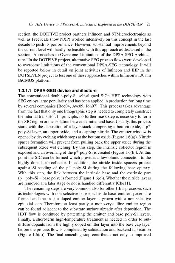
1.3.1.1 DPSA-SEG device architectureThe conventional double-poly-Si self-aligned SiGe HBT technology withSEG enjoys large popularity and has been applied in production for long timeby several companies [Boe04, Ave09, Joh07]. This process takes advantagefrom the fact that only one lithographic step is needed to completely constructthe internal transistor. In principle, no further mask step is necessary to formthe SIC region or the isolation between emitter and base. Usually, this processstarts with the deposition of a layer stack comprising a bottom oxide, a p+
poly-Si layer, an upper oxide, and a capping nitride. The emitter window isopened by dry etching which stops at the bottom oxide (Figure 1.6(a)). Nitridespacer formation will prevent from pulling back the upper oxide during thesubsequent oxide wet etching. By this step, the intrinsic collector region isexposed and an overhang of the p+ poly-Si is created (Figure 1.6(b)). At thispoint the SIC can be formed which provides a low-ohmic connection to thehighly doped sub-collector. In addition, the nitride inside spacers protectagainst Si seeding of the p+ poly-Si during the following base epitaxy.With this step, the link between the intrinsic base and the extrinsic part(p+ poly-Si = base poly) is formed (Figure 1.6(c)). Whether the nitride layersare removed at a later stage or not is handled differently [Che11].
The remaining steps are very common also for other HBT processes suchas technologies with non-selective base epi. Inside base–emitter spacers areformed and the in situ doped emitter layer is grown with a non-selectiveepitaxial step. Therefore, at least partly, a mono-crystalline emitter regioncan be found adjacent to the substrate surface already after deposition. TheHBT flow is continued by patterning the emitter and base poly-Si layers.Finally, a short-term high-temperature treatment is needed in order to out-diffuse dopants from the highly doped emitter layer into the base cap layerbefore the process flow is completed by salicidation and backend fabrication(Figure 1.6(d)). The final annealing step contributes not only to improved
22 SiGe HBT Technology
Figure 1.6 Schematic cross sections of conventional DPSA-SEG process flow.
base-current idealities but it also determines the emitter resistance. In the caseof a bipolar-only technology, e.g., Infineon’s B7HF200 [Boe04], the thermalbudget is largely governed by the needs of the HBT. In BiCMOS processes,as a rule, the minimum requirements of the source–drain anneal determine thecrucial thermal budget of the HBT assuming that a ‘source/drain-after-HBT’integration scheme is realized.
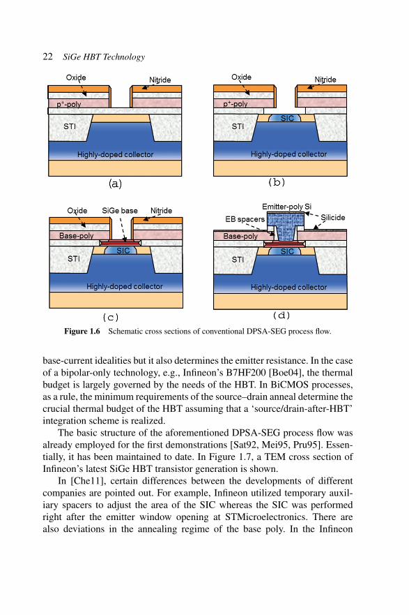
The basic structure of the aforementioned DPSA-SEG process flow wasalready employed for the first demonstrations [Sat92, Mei95, Pru95]. Essen-tially, it has been maintained to date. In Figure 1.7, a TEM cross section ofInfineon’s latest SiGe HBT transistor generation is shown.
In [Che11], certain differences between the developments of differentcompanies are pointed out. For example, Infineon utilized temporary auxil-iary spacers to adjust the area of the SIC whereas the SIC was performedright after the emitter window opening at STMicroelectronics. There arealso deviations in the annealing regime of the base poly. In the Infineon
1.3 HBT Device and Process Architectures Explored in the DOTSEVEN 23
Figure 1.7 TEM cross section of a DPSA-SEG HBT of Infineon’s B11HFC technology[Boe15].
flow, an extra thermal treatment after base epitaxy is introduced for out-diffusing B from the base poly toward the intrinsic base layer. Consequently,the base resistance can be reduced but the base tends to broaden causinglower f T values. Nevertheless, variations of this annealing showed room foroptimizations to increase f MAX with tolerable constrains for f T [Can12].
The collector construction used by Hitachi [Has14], Infineon [Boe15],and STMicroelectronics [Che14] includes all elements which are typical fora high-speed Si bipolar transistor: an epitaxially buried, highly doped sub-collector isolated laterally by deep trenches and a low-ohmic connectionto the collector contact realized by a so-called collector sinker. In order tosave fabrication efforts and to reduce complexity of the BiCMOS process,NXP (former FreeScale) developed a Sub-Isolation Buried Layer (SIBL)collector structure using only shallow trench isolation (STI) [Joh07]. Acommon feature of all these technologies is the shallow-trench isolation (STI)between the internal transistor region and the collector contact which enablessimultaneously a low capacitive base link.
In the DOTFIVE project comprehensive efforts were made by Infineonand STMicroelectronics to improve the high-frequency behavior of the con-ventional DPSA-SEG technology as reported in [Che11]. Clear progress wasachieved by changing the vertical profile, thermal treatments, as well as thelateral transistor dimensions. At that time, Infineon was able to increase its
24 SiGe HBT Technology
initial f T/f MAX values of 190 GHz/250 GHz (B7HF200, [Boe04]) finallyto 230 GHz/350 GHz while STMicroelectronics increased these FoMs from230 GHz/280 GHz (BiMOS9MW, [Ave09]) to 260 GHz/400 GHz. Later,both companies could demonstrate this performance level in a BiCMOSenvironment too. The f MAX results obtained in the DOTFIVE project andin the recent past for the DPSA-SEG concept [Has14, Che14, Tri16] indicatethat it is difficult to reach values beyond 400 GHz. The limited possibilitiesto decrease RBx have been proved as the key bottleneck for advancements ofthe overall RF performance. Alternative concepts which were conceived toovercome this issue will be presented in the next subsection.
1.3.1.2 Approaches to overcome limitations of the DPSA-SEGarchitecture
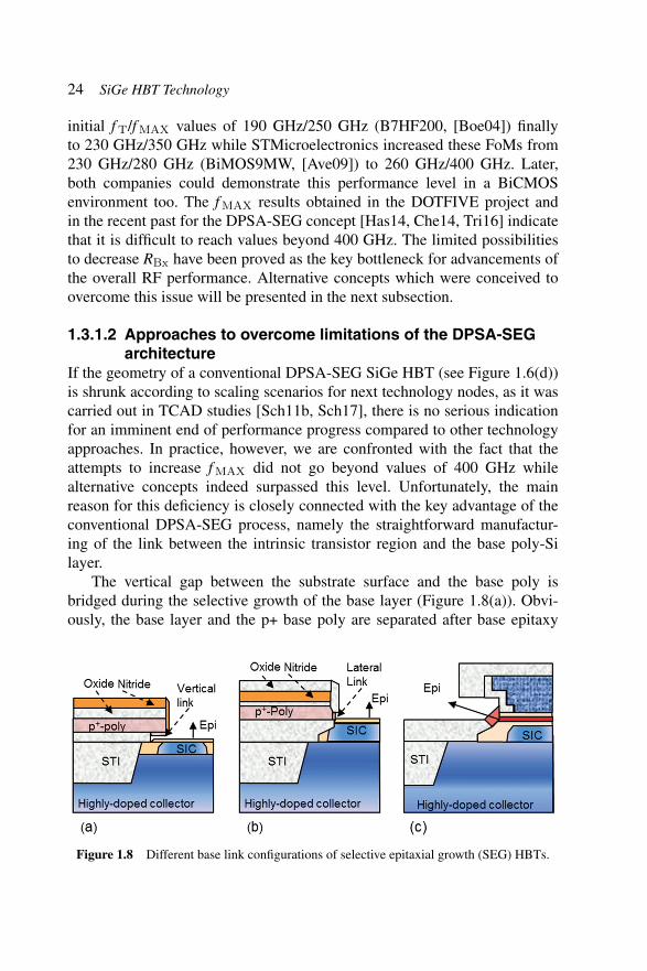
If the geometry of a conventional DPSA-SEG SiGe HBT (see Figure 1.6(d))is shrunk according to scaling scenarios for next technology nodes, as it wascarried out in TCAD studies [Sch11b, Sch17], there is no serious indicationfor an imminent end of performance progress compared to other technologyapproaches. In practice, however, we are confronted with the fact that theattempts to increase f MAX did not go beyond values of 400 GHz whilealternative concepts indeed surpassed this level. Unfortunately, the mainreason for this deficiency is closely connected with the key advantage of theconventional DPSA-SEG process, namely the straightforward manufactur-ing of the link between the intrinsic transistor region and the base poly-Silayer.
The vertical gap between the substrate surface and the base poly isbridged during the selective growth of the base layer (Figure 1.8(a)). Obvi-ously, the base layer and the p+ base poly are separated after base epitaxy
Figure 1.8 Different base link configurations of selective epitaxial growth (SEG) HBTs.
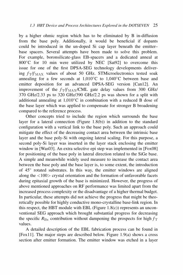
1.3 HBT Device and Process Architectures Explored in the DOTSEVEN 25
by a higher ohmic region which has to be eliminated by B in-diffusionfrom the base poly. Additionally, it would be beneficial if dopantscould be introduced in the un-doped Si cap layer beneath the emitter–base spacers. Several attempts have been made to solve this problem.For example, boronsilicate-glass EB-spacers and a dedicated anneal at800C for 10 min were utilized by NEC [Sat92] to overcome thisissue for one of the first DPSA-SEG technology developments deliver-ing f T/f MAX values of about 50 GHz. STMicroelectronics tested soakannealing for a few seconds at 1,010C to 1,040C between base andemitter deposition for an advanced DPSA-SEG version [Can12]. Animprovement of the f T/f MAX/CML gate delay values from 300 GHz/370 GHz/2.33 ps to 320 GHz/390 GHz/2.2 ps was shown for a split withadditional annealing at 1,010C in combination with a reduced B dose ofthe base layer which was applied to compensate for stronger B broadeningcompared to the reference process.
Other concepts tried to include the region which surrounds the baselayer for a lateral connection (Figure 1.8(b)) in addition to the standardconfiguration with a vertical link to the base poly. Such an approach couldmitigate the effect of the decreasing contact area between the intrinsic baselayer and the base poly-Si with ongoing lateral scaling. For this purpose, asecond poly-Si layer was inserted in the layer stack enclosing the emitterwindow in [Was03]. An extra selective epi step was implemented in [Fox08]for positioning of the base poly in lateral direction related to the SiGe base.A simple and meanwhile widely used measure to increase the contact areabetween the base poly and the base layer is, to some extent, the introductionof 45 rotated substrates. In this way, the emitter windows are alignedalong the <100> crystal orientation and the formation of unfavorable facetsduring epitaxial growth of the base is minimized. However, the progress ofabove mentioned approaches on RF performance was limited apart from theincreased process complexity or the disadvantage of a higher thermal budget.In particular, these attempts did not achieve the progress that might be theo-retically possible for highly conductive mono-crystalline base-link region. Inthis respect, the HBT module with EBL (Figure 1.8(c)) represents an uncon-ventional SEG approach which brought substantial progress for decreasingthe specific RBx contribution without dampening the prospects for high f T
values.A detailed description of the EBL fabrication process can be found in
[Fox11]. The major steps are described below. Figure 1.9(a) shows a crosssection after emitter formation. The emitter window was etched in a layer
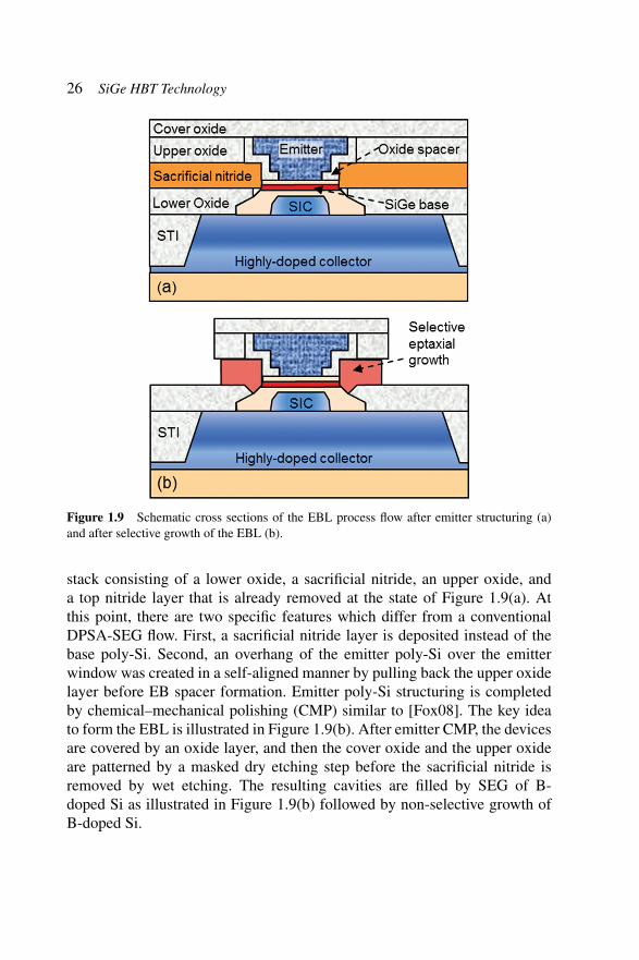
26 SiGe HBT Technology
Figure 1.9 Schematic cross sections of the EBL process flow after emitter structuring (a)and after selective growth of the EBL (b).
stack consisting of a lower oxide, a sacrificial nitride, an upper oxide, anda top nitride layer that is already removed at the state of Figure 1.9(a). Atthis point, there are two specific features which differ from a conventionalDPSA-SEG flow. First, a sacrificial nitride layer is deposited instead of thebase poly-Si. Second, an overhang of the emitter poly-Si over the emitterwindow was created in a self-aligned manner by pulling back the upper oxidelayer before EB spacer formation. Emitter poly-Si structuring is completedby chemical–mechanical polishing (CMP) similar to [Fox08]. The key ideato form the EBL is illustrated in Figure 1.9(b). After emitter CMP, the devicesare covered by an oxide layer, and then the cover oxide and the upper oxideare patterned by a masked dry etching step before the sacrificial nitride isremoved by wet etching. The resulting cavities are filled by SEG of B-doped Si as illustrated in Figure 1.9(b) followed by non-selective growth ofB-doped Si.
1.3 HBT Device and Process Architectures Explored in the DOTSEVEN 27
In the first publication on this technology concept [Fox11] f T/f MAX/CMLgate delay values of 300 GHz/480 GHz/1.9 ps were presented. However, adetailed comparison of the EBL HBT performance against standard DPSA-SEG results was not in the focus of this first demonstration. This assess-ment has been addressed in the DOTSEVEN project. The EBL HBT wascompared directly with the conventional DPSA-SEG approach based onidentical collector designs, transistor layouts, and measurement conditions.For this purpose, the EBL HBT module was implemented in Infineon’s0.13 µm BiCMOS environment which includes the standard collector con-cept of an epitaxially buried sub-collector and deep-trench (DT) isolationcombined with a mm-wave Cu back-end-of-line (BEOL). In contrast, theoriginal EBL process comprised IHP’s DT-free collector approach [Hei02]using STI-isolated, highly doped collector regions as well as an Al-basedBEOL.
For this exercise, EBL HBTs and conventional DPSA-SEG HBTs werecompared in two ways. First, IHP manufactured its novel device on Infineonwafers in a bipolar-only flow. The joint fabrication started at Infineon byforming the buried sub-collector, the deep trench and STI, and the MOS gates(Table 1.1). Then, the wafer processing was continued at IHP with the EBLmodule. The CMOS fabrication steps after the HBT module, which coulddeteriorate the HBT performance, were skipped in these experiments. Allprocess steps for the bipolar devices including the final activation annealingand salicidation were done in these runs at IHP. Compared to [Fox11], theemitter–base spacer process was slightly modified to assist the formation ofreduced emitter widths. To eliminate the risk of poly-Si residues, an extramask was introduced to remove the emitter poly-Si outside of the transistorregions before emitter planarization. Otherwise, we preserved the originalEBL flow including the thermal treatment and doping of the SIC, SiGe base,and emitter.
In a second cycle, the full BiCMOS flow was applied. The HBT fab-rication was finished at IHP with removing the CMOS protection layer.The further processing corresponded to Infineon’s 0.13-µm BiCMOS pro-cess including low-doped-drain implantation and annealing, CMOS gatespacer deposition, source/drain implantation and annealing, and salicidation.Table 1.1 shows which process modules were carried out by Infineon andwhich by IHP for the bipolar-only flow and for the full BiCMOS process,respectively.
28 SiGe HBT Technology
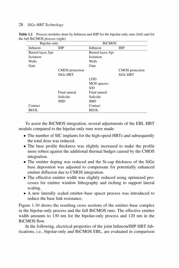
Table 1.1 Process modules done by Infineon and IHP for the bipolar-only runs (left) and forthe full BiCMOS process (right)
Bipolar-only BiCMOSInfineon IHP Infineon IHPBuried layer, Epi Buried layer, EpiIsolation IsolationWells WellsGate Gate
CMOS protection CMOS protectionSiGe HBT SiGe HBT
LDDMOS spacersS/D
Final anneal Final annealSalicide SalicideIMD IMD
Contact ContactBEOL BEOL
To assist the BiCMOS integration, several adjustments of the EBL HBTmodule compared to the bipolar-only runs were made:
• The number of SIC implants for the high-speed HBTs and subsequentlythe total dose was reduced.• The base profile thickness was slightly increased to make the profile
more robust against the additional thermal budget caused by the CMOSintegration.• The emitter doping was reduced and the Si-cap thickness of the SiGe
base deposition was adjusted to compensate for potentially enhancedemitter diffusion due to CMOS integration.• The effective emitter width was slightly reduced using optimized pro-
cesses for emitter window lithography and etching to support lateralscaling.• A new laterally scaled emitter–base spacer process was introduced to
reduce the base link resistance.
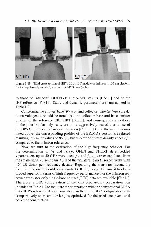
Figure 1.10 shows the resulting cross sections of the emitter–base complexin the bipolar-only process and the full BiCMOS runs. The effective emitterwidth amounts to 130 nm for the bipolar-only process and 120 nm in theBiCMOS flow.
In the following, electrical properties of the joint Infineon/IHP HBT fab-rications, i.e., bipolar-only and BiCMOS EBL, are evaluated in comparison
1.3 HBT Device and Process Architectures Explored in the DOTSEVEN 29
Figure 1.10 TEM cross section of IHP’s EBL-HBT module on Infineon’s 130 nm platformfor the bipolar-only run (left) and full BiCMOS flow (right).
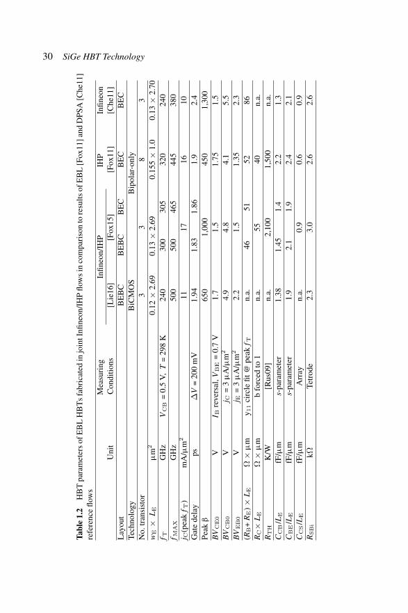
to those of Infineon’s DOTFIVE DPSA-SEG results [Che11] and of theIHP reference [Fox11]. Static and dynamic parameters are summarized inTable 1.2.
Concerning the emitter–base (BVEB0) and collector–base (BVCB0) break-down voltages, it should be noted that the collector–base and base–emitterprofiles of the reference EBL HBT [Fox11], and consequently also thoseof the joint bipolar-only runs, are more aggressively scaled than those ofthe DPSA reference transistor of Infineon [Che11]. Due to the modificationslisted above, the corresponding profiles of the BiCMOS version are relaxedresulting in similar values of BVEB0 but also of the current density at peak f T
compared to the Infineon reference.Now, we turn to the evaluation of the high-frequency behavior. For
the determination of f T and f MAX, OPEN and SHORT de-embeddeds-parameters up to 50 GHz were used. f T and f MAX are extrapolated fromthe small-signal current gain |h21|and the unilateral gain U, respectively, with–20 dB decay per frequency decade. Regarding the transistor layout, thefocus will be on the double-base contact (BEBC) design because it has beenproved superior in terms of high-frequency performance. For the Infineon ref-erence transistor only single-base contact (BEC) data are available [Che11].Therefore, a BEC configuration of the joint bipolar-only preparation wasincluded in Table 1.2 to facilitate the comparison with the conventional DPSAdata. IHP’s reference device consists of an 8-emitter BEC configuration withcomparatively short emitter lengths optimized for the used unconventionalcollector construction.
30 SiGe HBT Technology
Tab
le1.2
HB
Tpa
ram
eter
sof
EB
LH
BT
sfa
bric
ated
injo
intI
nfine
on/I
HP
flow
sin
com
pari
son
tore
sults
ofE
BL
[Fox
11]a
ndD
PSA
[Che
11]
refe
renc
eflo
ws
Mea
suri
ngIn
fineo
n/IH
PIH
PIn
fineo
nU
nit
Con
ditio
ns[L
ie16
][F
ox15
][F
ox11
][C
he11
]L
ayou
tB
EB
CB
EB
CB
EC
BE
CB
EC
Tech
nolo
gyB
iCM
OS
Bip
olar
-onl
yN
o.tr
ansi
stor
33
83
wE×
LE
µm
20.
12×
2.69
0.13
×2.
690.
155×
1.0
0.13
×2.
70f T
GH
zV
CB
=0.
5V
,T
=29
8K
240
300
305
320
240
f MAX
GH
z50
050
046
544
538
0j C
(pea
kf T
)m
A/µ
m2
1117
1610
Gat
ede
lay
ps∆
V=
200
mV
1.94
1.83
1.86
1.9
2.4
Peak
β65
01,
000
450
1,30
0B
VCE0
VI B
reve
rsal
,VBE
=0.
7V
1.7
1.5
1.75
1.5
BV
CB0
Vj C
=3
µA
/µm
24.
94.
84.
15.
5B
VEB0
Vj E
=3
µA
/µm
22.
21.
51.
352.
3(R
B+
RE
)×
LE
Ω×
µm
y 11
circ
lefit
@pe
akf T
n.a.
4651
5286
RC×
LE
Ω×
µm
bfo
rced
to1
n.a.
5540
n.a.
RTH
K/W
[Rus
09]
n.a.
2,10
01,
500
n.a.
CCB
/LE
fF/µ
ms-
para
met
er1.
381.
451.
42.
21.
3C
BE
/LE
fF/µ
ms-
para
met
er1.
92.
11.
92.
42.
1C
CS
/LE
fF/µ
mA
rray
n.a.
0.9
0.6
0.9
RSBi
kΩTe
trod
e2.
33.
02.
62.
6
1.3 HBT Device and Process Architectures Explored in the DOTSEVEN 31
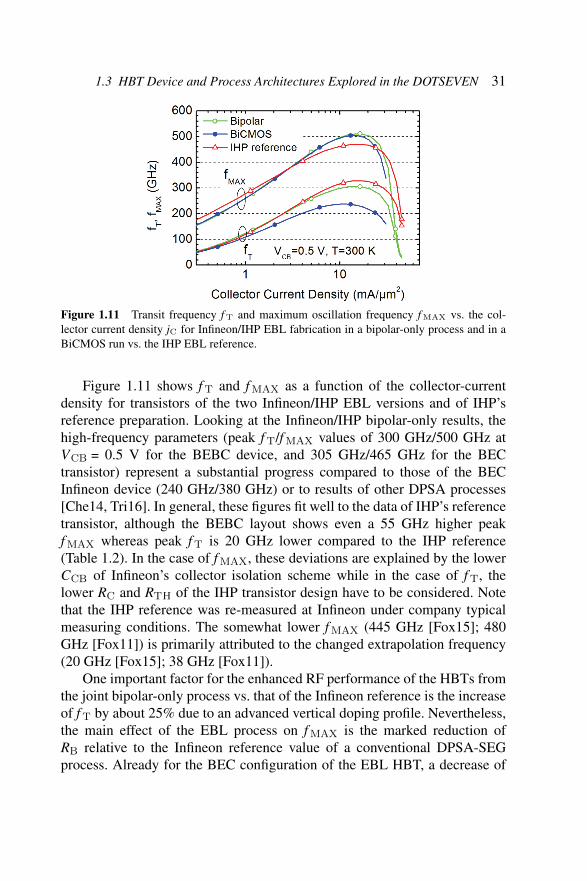
Figure 1.11 Transit frequency f T and maximum oscillation frequency f MAX vs. the col-lector current density jC for Infineon/IHP EBL fabrication in a bipolar-only process and in aBiCMOS run vs. the IHP EBL reference.
Figure 1.11 shows f T and f MAX as a function of the collector-currentdensity for transistors of the two Infineon/IHP EBL versions and of IHP’sreference preparation. Looking at the Infineon/IHP bipolar-only results, thehigh-frequency parameters (peak f T/f MAX values of 300 GHz/500 GHz atVCB = 0.5 V for the BEBC device, and 305 GHz/465 GHz for the BECtransistor) represent a substantial progress compared to those of the BECInfineon device (240 GHz/380 GHz) or to results of other DPSA processes[Che14, Tri16]. In general, these figures fit well to the data of IHP’s referencetransistor, although the BEBC layout shows even a 55 GHz higher peakf MAX whereas peak f T is 20 GHz lower compared to the IHP reference(Table 1.2). In the case of f MAX, these deviations are explained by the lowerCCB of Infineon’s collector isolation scheme while in the case of f T, thelower RC and RTH of the IHP transistor design have to be considered. Notethat the IHP reference was re-measured at Infineon under company typicalmeasuring conditions. The somewhat lower f MAX (445 GHz [Fox15]; 480GHz [Fox11]) is primarily attributed to the changed extrapolation frequency(20 GHz [Fox15]; 38 GHz [Fox11]).
One important factor for the enhanced RF performance of the HBTs fromthe joint bipolar-only process vs. that of the Infineon reference is the increaseof f T by about 25% due to an advanced vertical doping profile. Nevertheless,the main effect of the EBL process on f MAX is the marked reduction ofRB relative to the Infineon reference value of a conventional DPSA-SEGprocess. Already for the BEC configuration of the EBL HBT, a decrease of
32 SiGe HBT Technology
the length-specific input resistance (RB + RE) by 40% relative to the Infineonreference is observed. Similar relations are true also of the BEBC BiCMOSdevice. It should be stressed at this point again how important identicalRF transistor layouts, measurement tools, and extraction procedures are forreliable evaluations. For example, (RB + RE) values given in Table 1.2 areextracted from y11 circle fit. This leads to 17% lower values compared to theprocedure applied in [Fox 11] based on a circular fit of s11.
Considering the high-frequency behavior of the HBTs, promising resultswere demonstrated with respect to a reduced base link resistance. However,the f T of 240 GHz realized for the EBL module within Infineon’s 130 nmBiCMOS platform is significantly below the ambitious targets for next SiGeHBT generation. Certainly, the effect of a higher thermal budget of the post-HBT BiCMOS steps at Infineon compared to those of the original IHP flowhas to be considered. In addition, more aggressive EB and BC doping profileshave to be applied for further f T enhancement.
It remains the question whether there are architecture- or flow-related rea-sons which make it more difficult or impossible to approach the performancevalues presented in the section “Optimization towards 700 GHz f MAX” forthe NSEG HBT also with the EBL concept. However, the finally achievedenhanced high-frequency parameters of the NSEG HBT were paid partiallywith increased process complexity. The search for an HBT architecture andcorresponding process flow which combine best performance and reliable,cost-effective processing is in this context of continuing interest.
1.3.2 Non-selective Epitaxial Growth of the Base
Non-selective epitaxial growth of the SiGe base layer is widely usedin SiGe HBT fabrication. Examples are production processes of IBM/Globalfoundries [Orn03, Pek14] and TowerJazz [Pre11] as well as severaltechnology generations developed by IHP [Kno04, Hei07, Rue10] and byNXP and imec [Don07, Huy11]. These processes have in common a layerstack consisting of a Si buffer layer, a SiGe layer containing the boron-dopedbase, and a Si cap layer deposited across the whole wafer. This layer stackgrows mono-crystalline in active HBT areas where the Si surface is exposedwhile it grows poly-crystalline in all other areas covered with oxide or nitride.This so-called differential growth mode is in contrast to the SEG where thedeposition occurs only in the exposed Si regions.
An implication of the non-selective growth mode is that the poly-crystalline layer which is grown on the isolation layers adjacent to the activeHBT can be used to form the extrinsic base regions. Typically this approach
1.3 HBT Device and Process Architectures Explored in the DOTSEVEN 33
is combined with an additional ion implantation into the extrinsic baseregions to enhance their conductivity. This approach was applied, e.g., in the0.25-µm BiCMOS process SG25H1 of IHP which provides peak f T/f MAX
values of 180 GHz/220 GHz [Hei07]. In such an approach, the thickness ofthe extrinsic base is defined by the layer stack grown to form the intrinsicbase. This limits the achievable sheet resistance of the extrinsic base and inparticular the conductivity of the extrinsic base region below the poly-emitteroverhang. That is why several approaches have been developed to enhancethe conductivity of the extrinsic base region by deposition of additional Silayers. It turned out that those elevated extrinsic base regions were necessaryfor extending f MAX of NSEG HBTs beyond 300 GHz. An NSEG processwith elevated extrinsic base regions self-aligned to the emitter window isused, e.g., in IBM’s 90 nm SiGe BiCMOS technology [Pek14] exhibitingpeak f T/f MAX values of 300 GHz/360 GHz. In a variant of the process, theRF performance could be further improved to f T/f MAX of 285 GHz/475 GHzwith the help of millisecond annealing [Liu14].
An alternative NSEG HBT process with elevated extrinsic base regionsis used in IHP’s 130 nm BiCMOS technology [Rue10, Rue12]. This HBTconcept was the starting point for the performance optimization toward500 GHz f MAX performed in the DOTFIVE project. It turned out to bea promising concept for even further performance improvement in theDOTSEVEN project. In the following, we review the main features of thecorresponding HBT process flow. The elevated extrinsic base regions areformed by an additional epitaxial step after emitter structuring as first pub-lished in [Rue03]. The implementation described below corresponds to thetechnology SG13G2 of IHP offering HBTs with f T/f MAX /gate-delay valuesof 300 GHz/450 GHz/2.0 ps.
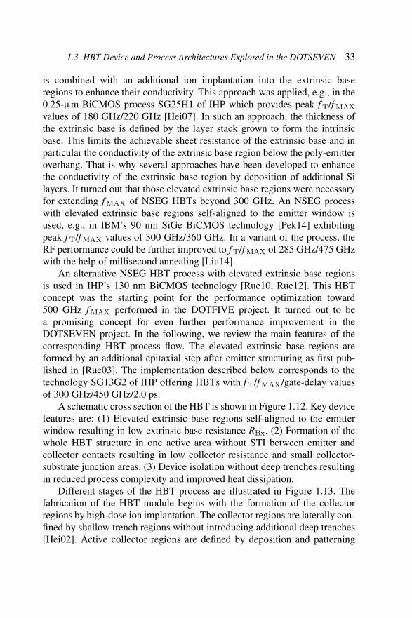
A schematic cross section of the HBT is shown in Figure 1.12. Key devicefeatures are: (1) Elevated extrinsic base regions self-aligned to the emitterwindow resulting in low extrinsic base resistance RBx. (2) Formation of thewhole HBT structure in one active area without STI between emitter andcollector contacts resulting in low collector resistance and small collector-substrate junction areas. (3) Device isolation without deep trenches resultingin reduced process complexity and improved heat dissipation.
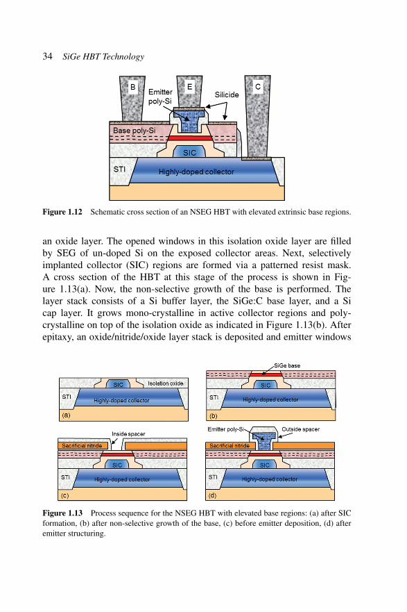
Different stages of the HBT process are illustrated in Figure 1.13. Thefabrication of the HBT module begins with the formation of the collectorregions by high-dose ion implantation. The collector regions are laterally con-fined by shallow trench regions without introducing additional deep trenches[Hei02]. Active collector regions are defined by deposition and patterning
34 SiGe HBT Technology
Figure 1.12 Schematic cross section of an NSEG HBT with elevated extrinsic base regions.
an oxide layer. The opened windows in this isolation oxide layer are filledby SEG of un-doped Si on the exposed collector areas. Next, selectivelyimplanted collector (SIC) regions are formed via a patterned resist mask.A cross section of the HBT at this stage of the process is shown in Fig-ure 1.13(a). Now, the non-selective growth of the base is performed. Thelayer stack consists of a Si buffer layer, the SiGe:C base layer, and a Sicap layer. It grows mono-crystalline in active collector regions and poly-crystalline on top of the isolation oxide as indicated in Figure 1.13(b). Afterepitaxy, an oxide/nitride/oxide layer stack is deposited and emitter windows
Figure 1.13 Process sequence for the NSEG HBT with elevated base regions: (a) after SICformation, (b) after non-selective growth of the base, (c) before emitter deposition, (d) afteremitter structuring.
1.3 HBT Device and Process Architectures Explored in the DOTSEVEN 35
are structured. Additional inside spacers are formed before depositing andstructuring the As-doped emitter. Figure 1.13(c) shows the device crosssection before emitter deposition. The emitter is capped with a dielectric layerand structured via a patterned resist mask. Outside spacers are formed onthe emitter resulting in the device structure shown in Figure 1.13(d). Next, thesacrificial nitride layer is removed by wet etching followed by the selectivegrowth of the B-doped elevated extrinsic base regions. The fabrication ofthe HBT module is continued with the patterning of the base poly-Si layervia a further resist mask. After the described process sequence for HBTstructuring, the devices are exposed to a final rapid thermal processing (RTP)step which is used in the BiCMOS flow for the activation of source anddrain regions. In the reference technology SG13G2 a spike anneal at 1,050Cis applied for this purpose. Finally, cobalt salicidation is performed on allcontact areas and the aluminum metallization is processed. A schematic crosssection of the final HBT structure is depicted in Figure 1.12.
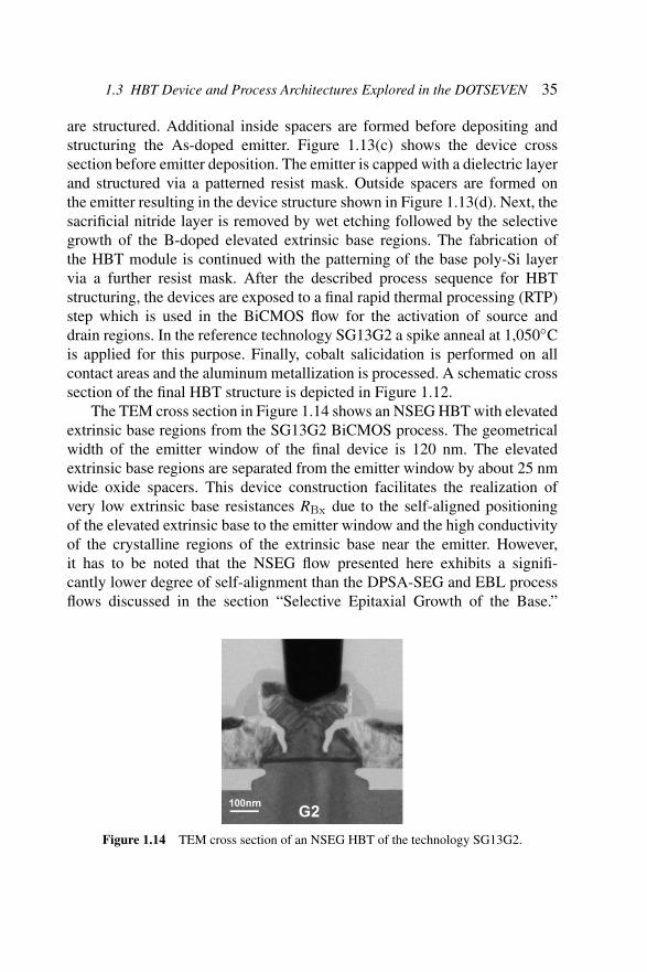
The TEM cross section in Figure 1.14 shows an NSEG HBT with elevatedextrinsic base regions from the SG13G2 BiCMOS process. The geometricalwidth of the emitter window of the final device is 120 nm. The elevatedextrinsic base regions are separated from the emitter window by about 25 nmwide oxide spacers. This device construction facilitates the realization ofvery low extrinsic base resistances RBx due to the self-aligned positioningof the elevated extrinsic base to the emitter window and the high conductivityof the crystalline regions of the extrinsic base near the emitter. However,it has to be noted that the NSEG flow presented here exhibits a signifi-cantly lower degree of self-alignment than the DPSA-SEG and EBL processflows discussed in the section “Selective Epitaxial Growth of the Base.”
Figure 1.14 TEM cross section of an NSEG HBT of the technology SG13G2.

36 SiGe HBT Technology
In particular, the collector window, the SIC implantation, the emitter window,and the emitter poly overhang are not self-aligned to each other. Their relativealignment is defined by the alignment accuracy of the respective lithographicmask steps. This sensitivity to the accuracy of the lithographic alignment canimpose severe limitation for further scaling of lateral device dimensions.
Regardless of the above-mentioned limitations of the described NSEGHBT process with respect to self-alignment and scalability, it served asworkhorse for optimizing the HBT performance by IHP within the projectsDOTFIVE and DOTSEVEN. This arose from the greater experience andfamiliarity with the NSEG HBT compared to concepts with selective epitaxydiscussed above. The fabrication of the NSEG HBT in the SG13G2 BiCMOSprocess resulted from intensive optimization of this transistor concept withinthe DOTFIVE project [Hei10]. This raises the question if and by what meansfurther potential performance improvements could be achieved. Accordingto device simulation, there are still respectable reserves for speed increase[Sch11a, Sch11b]. In particular, lateral scaling should help to increase f MAX
further. In addition, an appropriate vertical scaling of the doping and Geprofile is required for the desired objective of balanced high f T and f MAX
values.
1.4 Optimization of the Vertical Doping Profile
Optimized device architectures as well as lateral and vertical scaling con-tributed to noticeable progress for f MAX over the last years. In contrast, thepotential for improving f T seemed to be limited, in particular, if high f MAX
values have to be retained. All successful attempts to push the peak f T of SiGeHBTs beyond 350 GHz delivered rather low f MAX values. For example, theSiGe HBT which demonstrated the highest fT until 2015 showed a peak fT
value of 410 GHz together with a peak f MAX value of 190 GHz [Gey08].Within the DOTSEVEN project, we considered two directions toward
HBT performance optimization. First, we focused on aggressive scaling ofvertical HBT doping and Ge profiles for increased f T. Second, a devicearchitecture and process flow with a balanced f T-f MAX design at highestperformance level was aimed for. In the following, we describe the mainresults of the experiments for f T optimization.
Various vertical doping and Ge profiles were investigated in a simplifiedHBT flow described in [Kor15]. In these experiments, a reduced thermalbudget of the HBT process was utilized for limiting dopant diffusion. Lat-eral device dimensions were relaxed with respect to the reference process
1.4 Optimization of the Vertical Doping Profile 37
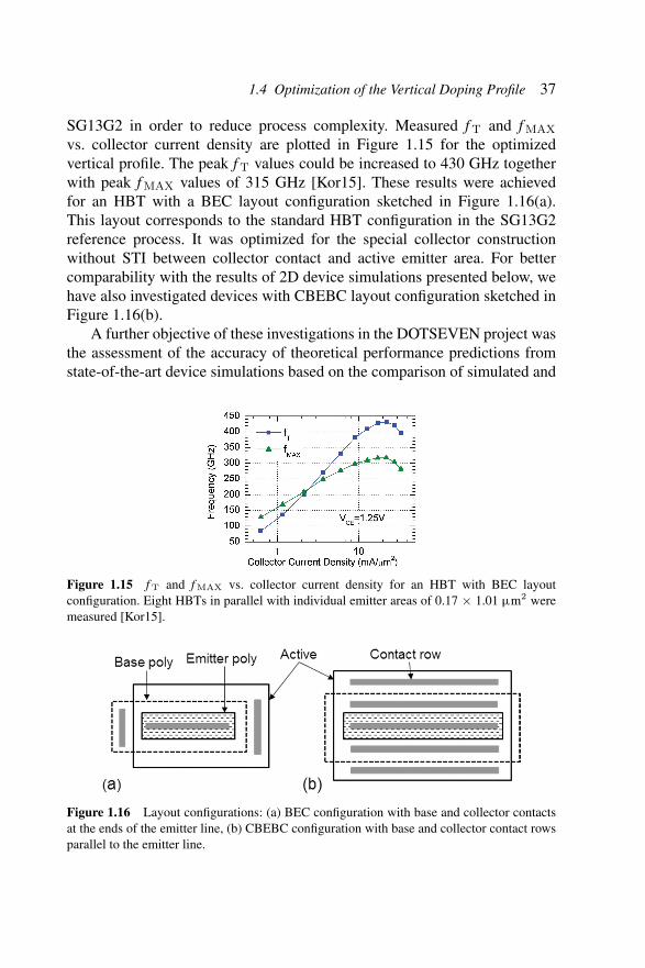
SG13G2 in order to reduce process complexity. Measured f T and f MAX
vs. collector current density are plotted in Figure 1.15 for the optimizedvertical profile. The peak f T values could be increased to 430 GHz togetherwith peak f MAX values of 315 GHz [Kor15]. These results were achievedfor an HBT with a BEC layout configuration sketched in Figure 1.16(a).This layout corresponds to the standard HBT configuration in the SG13G2reference process. It was optimized for the special collector constructionwithout STI between collector contact and active emitter area. For bettercomparability with the results of 2D device simulations presented below, wehave also investigated devices with CBEBC layout configuration sketched inFigure 1.16(b).
A further objective of these investigations in the DOTSEVEN project wasthe assessment of the accuracy of theoretical performance predictions fromstate-of-the-art device simulations based on the comparison of simulated and
Figure 1.15 f T and f MAX vs. collector current density for an HBT with BEC layoutconfiguration. Eight HBTs in parallel with individual emitter areas of 0.17 × 1.01 µm2 weremeasured [Kor15].
Figure 1.16 Layout configurations: (a) BEC configuration with base and collector contactsat the ends of the emitter line, (b) CBEBC configuration with base and collector contact rowsparallel to the emitter line.
38 SiGe HBT Technology
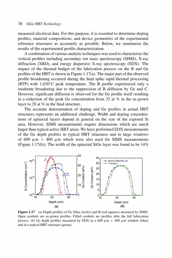
measured electrical data. For this purpose, it is essential to determine dopingprofiles, material compositions, and device geometries of the experimentalreference structures as accurately as possible. Below, we summarize theresults of the experimental profile characterization.
A combination of various analytic techniques was used to characterize thevertical profiles including secondary ion mass spectroscopy (SIMS), X-raydiffraction (XRD), and energy dispersive X-ray spectroscopy (EDX). Theimpact of the thermal budget of the fabrication process on the B and Geprofiles of the HBT is shown in Figure 1.17(a). The major part of the observedprofile broadening occurred during the final spike rapid thermal processing(RTP) with 1,030C peak temperature. The B profile experienced only amoderate broadening due to the suppression of B diffusion by Ge and C.However, significant diffusion is observed for the Ge profile itself resultingin a reduction of the peak Ge concentration from 32 at % in the as-grownlayer to 28 at % in the final structure.
The accurate determination of doping and Ge profiles in actual HBTstructures represents an additional challenge. Width and doping concentra-tions of epitaxial layers depend in general on the size of the exposed Siarea. However, SIMS measurements require dimensions which are muchlarger than typical active HBT areas. We have performed EDX measurementsof the Ge depth profiles in typical HBT structures and in large windowsof 600 µm × 400 µm which were also used for SIMS measurements(Figure 1.17(b)). The width of the epitaxial SiGe layer was found to be 14%
Figure 1.17 (a) Depth profiles of Ge (blue circles) and B (red squares) measured by SIMS.Open symbols are as-grown profiles. Filled symbols are profiles after the full fabricationprocess. (b) Ge depth profiles measured by EDX in a 600 µm × 400 µm window (blue)and in a typical HBT structure (green).
1.4 Optimization of the Vertical Doping Profile 39
smaller in the small HBT window while about the same peak Ge concentra-tions were measured in both structures. The Ge profile of the small windowcan be obtained from the Ge profile in the SIMS monitor by shrinking thedepth scale by 14%. We assume that the same shrink of the depth scale appliesto the B profile resulting in a 14% thinner profile in the small HBT window.
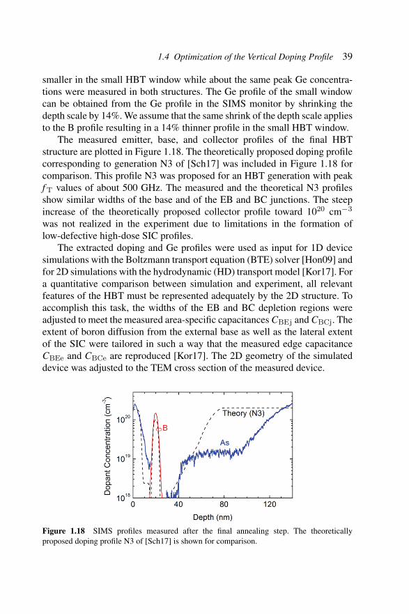
The measured emitter, base, and collector profiles of the final HBTstructure are plotted in Figure 1.18. The theoretically proposed doping profilecorresponding to generation N3 of [Sch17] was included in Figure 1.18 forcomparison. This profile N3 was proposed for an HBT generation with peakf T values of about 500 GHz. The measured and the theoretical N3 profilesshow similar widths of the base and of the EB and BC junctions. The steepincrease of the theoretically proposed collector profile toward 1020 cm−3
was not realized in the experiment due to limitations in the formation oflow-defective high-dose SIC profiles.
The extracted doping and Ge profiles were used as input for 1D devicesimulations with the Boltzmann transport equation (BTE) solver [Hon09] andfor 2D simulations with the hydrodynamic (HD) transport model [Kor17]. Fora quantitative comparison between simulation and experiment, all relevantfeatures of the HBT must be represented adequately by the 2D structure. Toaccomplish this task, the widths of the EB and BC depletion regions wereadjusted to meet the measured area-specific capacitances CBEj and CBCj. Theextent of boron diffusion from the external base as well as the lateral extentof the SIC were tailored in such a way that the measured edge capacitanceCBEe and CBCe are reproduced [Kor17]. The 2D geometry of the simulateddevice was adjusted to the TEM cross section of the measured device.
Figure 1.18 SIMS profiles measured after the final annealing step. The theoreticallyproposed doping profile N3 of [Sch17] is shown for comparison.
40 SiGe HBT Technology
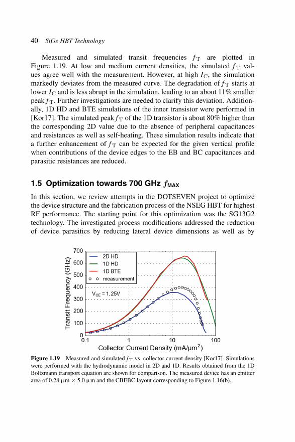
Measured and simulated transit frequencies f T are plotted inFigure 1.19. At low and medium current densities, the simulated f T val-ues agree well with the measurement. However, at high IC, the simulationmarkedly deviates from the measured curve. The degradation of f T starts atlower IC and is less abrupt in the simulation, leading to an about 11% smallerpeak f T. Further investigations are needed to clarify this deviation. Addition-ally, 1D HD and BTE simulations of the inner transistor were performed in[Kor17]. The simulated peak f T of the 1D transistor is about 80% higher thanthe corresponding 2D value due to the absence of peripheral capacitancesand resistances as well as self-heating. These simulation results indicate thata further enhancement of f T can be expected for the given vertical profilewhen contributions of the device edges to the EB and BC capacitances andparasitic resistances are reduced.
1.5 Optimization towards 700 GHz fMAX
In this section, we review attempts in the DOTSEVEN project to optimizethe device structure and the fabrication process of the NSEG HBT for highestRF performance. The starting point for this optimization was the SG13G2technology. The investigated process modifications addressed the reductionof device parasitics by reducing lateral device dimensions as well as by
Figure 1.19 Measured and simulated f T vs. collector current density [Kor17]. Simulationswere performed with the hydrodynamic model in 2D and 1D. Results obtained from the 1DBoltzmann transport equation are shown for comparison. The measured device has an emitterarea of 0.28 µm × 5.0 µm and the CBEBC layout corresponding to Figure 1.16(b).
1.5 Optimization towards 700 GHz fMAX 41
improving the control of the doping profile and the conductivity of criticaldevice regions.
The possibilities for lateral scaling of the emitter window by lithographicmeasures were already largely exhausted in the SG13G2 technology due tothe resolution limits of the DUV tool at IHP. A further challenge for down-scaling of the emitter window width is the fabrication of conformal insidespacers in narrow emitter windows. This concerns in particular the depositionof homogenous dielectric layers with good step coverage and the reactive ionetching with minimum damage of the Si surface. Finally, we had to learnfrom a series of development loops that the room for a well-controlled down-scaling of the emitter width was very limited within the current process flow.Starting from a value of 120 nm in SG13G2, the emitter width was reducedto 100 nm in an intermediate process variant (split CR2). For the final deviceoptimization, an emitter width of 105 nm was realized.
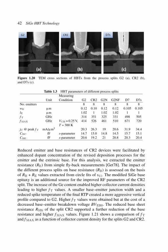
First, we discuss the process stage that was used for circuit fabricationin the DOTSEVEN project. After using the SG13G2 technology for a firstcircuit fabrication run, an HBT process with improved RF performance wastargeted for a second circuit fabrication run (CR2). The following processchanges were addressed in this split: smaller emitter–base spacers and smalleremitter window widths were formed by modifying the corresponding depo-sition and etching processes. An emitter deposition process with enhancedAs concentration previously explored in [Hei10] was introduced. The dopingconcentration of the epitaxially elevated base link regions was enhancedand a new base profile was applied. In addition to these measures whichare compatible with the SG13G2 BiCMOS process, we explored for furtheroptimization of the HBT performance process changes which are in conflictwith the reference BiCMOS flow. The thickness of the cobalt silicide wasincreased and the thickness of the silicide blocking spacer at the sidewall ofthe emitter poly-Si was reduced to minimize the external base resistance. Thepeak temperature of the final RTP step was reduced in order to minimizediffusion broadening of the base and consequently the base transit time. TheHBT cross sections depicted in Figure 1.20 indicate the decreased emitterwindow width, the reduced widths of the base–emitter and silicide blockingspacers, and the enhanced CoSi2 thickness of the split CR2 with respect tothe reference process SG13G2 (G2).
Electrical device parameters for the investigated process variants aresummarized in Table 1.3. The process developments introduced in the CR2split resulted in significant improvements of f T, f MAX, and the CML ringoscillator gate delay compared to the reference process G2 (Table 1.3).
42 SiGe HBT Technology
Figure 1.20 TEM cross sections of HBTs from the process splits G2 (a), CR2 (b),and D7s (c).
Table 1.3 HBT parameters of different process splitsMeasuring
Unit Condition G2 CR2 G2N G2NF D7 D7sNo. emitters 8 8 8 8 8 8wE µm 0.12 0.10 0.12 0.12 0.105 0.105lE µm 1.02 1 1.02 1.02 1 1f T GHz 314 351 325 331 498 505f MAX GHz VCB = 0.25 V,
T = 300 K414 526 461 510 671 720
jC @ peak f T mA/µm2 20.3 26.3 19 20.6 31.9 34.4CBC fF s-parameter 14.7 15.0 14.8 14.5 15.7 15.1CBE fF s-parameter 20.6 19.2 21 20.8 20.3 20.4
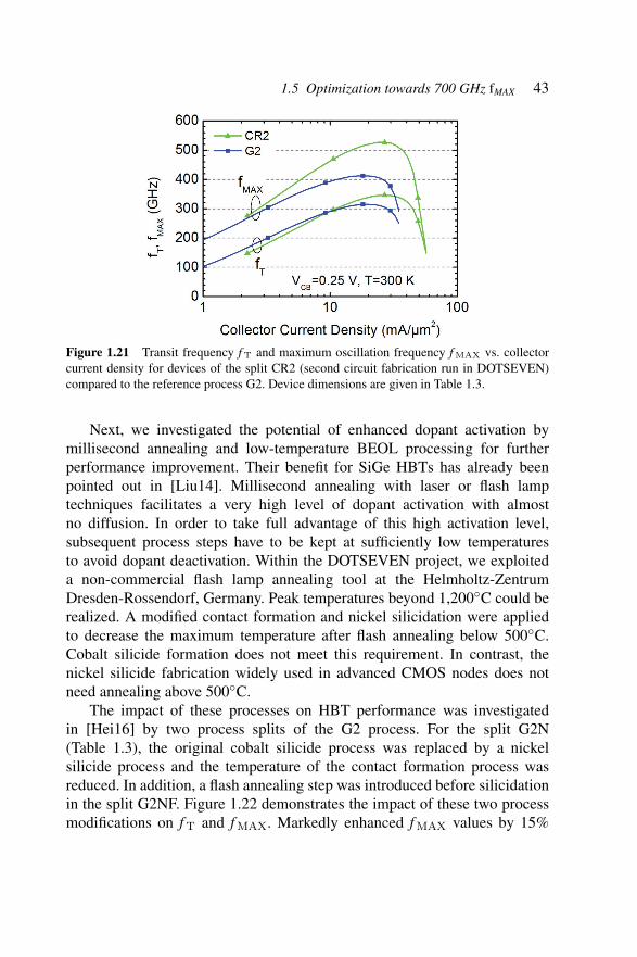
Reduced emitter and base resistances of CR2 devices were facilitated byenhanced dopant concentration of the revised deposition processes for theemitter and the extrinsic base. For this analysis, we extracted the emitterresistance (RE) from simple fly-back measurements [Get78]. The impact ofthe different process splits on base resistance (RB) is assessed on the basisof RB + RE values extracted from circle fits of s11. The modified SiGe baseepitaxy is an additional source for the improved RF parameters of the CR2split. The increase of the Ge content enabled higher collector current densitiesleading to higher f T values. A smaller base–emitter junction width and areduced spike temperature of the final RTP created a more aggressive verticalprofile compared to G2. Higher f T values were obtained but at the cost of adecreased base–emitter breakdown voltage BVEB0. The reduced base sheetresistance RSBi of the split CR2 supported a further reduction of the baseresistance and higher f MAX values. Figure 1.21 shows a comparison of f T
and f MAX as a function of collector current density for the splits G2 and CR2.
1.5 Optimization towards 700 GHz fMAX 43
Figure 1.21 Transit frequency f T and maximum oscillation frequency f MAX vs. collectorcurrent density for devices of the split CR2 (second circuit fabrication run in DOTSEVEN)compared to the reference process G2. Device dimensions are given in Table 1.3.
Next, we investigated the potential of enhanced dopant activation bymillisecond annealing and low-temperature BEOL processing for furtherperformance improvement. Their benefit for SiGe HBTs has already beenpointed out in [Liu14]. Millisecond annealing with laser or flash lamptechniques facilitates a very high level of dopant activation with almostno diffusion. In order to take full advantage of this high activation level,subsequent process steps have to be kept at sufficiently low temperaturesto avoid dopant deactivation. Within the DOTSEVEN project, we exploiteda non-commercial flash lamp annealing tool at the Helmholtz-ZentrumDresden-Rossendorf, Germany. Peak temperatures beyond 1,200C could berealized. A modified contact formation and nickel silicidation were appliedto decrease the maximum temperature after flash annealing below 500C.Cobalt silicide formation does not meet this requirement. In contrast, thenickel silicide fabrication widely used in advanced CMOS nodes does notneed annealing above 500C.
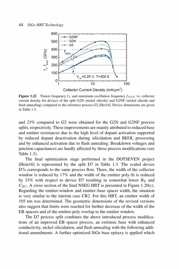
The impact of these processes on HBT performance was investigatedin [Hei16] by two process splits of the G2 process. For the split G2N(Table 1.3), the original cobalt silicide process was replaced by a nickelsilicide process and the temperature of the contact formation process wasreduced. In addition, a flash annealing step was introduced before silicidationin the split G2NF. Figure 1.22 demonstrates the impact of these two processmodifications on f T and f MAX. Markedly enhanced f MAX values by 15%
44 SiGe HBT Technology
Figure 1.22 Transit frequency f T and maximum oscillation frequency f MAX vs. collectorcurrent density for devices of the split G2N (nickel silicide) and G2NF (nickel silicide andflash annealing) compared to the reference process G2 [Hei16]. Device dimensions are givenin Table 1.3.
and 23% compared to G2 were obtained for the G2N and G2NF processsplits, respectively. These improvements are mainly attributed to reduced baseand emitter resistances due to the high level of dopant activation supportedby reduced dopant deactivation during silicidation and BEOL processingand by enhanced activation due to flash annealing. Breakdown voltages andjunction capacitances are hardly affected by these process modifications (seeTable 1.3).
The final optimization stage performed in the DOTSEVEN project[Hein16] is represented by the split D7 in Table 1.3. The scaled deviceD7s corresponds to the same process flow. There, the width of the collectorwindow is reduced by 17% and the width of the emitter poly-Si is reducedby 33% with respect to device D7 resulting in somewhat lower RB andCBC. A cross section of the final NSEG HBT is presented in Figure 1.20(c).Regarding the emitter-window and emitter–base spacer width, the situationis very similar to the interim case CR2. For this HBT, an emitter width of105 nm was determined. The geometric dimensions of the revised versionsalso suggest that limits were reached for further decrease of the width of theEB spacers and of the emitter-poly overlap to the emitter window.
The D7 process split combines the above introduced process modifica-tions of an improved EB spacer process, an extrinsic base with enhancedconductivity, nickel silicidation, and flash annealing with the following addi-tional amendments. A further optimized SiGe base epitaxy is applied which
1.5 Optimization towards 700 GHz fMAX 45
closely resembles the B and Ge profiles of the f T-optimized device describedin the section “Optimization of the Vertical Doping Profile.” The thicknessesof the lower doped parts of the emitter–base and base–collector junctions arereduced with respect to split CR2. The emitter utilizes the enhanced dopinglevel but now with reduced layer thickness. Furthermore, the fabricationprocess for the SIC was revised. In the G2 HBT flow, the SIC was formedwith the help of a patterned resist mask. In the D7 split, this process sequencewas replaced by a hard mask with inside spacers. By this means, we gainedadditional flexibility in matching the lateral dimensions of the SIC and theemitter window. The implantation dose of the SIC was doubled in the splitD7 with respect to the reference process G2.
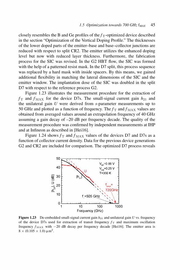
Figure 1.23 illustrates the measurement procedure for the extraction off T and f MAX for the device D7s. The small-signal current gain h21 andthe unilateral gain U were derived from s-parameter measurements up to50 GHz and plotted as a function of frequency. The f T and f MAX values areobtained from averaged values around an extrapolation frequency of 40 GHzassuming a gain decay of –20 dB per frequency decade. The quality of themeasurement procedure was confirmed by independent measurements at IHPand at Infineon as described in [Hei16].
Figure 1.24 shows f T and f MAX values of the devices D7 and D7s as afunction of collector current density. Data for the previous device generationsG2 and CR2 are included for comparison. The optimized D7 process reveals
Figure 1.23 De-embedded small-signal current gain h21 and unilateral gain U vs. frequencyof the device D7s used for extraction of transit frequency f T and maximum oscillationfrequency f MAX with −20 dB decay per frequency decade [Hei16]. The emitter area is8 × (0.105 × 1.0) µm2.
46 SiGe HBT Technology
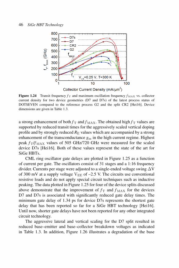
Figure 1.24 Transit frequency f T and maximum oscillation frequency f MAX vs. collectorcurrent density for two device geometries (D7 and D7s) of the latest process status ofDOTSEVEN compared to the reference process G2 and the split CR2 [Hei16]. Devicedimensions are given in Table 1.3.
a strong enhancement of both f T and f MAX. The obtained high f T values aresupported by reduced transit times for the aggressively scaled vertical dopingprofile and by strongly reduced RE values which are accompanied by a strongenhancement of the transconductance gm in the high current regime. Highestpeak f T/f MAX values of 505 GHz/720 GHz were measured for the scaleddevice D7s [Hei16]. Both of these values represent the state of the art forSiGe HBTs.
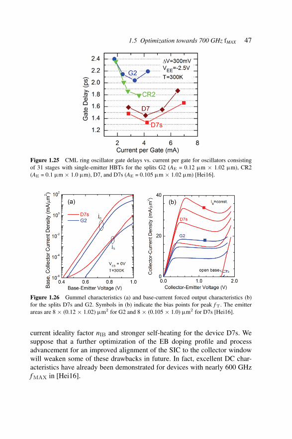
CML ring oscillator gate delays are plotted in Figure 1.25 as a functionof current per gate. The oscillators consist of 31 stages and a 1:16 frequencydivider. Currents per stage were adjusted to a single-ended voltage swing ∆Vof 300 mV at a supply voltage VEE of –2.5 V. The circuits use conventionalresistive loads and do not apply special circuit techniques such as inductivepeaking. The data plotted in Figure 1.25 for four of the device splits discussedabove demonstrate that the improvement of f T and f MAX for the devicesD7 and D7s is associated with significantly reduced gate delay times. Theminimum gate delay of 1.34 ps for device D7s represents the shortest gatedelay that has been reported so far for a SiGe HBT technology [Hei16].Until now, shorter gate delays have not been reported for any other integratedcircuit technology.
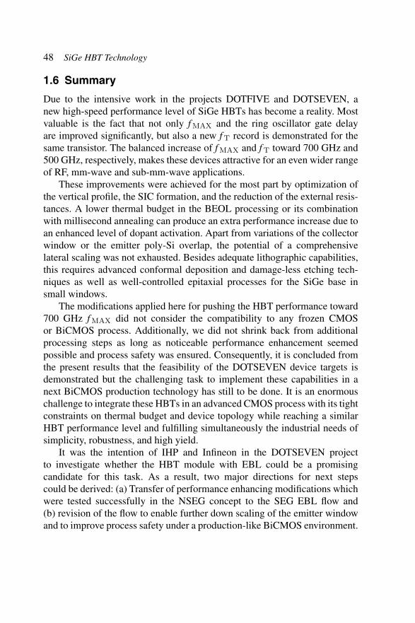
The aggressive lateral and vertical scaling for the D7 split resulted inreduced base–emitter and base–collector breakdown voltages as indicatedin Table 1.3. In addition, Figure 1.26 illustrates a degradation of the base
1.5 Optimization towards 700 GHz fMAX 47
Figure 1.25 CML ring oscillator gate delays vs. current per gate for oscillators consistingof 31 stages with single-emitter HBTs for the splits G2 (AE = 0.12 µm × 1.02 µm), CR2(AE = 0.1 µm × 1.0 µm), D7, and D7s (AE = 0.105 µm × 1.02 µm) [Hei16].
Figure 1.26 Gummel characteristics (a) and base-current forced output characteristics (b)for the splits D7s and G2. Symbols in (b) indicate the bias points for peak f T. The emitterareas are 8 × (0.12 × 1.02) µm2 for G2 and 8 × (0.105 × 1.0) µm2 for D7s [Hei16].
current ideality factor nIB and stronger self-heating for the device D7s. Wesuppose that a further optimization of the EB doping profile and processadvancement for an improved alignment of the SIC to the collector windowwill weaken some of these drawbacks in future. In fact, excellent DC char-acteristics have already been demonstrated for devices with nearly 600 GHzf MAX in [Hei16].
48 SiGe HBT Technology
1.6 Summary
Due to the intensive work in the projects DOTFIVE and DOTSEVEN, anew high-speed performance level of SiGe HBTs has become a reality. Mostvaluable is the fact that not only f MAX and the ring oscillator gate delayare improved significantly, but also a new f T record is demonstrated for thesame transistor. The balanced increase of f MAX and f T toward 700 GHz and500 GHz, respectively, makes these devices attractive for an even wider rangeof RF, mm-wave and sub-mm-wave applications.
These improvements were achieved for the most part by optimization ofthe vertical profile, the SIC formation, and the reduction of the external resis-tances. A lower thermal budget in the BEOL processing or its combinationwith millisecond annealing can produce an extra performance increase due toan enhanced level of dopant activation. Apart from variations of the collectorwindow or the emitter poly-Si overlap, the potential of a comprehensivelateral scaling was not exhausted. Besides adequate lithographic capabilities,this requires advanced conformal deposition and damage-less etching tech-niques as well as well-controlled epitaxial processes for the SiGe base insmall windows.
The modifications applied here for pushing the HBT performance toward700 GHz f MAX did not consider the compatibility to any frozen CMOSor BiCMOS process. Additionally, we did not shrink back from additionalprocessing steps as long as noticeable performance enhancement seemedpossible and process safety was ensured. Consequently, it is concluded fromthe present results that the feasibility of the DOTSEVEN device targets isdemonstrated but the challenging task to implement these capabilities in anext BiCMOS production technology has still to be done. It is an enormouschallenge to integrate these HBTs in an advanced CMOS process with its tightconstraints on thermal budget and device topology while reaching a similarHBT performance level and fulfilling simultaneously the industrial needs ofsimplicity, robustness, and high yield.
It was the intention of IHP and Infineon in the DOTSEVEN projectto investigate whether the HBT module with EBL could be a promisingcandidate for this task. As a result, two major directions for next stepscould be derived: (a) Transfer of performance enhancing modifications whichwere tested successfully in the NSEG concept to the SEG EBL flow and(b) revision of the flow to enable further down scaling of the emitter windowand to improve process safety under a production-like BiCMOS environment.
References 49
The demonstration of a new SiGe HBT performance level should stim-ulate device engineers and technology developers to create further ideas forcost-effective process flows with best performance potential. In this context,technological challenges related to non-selective or selective base epitaxyand partial or full self-alignment of the HBT layers need to be reinvestigatedunder the process constraints of advanced CMOS technology nodes.
References
[Ave05] Avenier, G., Schwartzmann, T., Chevalier, P., Vandelle, B., Rubaldo,L., Dutartre, Boissonnet, L., et al. (2005). “A self-aligned vertical HBTfor thin SOI SiGeC BiCMOS,” in Proceedings of the Bipolar/BiCMOSCircuits and Technology Meeting, 2005, (Santa Barbara, CA: IEEE),128–131.
[Ave09] Avenier, G., Diop, M., Chevalier, P., Troillard, G., Loubet, N.,Bouvier, J., et al. (2009). 0.13 µm SiGe BiCMOS technology fullydedicated to mm-wave applications. IEEE J. Solid State Circuits 44,2312–2321.
[Boe04] Bock, J., Schafer, H., Aufinger, K., Stengl, R., Boguth, S., Schre-iter, R., et al. (2004). “SiGe bipolar technology for automotive radarapplications,” in BCTM Proceedings (Montreal, QC: IEEE), 84–87.
[Boe15] Bock, J., Aufinger, K., Boguth, S., Dahl, C., Knapp, H., Liebl, W.,et al. (2015). “SiGe HBT and BiCMOS process integration optimizationwithin the DOTSEVEN project,” in BCTM Proceedings (Boston, MA:IEEE), 121–124.
[Can12] Canderle, E., Chevalier, P., Montagne, A., Moynet, L., Avenier, G.,Boulenc, P., et al. (2012). “Extrinsic base resistance optimization inDPSA-SEG SiGe:C HBTs,” in BCTM Proceeding (Portland, OR: IEEE),149–152.
[Che11] Chevalier, P., Meister, T. F., Heinemann, B., Van Huylenbroeck, S.,Liebl, W., Fox, A., et al. (2011). “Towards THz SiGe HBTs”, in BCTMProceedings (Atlanta, GA: IEEE), 57–65.
[Che14] Chevalier, P., Avenier, G., Ribes, G., Montagne, A., Canderle, E.,Celi, D., et al. (2014). “A 55 nm triple gate oxide 9 metal layersSiGe BiCMOS technology featuring 320 GHz fT/370 GHz fMAX HBTand High-Q Millimeter-Wave Passives”, in Proceedings of the IEDMTechnical Digest, (San Francisco, CA: IEEE), 77–79.
[Che15] Chevalier, P., Avenier, G., Canderle, E., Montagne, A., Ribes,G., and Vu, V. T. (2015). “Nanoscale SiGe BiCMOS technologies:
50 SiGe HBT Technology
from 55 nm reality to 14 nm opportunities and challenges,” in BCTMProceedings (Boston, MA: IEEE), 80–87.
[Don07] Donkers, J. J. T. M., Kramer, M. C. J. C. M., Van Huylenbroeck, S.,Cho, L. J., Meunier-Beillard, P., Sibaja-Hemnandez, A., et al. (2007). “Anovel fully self-aligned SiGe:C HBT architecture featuring a single-stepepitaxial collector-base process”, in Proceedings of the IEDM TechnicalDigest (Washington, DC: IEEE), 655–658.
[Fox08] Fox, A., Heinemann, B., Barth, R., Bolze, D., Drews, J., Haak, U.,et al. (2008). “SiGe HBT module with 2.5 ps gate delay,” in Proceedingsof the IEDM Technical Digest (San Francisco, CA: IEEE), 731–734.
[Fox11] Fox, A., Heinemann, B., Barth, R., Marschmeyer, S., Wipf, C.,Yamamoto, Y. (2011). “SiGe:C HBT architecture with epitaxial externalbase,” in Proceedings of the BCTM, (Atlanta, GA: IEEE), 70–73.
[Fox15] Fox, A., Heinemann, B., Rucker, H., Barth, R., Fischer, G. G.,Wipf, C., et al. (2015). “Advanced Heterojunction Bipolar Transistor forHalf-THz SiGe BiCMOS Technology,” IEEE Electron. Device Lett. 36,642–644.
[Gey08] Geynet, B., Chevalier, P., Vandelle, B., Brossard, F., Zerounian, N.,Buczko, M., et al. (2008). “SiGe HBTs featuring f T >400 GHz at roomtemperature”, in Proceedings of the BCTM, (Monteray, CA: IEEE),121–124.
[Get78] Getreu, I. E. (1978). Modeling the Bipolar Transistor. New York,NY: Elsevier.
[Has14] Hashimoto, T., Tokunaga, K., Fukumoto, K., Yoshida, Y., Satoh,H., Kubo, M., et al. (2014). SiGe HBT technology based on a 0.13-µmprocess featuring an f MAX of 325 GHz. IEEE J. Electron Device Soc. 2,50–58.
[Hei02] Heinemann, B., Rucker, H., Barth, R., Bauer, J., Bolze, D., Bugiel,E., et al. (2002). “Novel collector design for high-speed SiGe:C HBTs”,in Proceedings of the Technical Digest IEDM, (San Francisco, CA:IEEE), 775–778.
[Hei07] Heinemann, B., Barth, R., Knoll, D., Rucker, H., Tillack, B., andWinkler, W. (2007). High-performance BiCMOS technologies with-out epitaxially-buried subcollectors and deep trenches. Semicond. Sci.Technol. 22, 153.
[Hei10] Heinemann, B., Barth, R., Bolze, D., Drews, J., Fischer, G. G.,Fox, A., et al. (2010). “SiGe HBT technology with fT/fmax of300 GHz/500 GHz and 2.0 ps CML gate delay,” in Proceedings of theIEDM Technical Digest (San Francisco, CA: IEEE), 30.5.1–30.5.4.
References 51
[Hei16] Heinemann, B., Rucker, H., Barth, R., Barwolf, F., Drews, J., Fis-cher, G. G., et al. (2016). “SiGe HBT with fT/fmax of 505 GHz/720GHz,” in Proceedings of the IEDM Technical Digest (San Francisco,CA: IEEE), 3.1.1–3.1.4.
[Hon09] Hong, S.-M., and Jungemann, C. (2009). A fully coupled schemefor a Boltzmann-Poisson equation solver based on spherical harmonicsexpansion. J. Comput. Electron. 8, 225–241.
[Hue96] Hueting, R. J. E., Slotboom, J. W., Pruijmboom, A., de Boer, W. B.,Timmering, C. E., and Cowern, N. E. B. On the optimization of SiGe-base bipolar transistors. IEEE Trans. Electron Device 43, 1518–1524.
[Huy11] Van Huylenbroeck, S., Sibaja-Hernandez, A., Venegas, R., You1, S.,Vleugels, F., Radisic, D., et al. (2011). “Pedestal collector optimizationfor high speed SiGe:C HBT,” in Proceedings of the BCTM (Atlanta, GA:IEEE), 66–69.
[Jag02] Jagannathan, B., Khater, M., Pagette, F., Rieh, J.-S., Angell, D.,Chen, H., et al. (2002). Self-aligned SiGe NPN transistor with 285 GHzfmax and 207 GHz f T in a manufacturable technology. IEEE ElectronDevice Lett., 23, 258–260.
[Joh07] John, J. P., Kirchgessner, J., Morgan, D., Hildreth, J., Dawdy,M., Reuter, R., et al., “Novel collector structure enabling low-costmillimeter-wave SiGe:C BiCMOS technology,” in Proceedings of theRFIC, (Honolulu, HI: IEEE), 559–562.
[Joh14] John, J. P., Trivedi, V. P., Kirchgessner, J., Morgan, D., To, I., Welch,P. (2014). “An enhanced 180 nm millimeter-wave SiGe BiCMOS tech-nology with f T/f max of 260/350 GHz for reduced power consumptionautomotive radar IC’s,” in Proceedings of the BCTM, (San Diego, CA:IEEE), 88–91.
[Kno04] Knoll, D., Heinemann, B., Barth, R., Blum, K., Borngraber, J.,Drews, J., Ehwald, K.-E., et al. (2004). “A modular, low-cost SiGe:CBiCMOS process featuring high-fT and high-BVCEO transistors,” inProceedings BCTM, (Montreal, QC: IEEE), 241–244.
[Kor15] Korn, J., Rucker, H., Heinemann, B., Pawlak, A., Wedel, G., and,Schroter, M. (2015). “Experimental and Theoretical Study of f T forSiGe HBTs with a Scaled Vertical Doping Profile,” in ProceedingsBCTM, (Boston, MA: IEEE), 117–120.
[Kor17] Korn, J., Rucker, H., and Heinemann, B. (2017). “Experimentalverification of TCAD simulation for high-performance SiGe HBTs,”in Proceedings of the 16th Topical Meeting on Silicon MonolithicIntegrated Circuits in RF Systems (SiRF) (Phoenix, AZ: IEEE), 94–96.
52 SiGe HBT Technology
[Lan96] Lanzerotti, L. D., Sturm, J. C., Stach, E., Hull, R., Buyuklimanli,T., and Magee, C. (1996). “Suppression of Boron Outdiffusion in SiGeHBTs by Carbon Incorporation,” in Proceedings of the IEDM TechnicalDigest, (Piscataway, NJ: IEEE), 249–252.
[Lie16] Liebl, W., Boeck, J., Aufinger, K., Manger, D., Hartner, W., Heine-mann, B., et al. (2016). SiGe applications in automotive radars. ECSTrans. 75, 91–102.
[Liu14] Liu, Q. Z., Adkisson, J., Jain, V., Camillo-Castillo, R., Khater,M., Gray, P., et al. (2014). SiGe HBTs in 90 nm BiCMOS technol-ogy demonstrating f T/f MAX 285 GHz/475 GHz through simultaneousreduction of base resistance and extrinsic collector capacitance. ECSTrans. 64, 285–294.
[Mei95] Meister, T. F., Schafer, H., Franosch, M., Molzer, W., Aufinger, K.,Scheler, U., et al. (1995) “SiGe base bipolar technology with 74 GHzfmax and 11 ps gate delay,” in Proceedings of the IEDM TechnicalDigest, IEEE, 739–742.
[Orn03] Orner, B. A., Liu, Q. Z., Rainey, B., Stricker, A., Geiss, P., Gray, P.,et al. (2003). “A 0.13 µm BiCMOS technology featuring a 200/280 GHz(fT/fmax) SiGe HBT,” in Proceedings of the BCTM, IEEE, 203–206.
[Ost97] Osten, H. J., Lippert, G., Knoll, D., Barth, R., Heinemann, B.,Rucker, H., et al. (1997). “The effect of carbon incorporation on SiGeheterobipolar transistor performance and process margin,” in Proceed-ings of the IEDM Technical Digest, IEEE, 803–806.
[Pek16] Pekarik, J. J., Adkisson, J., Gray, P., Liu, Q., Camillo-Castillo, R.,Khater, M., et al. (2014). “A 90 nm SiGe BiCMOS technology formm-wave and high-performance analog applications,” in ProceedingsBCTM, IEEE, 92–95.
[Pru95] Pruijmboom, A., Terpstra, D., Timmering, C. E., de Boer, W. B.,Theunissen, M. J. J., Slotboom, J. W., et al. (1995). “Selective-epitaxialbase technology with 14 ps ECL-gate delay, for low power wide-bandcommunication systems,” in Proceedings of the IEDM Technical Digest,IEEE, 747–750.
[Pre11] Preisler, E., et al. (2011). “A millimeter-wave capable SiGe BiC-MOS process with 270 GHz f max HBTs designed for high volumemanufacturing,” in BCTM Proceedings, 74–77.
[Rue99] Rucker, H., Heinemann, B., Bolze, D., Knoll, D., Kruger, D., Kurps,R., et al. (1999). “Dopant diffusion in C-doped Si and SiGe: physi-cal model and experimental verification,” in Proceedings of the IEDMTechnical Digest, IEEE, 345–348.
References 53
[Rue03] Rucker, H., Heinemann, B., Barth, R., Bolze, D., Drews, J., Haak,U., et al. (2003). “SiGe:C BiCMOS Technology with 3.6 ps Gate Delay,”in Proceedings of the IEDM Technical Digest, IEEE, 121–124.
[Rue04] Rucker, H., Heinemann, B., Barth, R., Bolze, D., Drews, J.,Fursenko, O., et al. (2004). “Integration of High-Performance SiGe:CHBTs with Thin-Film SOI CMOS”, in Proceedings of the IEDMTechnical, IEEE, 239–242.
[Rue10] Rucker, H., Heinemann, B., Winkler, W., Barth, R., Borngraber,J., Drews, J., et al. (2010). “A 0.13µm SiGe BiCMOS TechnologyFeaturing fT/fmax of 240/330 GHz and Gate Delays below 3 ps,” IEEEJ. Solid State Circuits 45, 1678–1686.
[Rue12] Rucker, H., Heinemann, B., and Fox, A. (2012). “Half-TerahertzSiGe BiCMOS technology”, in Proceedings of the 11th Topical Meetingon Silicon Monolithic Integrated Circuits in RF Systems (SiRF), IEEE,133–136.
[Rus09] Russo, S., d’Alessandro, V., La Spina, L., Rinaldi, N., and Nanver,L. K. (2009). “Evaluating the self-heating thermal resistance of bipo-lar transistors by DC measurements: a critical review and update,” inProceedings BCTM, IEEE, 95–98.
[Sat92] Sato, F., Hashimoto, T., Tatsumi, T., and Tashiro, T. (1992). “Sub-20 ps ECL circuits with high-performance super self-aligned selectivelygrown SiGe base (SSSB) bipolar transistors,” in Proceedings of theIEDM Technical Digest, IEEE, 483–488.
[Sch11a] Schroter, M., Wedel, G., Heinemann, B., Jungemann, C., Krause,J., Chevalier, P., et al. (2011). Physical and electrical performance limitsof high-speed SiGeC HBTs – part i: Vertical scaling. IEEE Transactionson Electron Devices, 58, 3687–3696.
[Sch11b] Schroter, M., Krause, J., Rinaldi, N., Wedel, G., Heinemann, B.,Chevalier, P., et al. (2011). Physical and electrical performance limits ofhigh-speed SiGeC HBTs – part ii: Lateral scaling. IEEE Trans. ElectronDevices 58, 3697–3706.
[Sch17] Schroter, M., Rosenbaum, T., Chevalier, P., Heinemann, B.,Voinigescu, S. P., Preisler, E., et al. (2017). SiGe HBT technology:Future trends and TCAD based roadmap. Proc. IEEE 105, 1068–1086.
[Tau98] Taur, Y., and Ning, T. H. (1998). Fundamentals of Modern VLSIDevices. Cambridge: Cambridge University Press.
[Thi13] Thibeault, T., Preisler, E., Zheng, J., Dong, L., Chaudhry, S., Jordan,S., et al. (2013). “A study of ultra-high performance SiGe HBT deviceson SOI,” in Proceedings of the BCTM, IEEE, 235–238.

54 SiGe HBT Technology
[Tri16] Trivedi, V. P., John, J. P., Young, J., Dao, T., Morgan, D., To, I.,et al. (2016). “A 90 nm BiCMOS Technology featuring 400 GHz fMAX
SiGe:C HBT,” in BCTM Proceedings, IEEE, 60–63.[Was00] Washio, K., Ohue, E., Shimamotot, H., Oda, K., and Hayami, R.
(2000). “A 0.2-µm, 180 GHz-fT, 6.71ps-ECL SOI/HRS self-alignedSEG SiGe HBT/CMOS technology for microwave and high-speed dig-ital applications,” in Proceedings of the IEDM Technical Digest, IEEE,741–744.
[Was03] Washio, K. (2003). SiGe HBT and BiCMOS technologies foroptical transmission and wireless communication systems. IEEE Trans.Electron Devices 50, 656–668.