SiGe HBT Technology Development in the DOTSEVEN Project · SiGe HBT Technology Development in the...
35
SiGe HBT Technology Development in the DOTSEVEN Project Alexander Fox 1 , Bernd Heinemann 1 , Josef Böck 2 , Klaus Aufinger 2 1 IHP, 2 Infineon Technologies AG Open Bipolar Workshop 3 October 2013, Bordeaux
Transcript of SiGe HBT Technology Development in the DOTSEVEN Project · SiGe HBT Technology Development in the...
SiGe HBT Technology Development
in the DOTSEVEN Project
Alexander Fox1, Bernd Heinemann1, Josef Böck2,
Klaus Aufinger2
1IHP, 2Infineon Technologies AG
Open Bipolar Workshop
3 October 2013, Bordeaux
Outline
● DOTSEVEN Project
● DOTSEVEN Workpackage 1: SiGe HBT technology platform
● WP1 - Task 1: Advanced Device Architectures
● WP1 - Task 2: FT Enhancement
● WP1 - Task 3: CMOS Compatibility
● WP1 - Task 4: Circuit Runs
● Summary
2
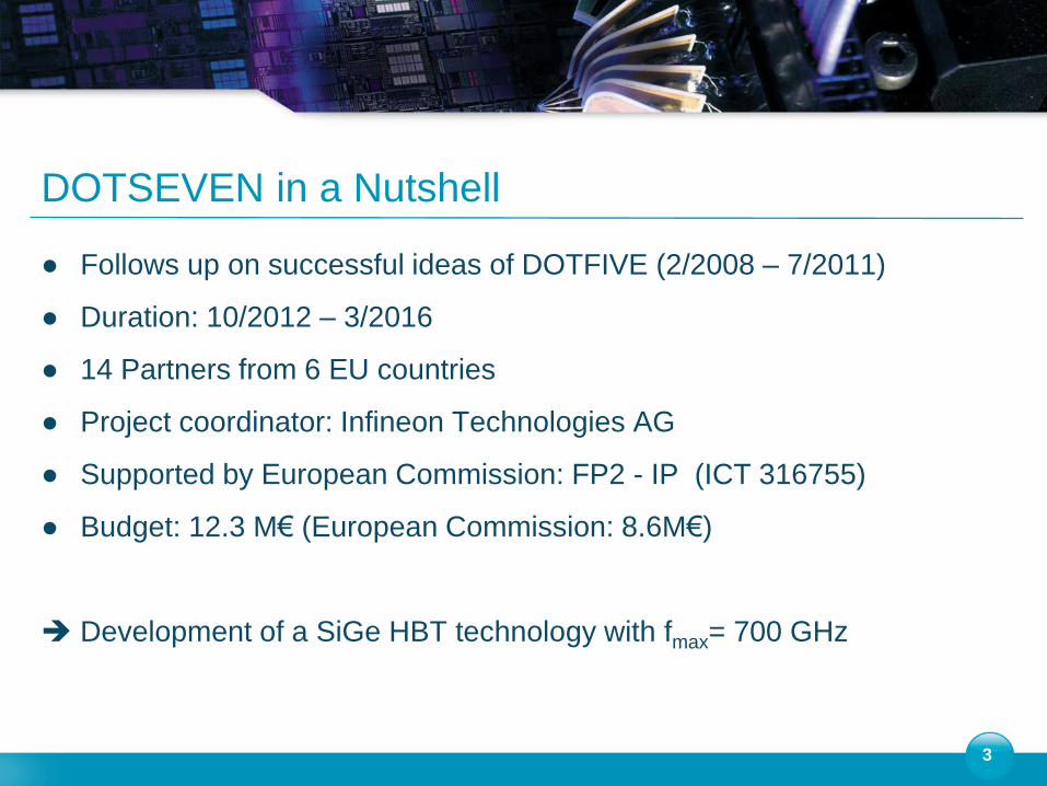
DOTSEVEN in a Nutshell
● Follows up on successful ideas of DOTFIVE (2/2008 – 7/2011)
● Duration: 10/2012 – 3/2016
● 14 Partners from 6 EU countries
● Project coordinator: Infineon Technologies AG
● Supported by European Commission: FP2 - IP (ICT 316755)
● Budget: 12.3 M€ (European Commission: 8.6M€)
Development of a SiGe HBT technology with fmax= 700 GHz
3
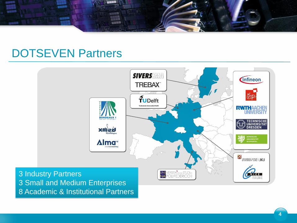
DOTSEVEN Partners
4
3 Industry Partners
3 Small and Medium Enterprises
8 Academic & Institutional Partners
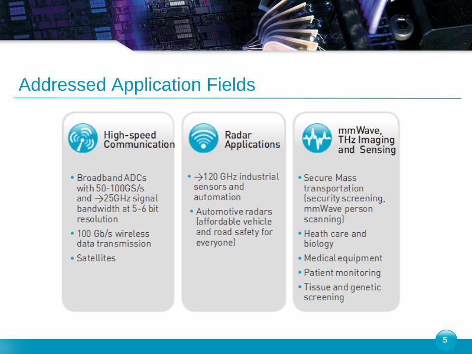
Addressed Application Fields
5
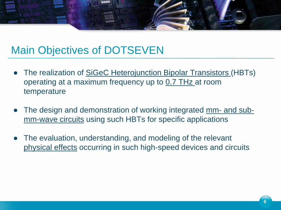
Main Objectives of DOTSEVEN
● The realization of SiGeC Heterojunction Bipolar Transistors (HBTs)
operating at a maximum frequency up to 0.7 THz at room
temperature
● The design and demonstration of working integrated mm- and sub-
mm-wave circuits using such HBTs for specific applications
● The evaluation, understanding, and modeling of the relevant
physical effects occurring in such high-speed devices and circuits
6
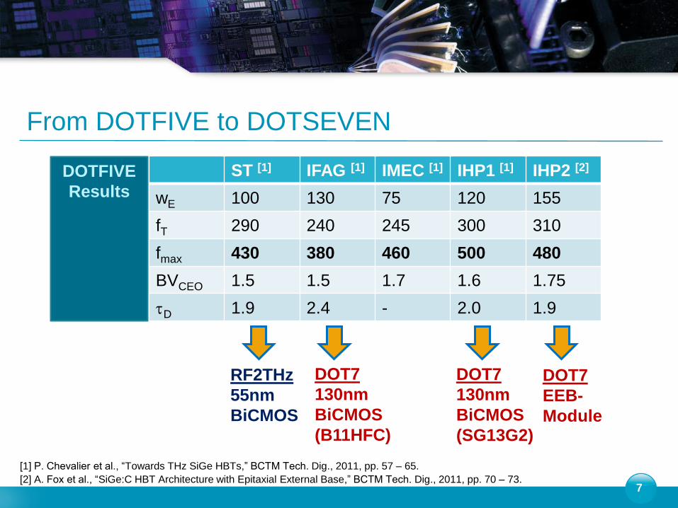
From DOTFIVE to DOTSEVEN
7
ST [1] IFAG [1] IMEC [1] IHP1 [1] IHP2 [2]
wE 100 130 75 120 155
fT 290 240 245 300 310
fmax 430 380 460 500 480
BVCEO 1.5 1.5 1.7 1.6 1.75
tD 1.9 2.4 - 2.0 1.9
[1] P. Chevalier et al., “Towards THz SiGe HBTs,” BCTM Tech. Dig., 2011, pp. 57 – 65.
[2] A. Fox et al., “SiGe:C HBT Architecture with Epitaxial External Base,” BCTM Tech. Dig., 2011, pp. 70 – 73.
DOTFIVE
Results
RF2THz
55nm
BiCMOS
DOT7
130nm
BiCMOS
(B11HFC)
DOT7
130nm
BiCMOS
(SG13G2)
DOT7
EEB-
Module
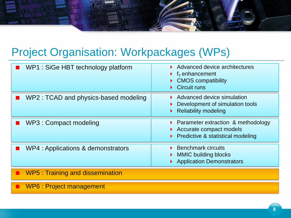
Project Organisation: Workpackages (WPs)
8
WP2 : TCAD and physics-based modeling
WP3 : Compact modeling
WP4 : Applications & demonstrators
Advanced device architectures
fT enhancement
CMOS compatibility
Circuit runs
WP1 : SiGe HBT technology platform
Advanced device simulation
Development of simulation tools
Reliability modeling
Parameter extraction & methodology
Accurate compact models
Predictive & statistical modeling
Benchmark circuits
MMIC building blocks
Application Demonstrators
WP5 : Training and dissemination
WP6 : Project management
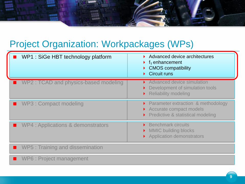
Project Organization: Workpackages (WPs)
9
WP2 : TCAD and physics-based modeling
WP3 : Compact modeling
WP4 : Applications & demonstrators
Advanced device architectures
fT enhancement
CMOS compatibility
Circuit runs
WP1 : SiGe HBT technology platform
Advanced device simulation
Development of simulation tools
Reliability modeling
Parameter extraction & methodology
Accurate compact models
Predictive & statistical modeling
Benchmark circuits
MMIC building blocks
Application demonstrators
WP5 : Training and dissemination
WP6 : Project management
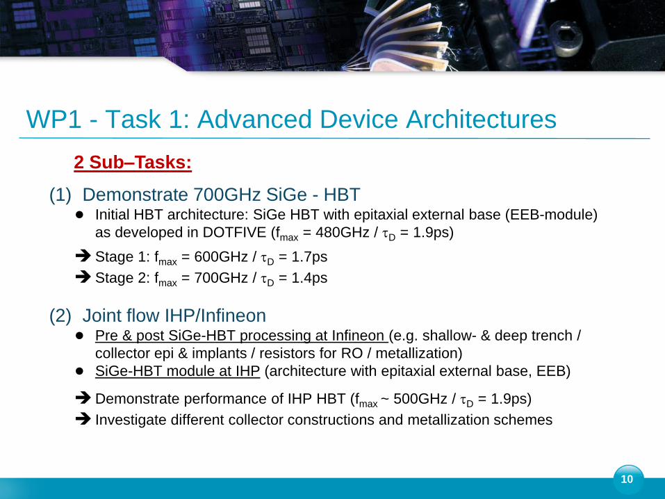
WP1 - Task 1: Advanced Device Architectures
(1) Demonstrate 700GHz SiGe - HBT ● Initial HBT architecture: SiGe HBT with epitaxial external base (EEB-module)
as developed in DOTFIVE (fmax = 480GHz / tD = 1.9ps)
Stage 1: fmax = 600GHz / tD = 1.7ps
Stage 2: fmax = 700GHz / tD = 1.4ps
(2) Joint flow IHP/Infineon ● Pre & post SiGe-HBT processing at Infineon (e.g. shallow- & deep trench /
collector epi & implants / resistors for RO / metallization)
● SiGe-HBT module at IHP (architecture with epitaxial external base, EEB)
Demonstrate performance of IHP HBT (fmax ~ 500GHz / tD = 1.9ps)
Investigate different collector constructions and metallization schemes
10
2 Sub–Tasks:
SIC SIC SIC SIC
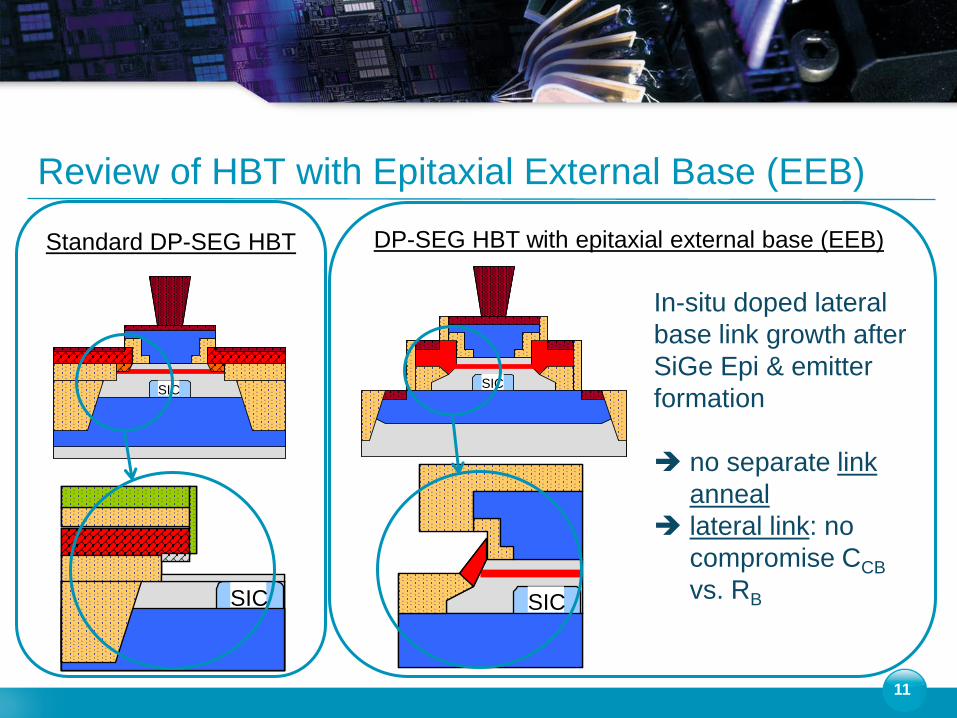
Review of HBT with Epitaxial External Base (EEB)
In-situ doped lateral
base link growth after
SiGe Epi & emitter
formation
no separate link
anneal
lateral link: no
compromise CCB
vs. RB
11
SIC SIC SIC SIC SIC
Standard DP-SEG HBT DP-SEG HBT with epitaxial external base (EEB)
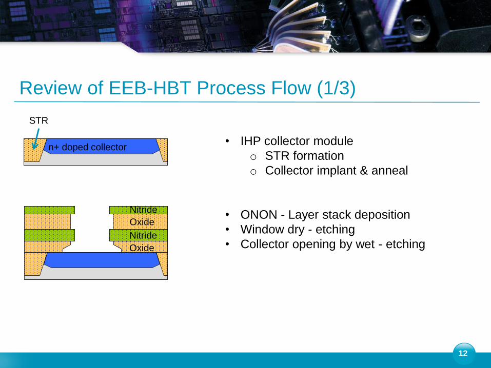
Review of EEB-HBT Process Flow (1/3)
12
n+ doped collector • IHP collector module
o STR formation
o Collector implant & anneal
• ONON - Layer stack deposition
• Window dry - etching
• Collector opening by wet - etching
STR
Oxide
Oxide
Nitride
Nitride
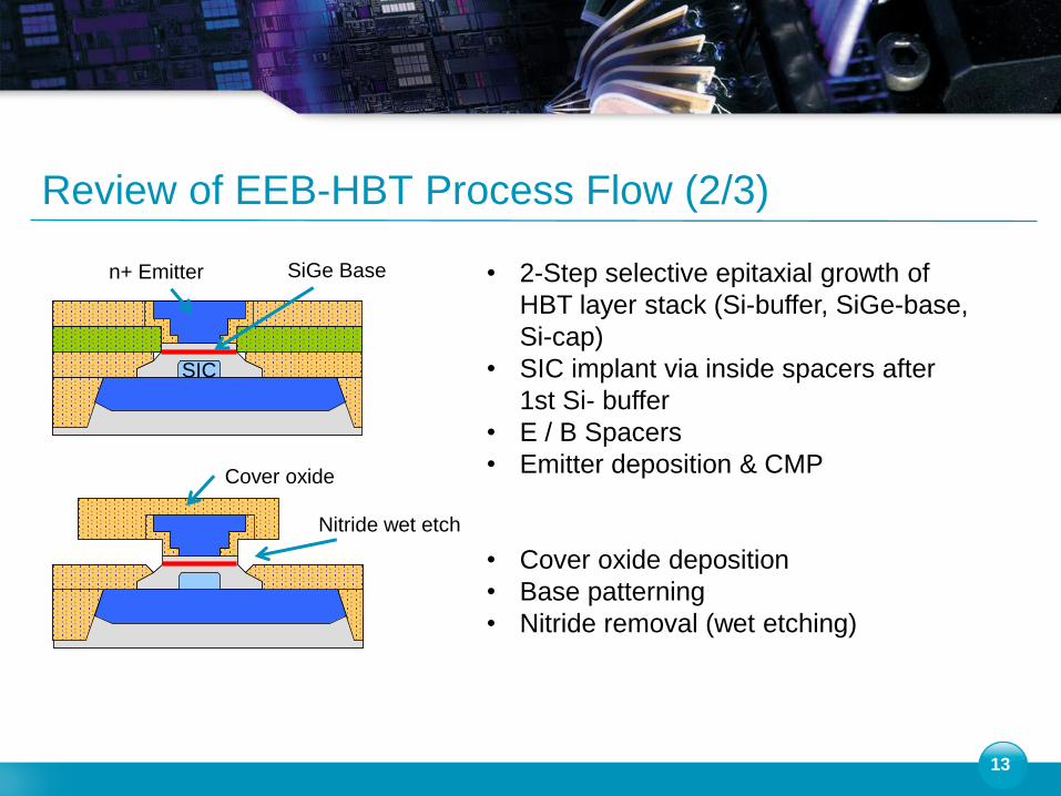
Review of EEB-HBT Process Flow (2/3)
13
• 2-Step selective epitaxial growth of
HBT layer stack (Si-buffer, SiGe-base,
Si-cap)
• SIC implant via inside spacers after
1st Si- buffer
• E / B Spacers
• Emitter deposition & CMP
• Cover oxide deposition
• Base patterning
• Nitride removal (wet etching)
SiGe Base
SIC
n+ Emitter
Cover oxide
Nitride wet etch
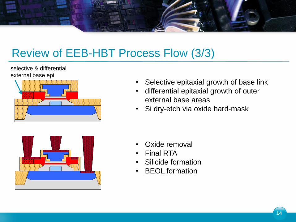
Review of EEB-HBT Process Flow (3/3)
14
• Selective epitaxial growth of base link
• differential epitaxial growth of outer
external base areas
• Si dry-etch via oxide hard-mask
• Oxide removal
• Final RTA
• Silicide formation
• BEOL formation
selective & differential
external base epi
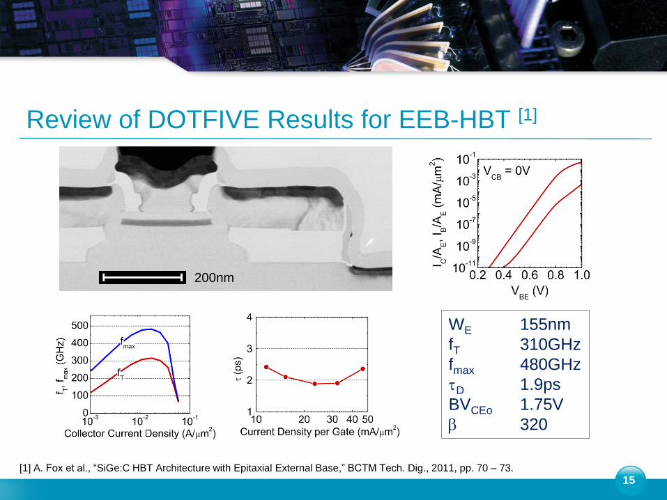
Review of DOTFIVE Results for EEB-HBT [1]
15
200nm200nm
[1] A. Fox et al., “SiGe:C HBT Architecture with Epitaxial External Base,” BCTM Tech. Dig., 2011, pp. 70 – 73.
WE 155nm
fT 310GHz
fmax 480GHz
tD 1.9ps
BVCEo 1.75V
b 320

Subtask 1: Planned EEB-HBT Process Development
16
● Lateral scaling of different dimensions (see next slide)
● Transfer layout from 0.25µm to 0.13µm design rules
● Process optimization of external base epitaxy
● Optimize process flow with respect to yield
This is expected to lead to the first stage of performance enhancement
The planning for the second stage will depend on results from this first
scaling stage and from results of WP1 - task 2 (vertical profile scaling)
and input from WP2 (device simulation) and WP3 (predictive modeling)
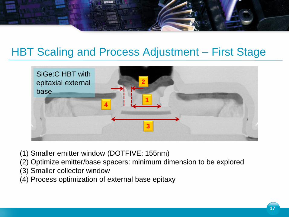
HBT Scaling and Process Adjustment – First Stage
17
2
1
3
4
(1) Smaller emitter window (DOTFIVE: 155nm)
(2) Optimize emitter/base spacers: minimum dimension to be explored
(3) Smaller collector window
(4) Process optimization of external base epitaxy
SiGe:C HBT with
epitaxial external
base
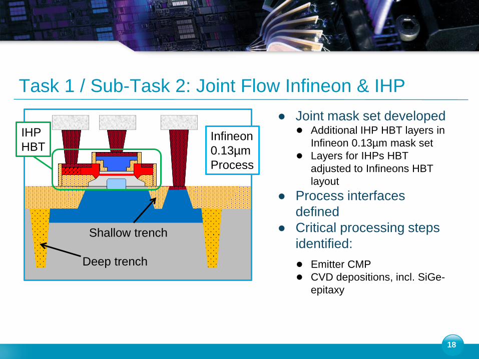
Task 1 / Sub-Task 2: Joint Flow Infineon & IHP
● Joint mask set developed ● Additional IHP HBT layers in
Infineon 0.13µm mask set
● Layers for IHPs HBT
adjusted to Infineons HBT
layout
● Process interfaces
defined
● Critical processing steps
identified:
● Emitter CMP
● CVD depositions, incl. SiGe-
epitaxy
18
Shallow trench
Deep trench
Infineon
0.13µm
Process
IHP
HBT
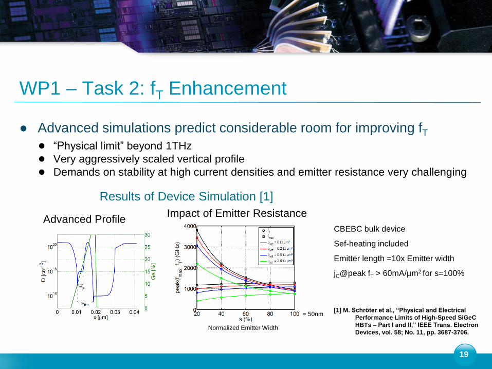
WP1 – Task 2: fT Enhancement
● Advanced simulations predict considerable room for improving fT
● “Physical limit” beyond 1THz
● Very aggressively scaled vertical profile
● Demands on stability at high current densities and emitter resistance very challenging
19
CBEBC bulk device
Sef-heating included
Emitter length =10x Emitter width
jC@peak fT > 60mA/µm2 for s=100%
Advanced Profile Impact of Emitter Resistance
Normalized Emitter Width
= 50nm
[1] M. Schröter et al., “Physical and Electrical
Performance Limits of High-Speed SiGeC
HBTs – Part I and II,” IEEE Trans. Electron
Devices, vol. 58; No. 11, pp. 3687-3706.
Results of Device Simulation [1]

Motivation for WP1 Task fT Enhancement
● Increase of high-speed circuit performance needs balanced
improvement of fmax and fT ● Appropriate ratio of fmax/fT needs to be clarified
● How realistic are the predictions?
● How far can fT be increased under manufacturability constraints?
20
Development of fT records for SiGe HBTs
Potential exhausted ?
FT
Fmax
BVCEO
Activities for WP1 Task fT Enhancement
● Develop flow with low-thermal budget for scaling of vertical profile
● Thermal treatments >650°C shall be avoided before final RTP step
● Optimize base profile on technology with non-selective base-epitaxy
● More flexibility for generating extreme profile variations
● Platform for device model parameter calibration
● Fabrication of HBTs with special base profiles for validating device simulations
● Impact of back-end processes have to be investigated
● First studies for fT maximization don’t need further lateral scaling
● Only in 2nd project phase test of optimized vertical profiles in flows with low external
parasitics
21
WP1 – Task 3: CMOS Compatibility
● DOTFIVE: pure bipolar technology developed
● Suitable for applications like 60GHz WLAN or 77GHz radar
● Future product generations require more digital functionality
● E.g. memory, interfaces, A/D conversion and base band processing
BiCMOS integration will be investigated in DOTSEVEN
● Integration of the conventional (DPSA-) SiGe HBT developed in DOTFIVE into a
130nm CMOS platform at Infineon
● Investigation of possibility to adapt IHP’s HBT with epitaxially grown base link to
Infineon’s 130nm BiCMOS platform
● IHP SG13G2
22
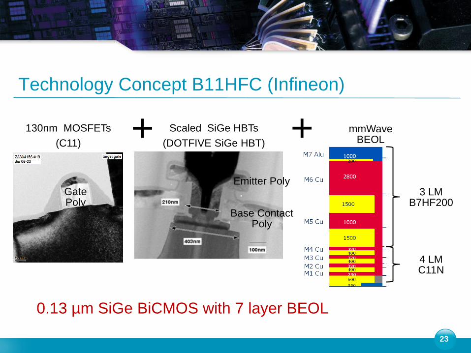
Technology Concept B11HFC (Infineon)
23
130nm MOSFETs
(C11)
Gate Poly
Scaled SiGe HBTs
(DOTFIVE SiGe HBT)
Base Contact Poly
Emitter Poly
4 LM C11N
3 LM B7HF200
mmWave BEOL + +
0.13 µm SiGe BiCMOS with 7 layer BEOL

Constrains of HBT Integration into CMOS
● General constraint for BiCMOS development in practice:
● HBT is integrated into an established CMOS technology
CMOS devices should not be changed (reuse CMOS IP, ROM, SRAM, …)
● MOS thermal steps (LDD-, SD-anneals, poly oxidation) deteriorate HBT performance
● Three problems were identified for integration of DOTFIVE HBT into
Infineon‘s 130nm CMOS technology
(1) Wafer orientation for best HBT performance and yield (notch in [010] orientation) is
different from CMOS standard
(2) Incompatible thermal budgets for HBT and CMOS fabrication
(3) Structural problems during process integration
24
CMOS Integration Problems: Corrective Measures
● (1) Substrate orientation: adjust CMOS
● Re-center MOS parameters by modification of implant and anneal steps
● (2) Thermal budget: find compromise
● Reduce LDD anneal so that the MOS-parameters can still be re-centered and the base
can be deposited before CMOS spacers
● Reduce S/D anneal so that MOS parameters can still be re-centered
● Adjust base- and emitter-modules of the HBT to the reduced S/D anneal (which is still
higher than in the DOTFIVE HBT process)
● (3) Structural problems: manifold!
● Example: removal of layers of bipolar fabrication from MOS-gates introduction of a
nitride protection layer that acts as etch-stop-layer during layer removal
25
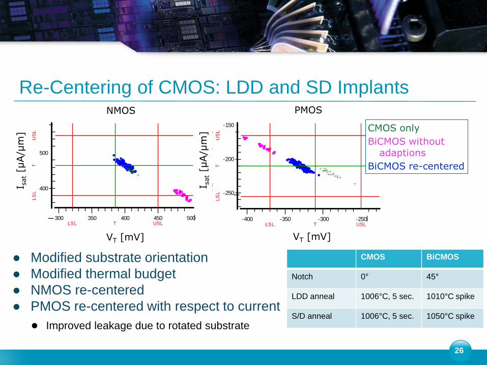
Re-Centering of CMOS: LDD and SD Implants
● Modified substrate orientation
● Modified thermal budget
● NMOS re-centered
● PMOS re-centered with respect to current
● Improved leakage due to rotated substrate
26
300 350 400 450 500
VTSnr_10x012;mean [mV]
400
500
IDS
nr_
10x012;m
ean [uA
/um
]
LSL USLT
LS
LU
SL
T LEGEND
group
BiCMOS
BiCMOS emulation
CMOS
CorrelationPlot VTSnr_10x012;mean - IDSnr_10x012;mean grouped by group
X: lo 320 hi 450 qty 171/171 mean 411.5 sigma 27.29 cp 0.794 cpk 0.471
Y: lo 380 hi 550 qty 171/171 mean 453.8 sigma 26.83 cp 1.06 cpk 0.916NMOS
VT [mV]
I sat [µ
A/µ
m]
-400 -350 -300 -250
VTSpr_10x012;mean [mV]
-250
-200
-150
IDS
pr_
10x012;m
ean [uA
/um
]
LSL USLT
LS
LU
SL
T LEGEND
group
BiCMOS
BiCMOS emulation
CMOS
CorrelationPlot VTSpr_10x012;mean - IDSpr_10x012;mean grouped by group
X: lo -370 hi -250 qty 171/171 mean -330.2 sigma 22.75 cp 0.879 cpk 0.583
Y: lo -255 hi -165 qty 171/171 mean -208.9 sigma 11.35 cp 1.32 cpk 1.29PMOS
VT [mV]
I sat [µ
A/µ
m] CMOS only
BiCMOS without adaptions
BiCMOS re-centered
CMOS BiCMOS
Notch 0° 45°
LDD anneal 1006°C, 5 sec. 1010°C spike
S/D anneal 1006°C, 5 sec. 1050°C spike
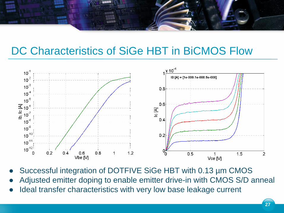
DC Characteristics of SiGe HBT in BiCMOS Flow
● Successful integration of DOTFIVE SiGe HBT with 0.13 µm CMOS
● Adjusted emitter doping to enable emitter drive-in with CMOS S/D anneal
● Ideal transfer characteristics with very low base leakage current
27
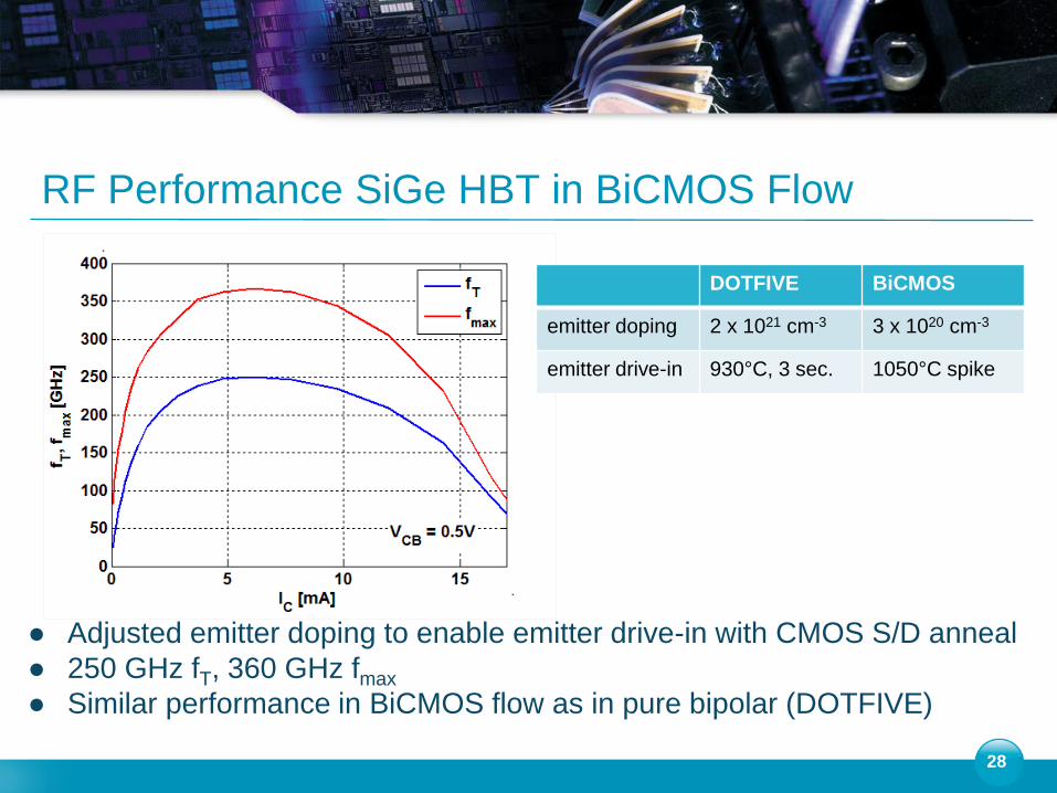
RF Performance SiGe HBT in BiCMOS Flow
● Adjusted emitter doping to enable emitter drive-in with CMOS S/D anneal
● 250 GHz fT, 360 GHz fmax
● Similar performance in BiCMOS flow as in pure bipolar (DOTFIVE)
28
DOTFIVE BiCMOS
emitter doping 2 x 1021 cm-3 3 x 1020 cm-3
emitter drive-in 930°C, 3 sec. 1050°C spike
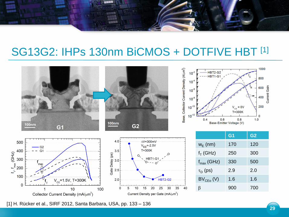
SG13G2: IHPs 130nm BiCMOS + DOTFIVE HBT [1]
29 [1] H. Rücker et al., SIRF 2012, Santa Barbara, USA, pp. 133 – 136
G1 G2
wE (nm) 170 120
fT (GHz) 250 300
fmax (GHz) 330 500
tD (ps) 2.9 2.0
BVCEo (V) 1.6 1.6
b 900 700
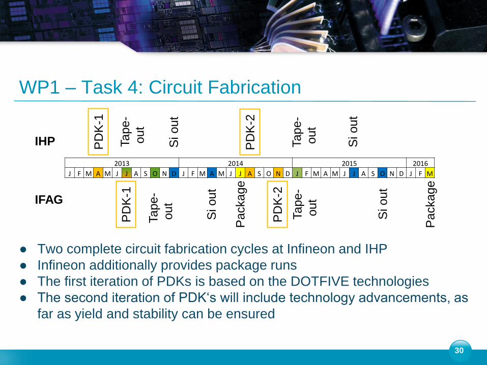
WP1 – Task 4: Circuit Fabrication
● Two complete circuit fabrication cycles at Infineon and IHP
● Infineon additionally provides package runs
● The first iteration of PDKs is based on the DOTFIVE technologies
● The second iteration of PDK‘s will include technology advancements, as
far as yield and stability can be ensured
30
IHP
IFAG
PD
K-1
Tape-
out
Si out
PD
K-2
Tape-
out
Si out
PD
K-1
Tape-
out
Si out
PD
K-2
Tape-
out
Si out
2013 2014 2015 2016
J F M A M J J A S O N D J F M A M J J A S O N D J F M A M J J A S O N D J F M
Package
Package
Infineon Process Design Kit for First Design Cycle
31
● Process B11HFC: 130nm BiCMOS process with latest DOTFIVE HBT
performance level
● PDK including the required simulation models, layout cells, and
verification tools (DRC, LVS, …) delivered to the circuit partners
● Comprehensive library of scalable npn transistors for optimizing
applications (emitter length range of 0.7µm to 10.0µm, different contact
configurations like BEC, BEBC, CBEBC, …)
● TaN resistor, MIM capacitor, high-performance varactor (based on the
high voltage npn transistor), transmission lines, …
● Physics-based compact models, including advanced HiCUM models for
the high speed npn transistors by TU Dresden
Infineon Process Design Kit for First Design Cycle
32
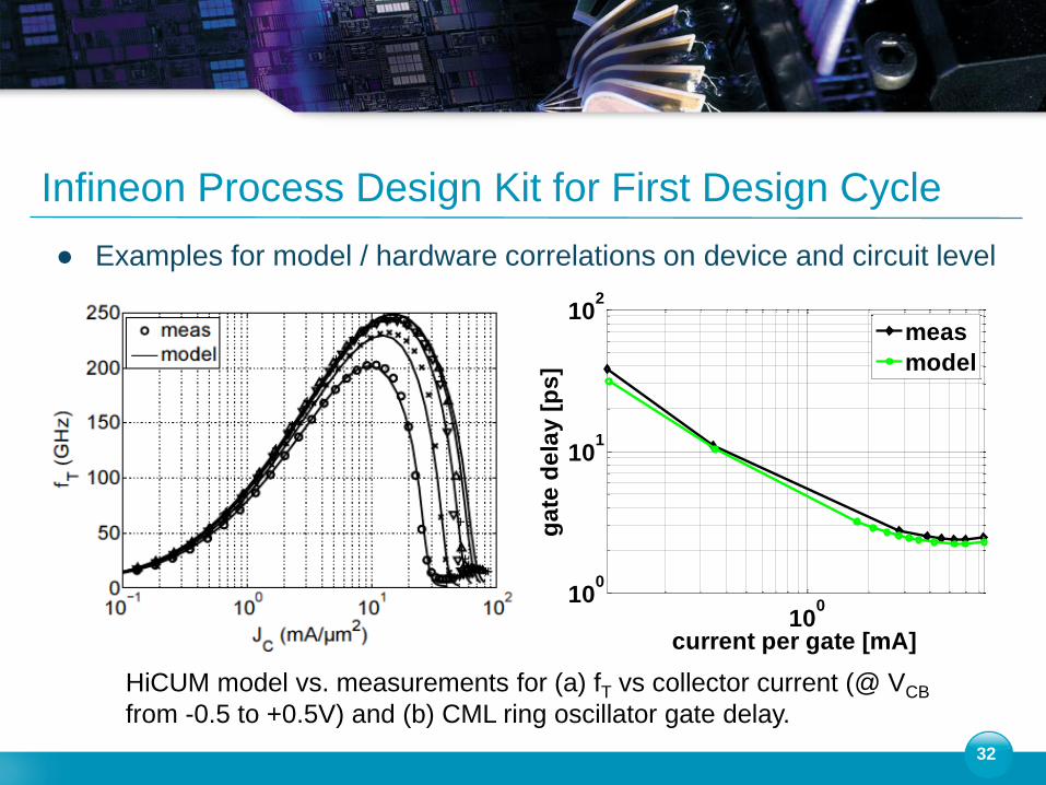
● Examples for model / hardware correlations on device and circuit level
HiCUM model vs. measurements for (a) fT vs collector current (@ VCB
from -0.5 to +0.5V) and (b) CML ring oscillator gate delay.
100
100
101
102
current per gate [mA]
ga
te d
ela
y [
ps
]
meas
model
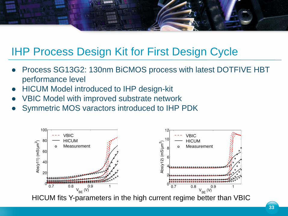
IHP Process Design Kit for First Design Cycle
● Process SG13G2: 130nm BiCMOS process with latest DOTFIVE HBT
performance level
● HICUM Model introduced to IHP design-kit
● VBIC Model with improved substrate network
● Symmetric MOS varactors introduced to IHP PDK
33
°
VBIC
HICUM
Measurement °
VBIC
HICUM
Measurement
HICUM fits Y-parameters in the high current regime better than VBIC
Summary
● HBTs with fmax = 700GHz / tD = 1.4ps and circuit demonstrators
operating up to 240GHz are targeted for Q1 2016
● In the first step improvements up to fmax = 600GHz/tD = 1.7ps are
expected by scaling the HBT architecture with epitaxial external base
(EEB) developed in DOTFIVE
● Industry compatibility of the EEB architecture will be tested in a joint flow
between Infineon and IHP
● fT limits will be explored by testing aggressive vertical profiles
● Investigate BiCMOS integration issues of advanced SiGe HBTs
● Two complete design cycles by both technology partners are scheduled
for demonstration of integrated mm- and sub-mm-wave circuits
34
Acknowledgement
● Andreas Pawlack, Julia Krause (TU Dresden, HiCUM modelling)
● Holger Rücker (IHP)
35


![SiGe BiCMOS for Analog, High-Speed Digital and Millimetre ...tcc/bctm_06_sv.pdf · BiCMOS process development [1]-[3]. While SiGe HBT performance has steadily improved over the last](https://static.fdocuments.in/doc/165x107/5ea16431fda46c45b810fb45/sige-bicmos-for-analog-high-speed-digital-and-millimetre-tccbctm06svpdf.jpg)