EE241 - Spring 2013bwrcs.eecs.berkeley.edu/Classes/icdesign/ee241_s13/... · EE241 - Spring 2013...
19
1 EE241 - Spring 2013 Advanced Digital Integrated Circuits Lecture 8: Variability SRAM Design 2 Announcements Homework 1 due today Homework 2 posted this week
Transcript of EE241 - Spring 2013bwrcs.eecs.berkeley.edu/Classes/icdesign/ee241_s13/... · EE241 - Spring 2013...

1
EE241 - Spring 2013Advanced Digital Integrated Circuits
Lecture 8: VariabilitySRAM Design
2
Announcements
Homework 1 due today
Homework 2 posted this week
2
3
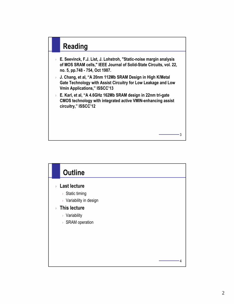
Reading
E. Seevinck, F.J. List, J. Lohstroh, "Static-noise margin analysis of MOS SRAM cells," IEEE Journal of Solid-State Circuits, vol. 22, no. 5, pp.748 - 754, Oct 1987.
J. Chang, et al, “A 20nm 112Mb SRAM Design in High K/Metal Gate Technology with Assist Circuitry for Low Leakage and Low Vmin Applications,” ISSCC’13
E. Karl, et al, “A 4.6GHz 162Mb SRAM design in 22nm tri-gate CMOS technology with integrated active VMIN-enhancing assist circuitry,” ISSCC’12
4
Outline
Last lectureStatic timing
Variability in design
This lectureVariability
SRAM operation
3
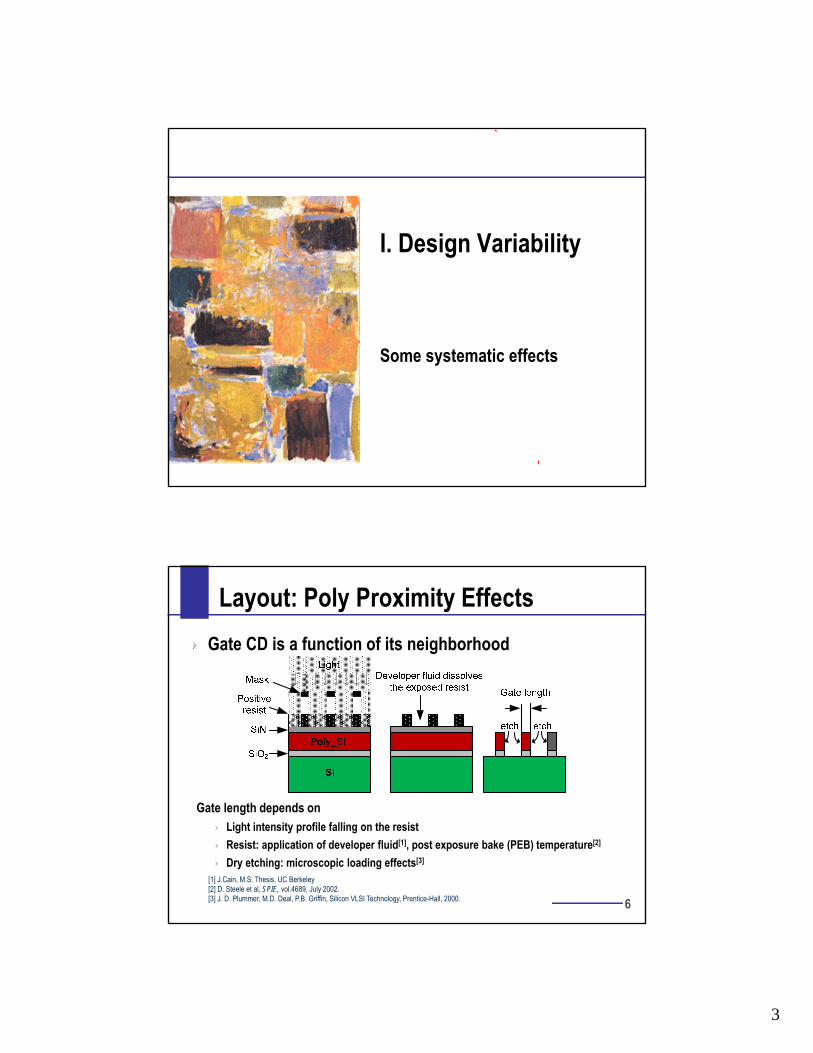
I. Design Variability
Some systematic effects
6
Layout: Poly Proximity Effects
Gate CD is a function of its neighborhood
Gate length depends onLight intensity profile falling on the resist
Resist: application of developer fluid[1], post exposure bake (PEB) temperature[2]
Dry etching: microscopic loading effects[3]
[1] J.Cain, M.S. Thesis, UC Berkeley[2] D. Steele et al, SPIE, vol.4689, July 2002.[3] J. D. Plummer, M.D. Deal, P.B. Griffin, Silicon VLSI Technology, Prentice-Hall, 2000.
4
7
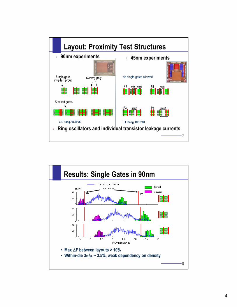
Layout: Proximity Test Structures
min max2P1 mid1P2
max1P3 max2P4
90nm experiments 45nm experiments
L.T. Pang, VLSI’06 L.T. Pang, CICC’08
No single gates allowed
Ring oscillators and individual transistor leakage currents
8
Results: Single Gates in 90nm
• Max F between layouts > 10%• Within-die 3/ ~ 3.5%, weak dependency on density
5
9
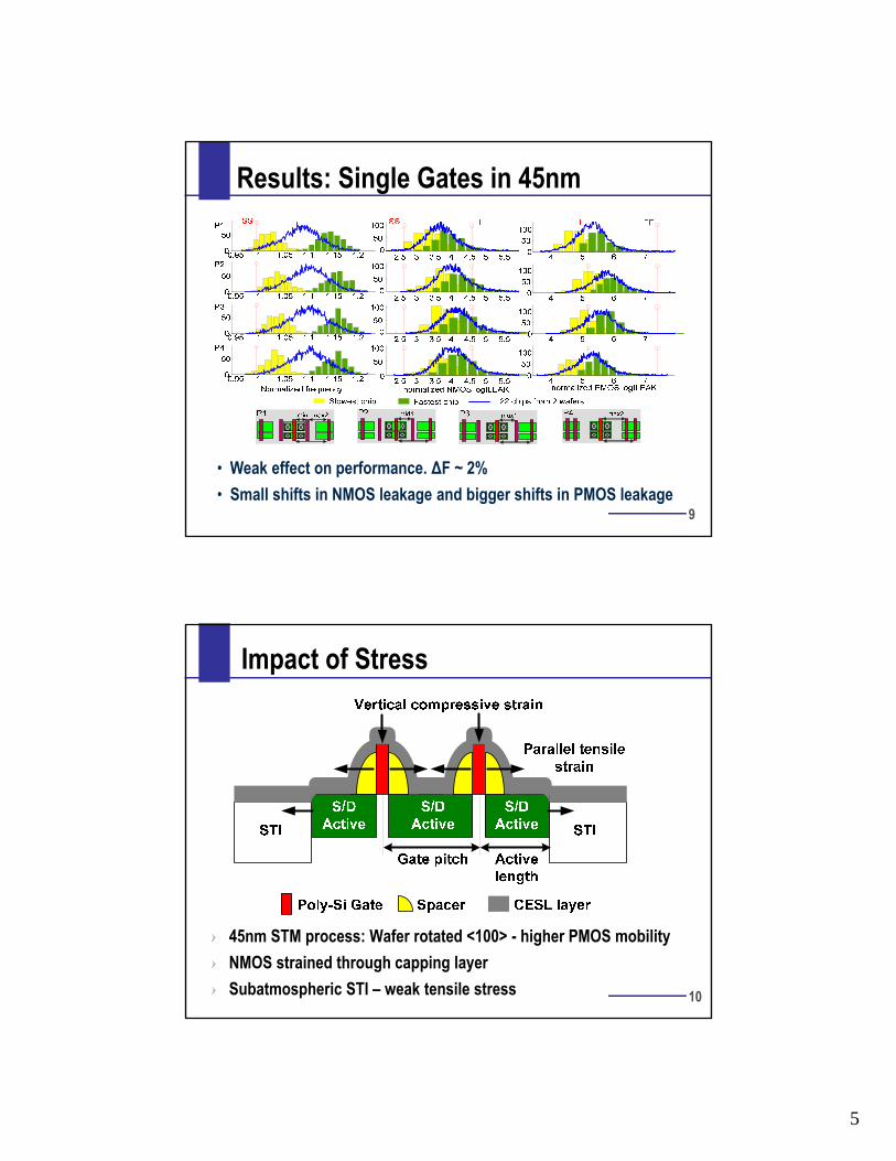
Results: Single Gates in 45nm
• Weak effect on performance. ΔF ~ 2%
• Small shifts in NMOS leakage and bigger shifts in PMOS leakage
10
Impact of Stress
45nm STM process: Wafer rotated <100> - higher PMOS mobility
NMOS strained through capping layer
Subatmospheric STI – weak tensile stress

6
11
Impact of Longer Diffusion in 45nm
• Strongest effect measured in 45nm, ΔF ~ 5%
• No significant shift in ILEAK
Fastest chipSlowest chip
22 chips from 2 wafers
max1
Longer diffusion
D1max1P3
4 5 6 7Norm. PMOS logILEAK
TT FF
0.95 1 1.05 1.1 1.15 1.2 1.25Norm. frequency
40
80
40
80
SS
0
0
D1
P3 TT
3 4 5 6Norm. NMOS logILEAK
SS TT
50
100
50
100
0
0
RO Frequency NMOS ILEAK PMOS ILEAK
12
Impact of Shallow Trench Isolation (STI)
• ΔF ~ 3%, small changes in ILEAK
• Due to STI-induced stress
Fastest chip
Slowest chip
22 chips from 2 wafers
min
R1
min
NSTI
40
80
1 1.05 1.1 1.15 1.2
40
80
Norm. frequency0.95
SS
0
0
R1
NSTI
4 5 6 7Norm. PMOS logILEAK
TT
2 3 4 5Norm. NMOS logILEAK
50
100
50
100
SS TT
0
0
RO Frequency NMOS ILEAK PMOS ILEAK

7
13
Chip Yield Depends on Inter-Gate Correlation
d1 d2 dn
n stages
D D
Yield = Pr (sum of n delays < clock period)
= 0 gives highest yield through averaging
Variation remains constant with correlated gates, = 1
1 / sqrt(n)
0%
5%
10%
15%
20%
0 2 4 6 8 10
Number of stages (n)
/m
ean
of to
tal d
elay Variation is reduced with
non-correlated gates, = 0
Non-correlated gates in a path reduce impact of variation
Bowman et al, JSSC, Feb 2002 .
14
Chip Yield Depends on Inter-Path Correlation
Bowman et al, JSSC, Feb 2002 .
K u
ncor
rela
ted
path
s
Yield = Pr (max delay of K paths < clock period)
K = 1 gives highest yield
Normalized Critical Path DelayMax delay of P paths
Nor
mal
ized
PD
F
0.8 0.9 1 1.1 1.20
Mean delay increases as K increases for uncorrelated paths
K =1K =2K =10000
aP bP cPD D
a1 b2 c1D D
Correlated paths reduce impact of variation
8
J. Design Variability
Some random effects
16
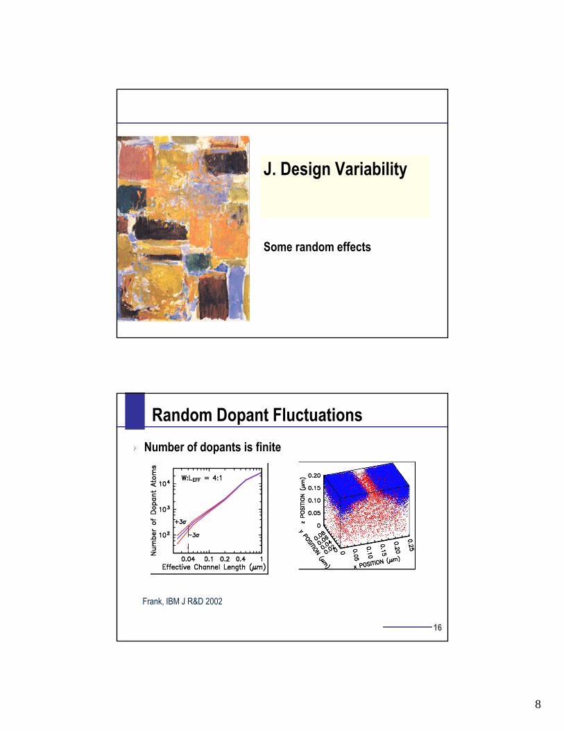
Random Dopant Fluctuations
Number of dopants is finite
Frank, IBM J R&D 2002

9
17
Random Dopant Fluctuations
Lg = 17nm, VDS = 0.7V Lg = 11nm, VDS = 0.7V
VT = 23mV VT = 52mV
18
Processing: Line-Edge Roughness
•Sources of line-edge roughness:• Fluctuations in the total dose due to quantization• Resist composition• Absorption positionsEffect:• Variation (random) in leakage and power

10
19
Oxide Thickness
Systematic variations +
Roughness in the Si./SiO2 interface
Smaller effect than RDF
Asenov, TED’2002
20
Transistor Matching
Transistor VThs vary with size (~ ) and distance
Pelgrom parameter AVT
- Scales with technology (EOT)
J. Mazurier, Trans E.D., 2011.
AVT in FDSOI technology
11
21
Negative Bias Temperature Instability
PFET VTh’s shift in time, at high negative bias and elevated temperatures
The mechanism is thought to be the breaking of hydrogen-silicon bonds at the Si/SiO2 interface, creating surface traps and injecting positive hydrogen-related species into the oxide.
Also other charge trapping and hot-carrier defect generation
Systematic + random shifts
Tsujikawa, IRPS’2003
22
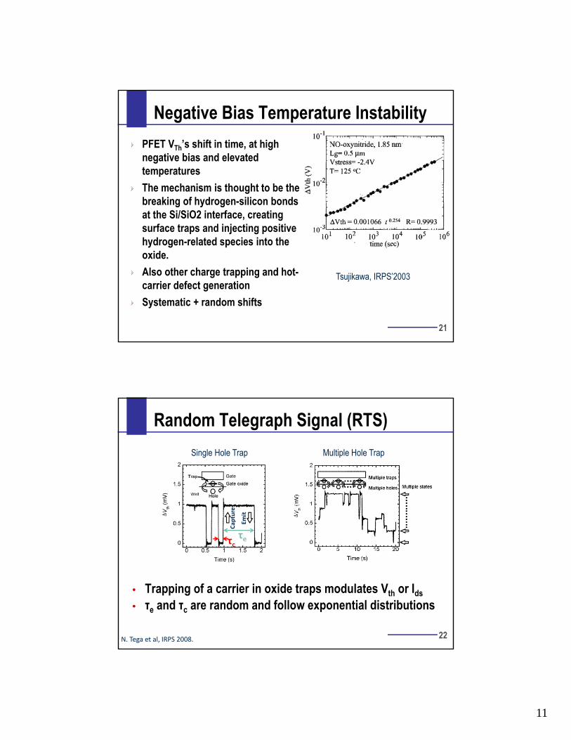
Random Telegraph Signal (RTS)
• Trapping of a carrier in oxide traps modulates Vth or Ids
• τe and τc are random and follow exponential distributions
Single Hole Trap Multiple Hole Trap
N. Tega et al, IRPS 2008.
τcτe
Cap
ture
Emit

12
23
-4
-3
-2
-1
0
1
2
3
4
1 10 100C
DF
(σ
)∆Vth (mV)
RTS
RDF
RTS and Technology Scaling
RTS exceeds RDF at 3 sigma in the 22nm node
Tega et. al, VLSI Tech. 09
L/W = 20/45nm
WL1
ΔVth, RTS~
WL
1ΔVth, RDF
~
SRAM
Read/Write/Retention Margins
13
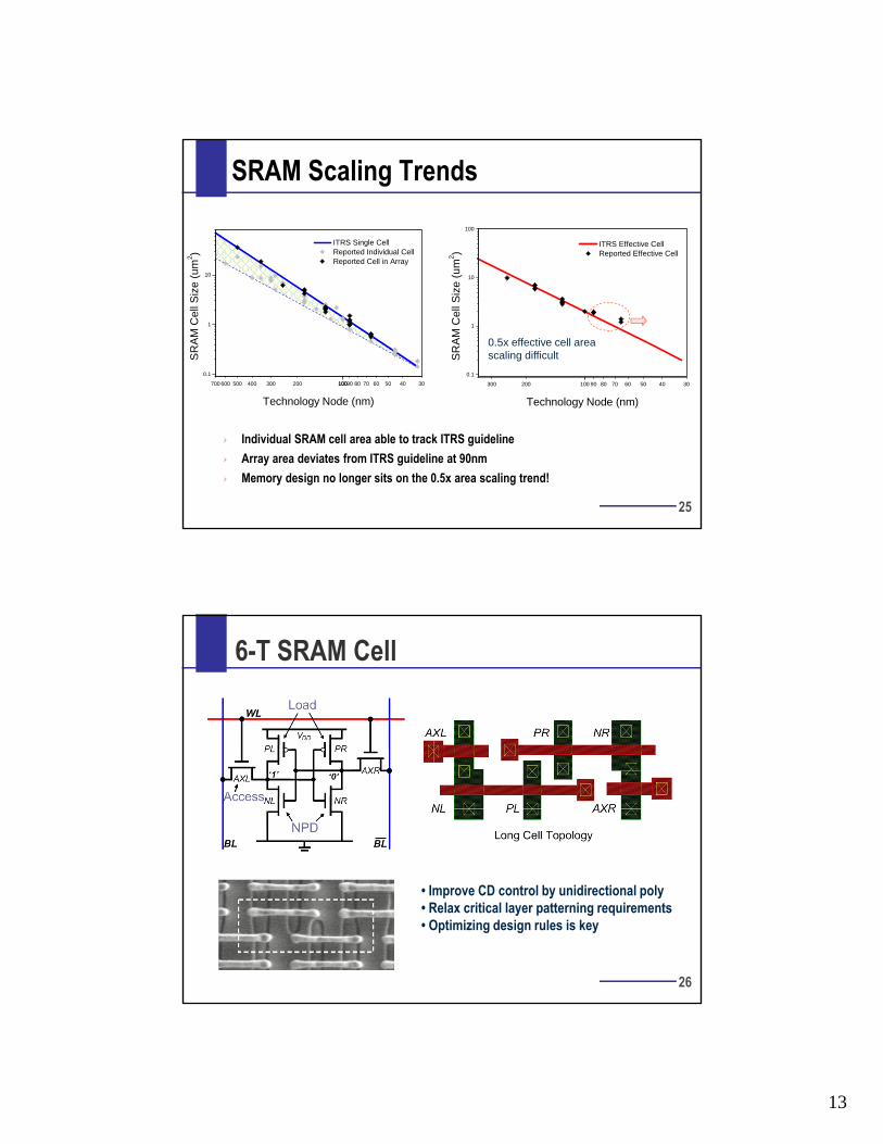
25
700 600 500 400 300 200 10010090 80 70 60 50 40 30
0.1
1
10
ITRS Single Cell Reported Individual Cell Reported Cell in Array
SR
AM
Cel
l Siz
e (u
m2 )
Technology Node (nm)
SRAM Scaling Trends
Individual SRAM cell area able to track ITRS guideline
Array area deviates from ITRS guideline at 90nm
Memory design no longer sits on the 0.5x area scaling trend!
300 200 100 90 80 70 60 50 40 30
0.1
1
10
100
ITRS Effective Cell Reported Effective Cell
SR
AM
Cel
l Siz
e (
um
2)
Technology Node (nm)
0.5x effective cell area scaling difficult
26
6-T SRAM Cell
• Improve CD control by unidirectional poly• Relax critical layer patterning requirements• Optimizing design rules is key

14
27
SRAM Cell Design Trends
• Key enabling technology
• Impact:
Cell in 90nm(1m2)
Cell in 32nm(0.171m2)
IEDM
’
02
VDD
GND
WL
BL BLB
28
More SRAM Trends
0.15m2 cell in 32nm from TSMC (IEDM’07)
0.1m2 cell in 22nm from IBM (IEDM’08)
15
29
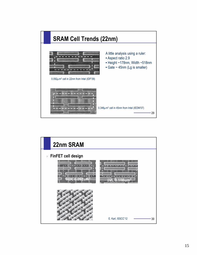
SRAM Cell Trends (22nm)
0.092m2 cell in 22nm from Intel (IDF’09)
0.346m2 cell in 45nm from Intel (IEDM’07)
A little analysis using a ruler:• Aspect ratio 2.9• Height ~178nm, Width ~518nm• Gate ~ 45nm (Lg is smaller)
30
22nm SRAM
FinFET cell design
E. Karl, ISSCC’12
16
SRAM
Static Retention Margin
32
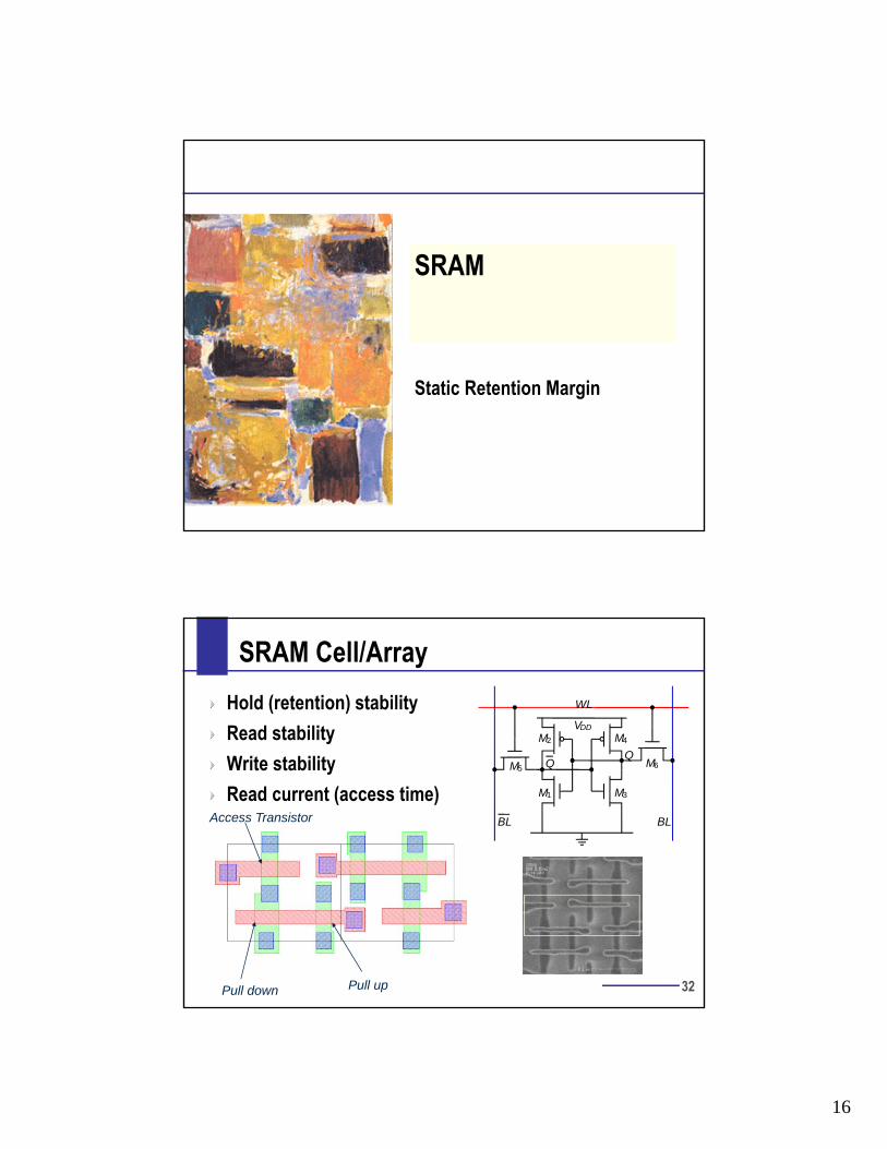
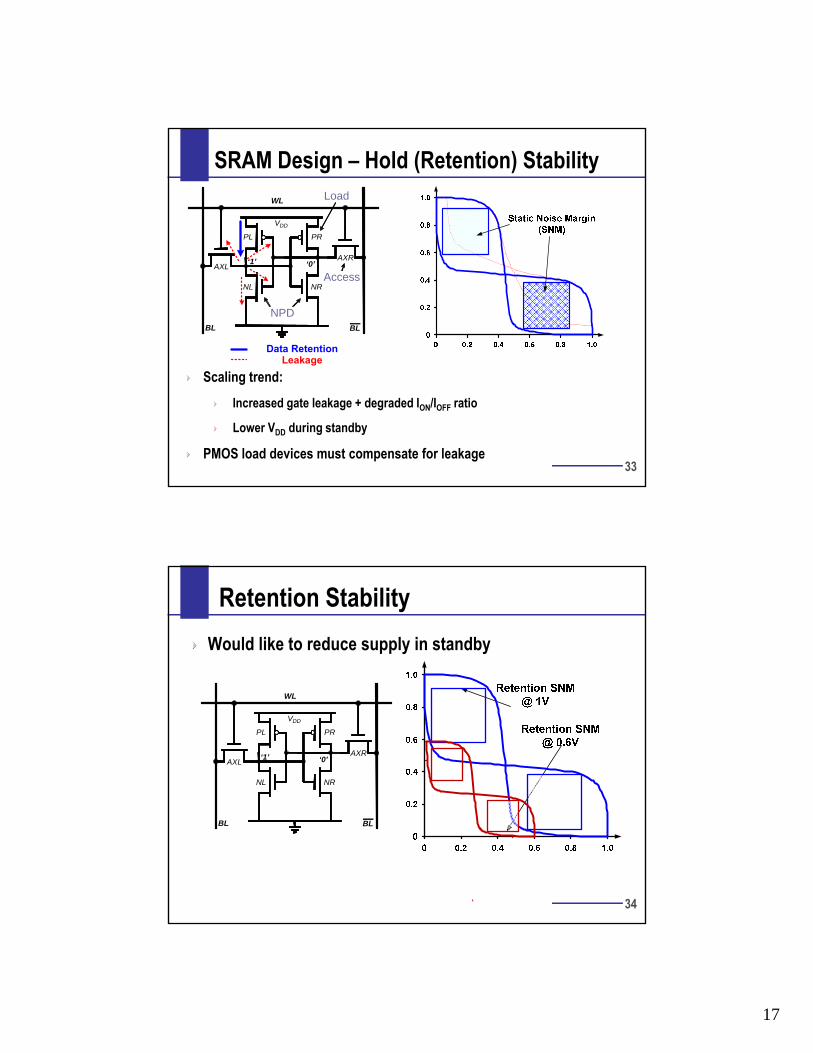
SRAM Cell/Array
Hold (retention) stability
Read stability
Write stability
Read current (access time)
WL
BL
VDD
M5 M6
M4
M1
M2
M3
BL
Access Transistor
Pull down Pull up
17
33
WL
BL
AXL
NPD
Access
‘1’ ‘0’
Load
AXR
NRNL
PRPL
BL
VDD
Data RetentionLeakage
Scaling trend:
Increased gate leakage + degraded ION/IOFF ratio
Lower VDD during standby
PMOS load devices must compensate for leakage
SRAM Design – Hold (Retention) Stability
34
Retention Stability
Would like to reduce supply in standby
WL
BL
AXL‘1’ ‘0’
AXR
NRNL
PRPL
BL
VDD
18
350 50 100 150 200 250 300
0
50
100
150
200
250
300
Simulated DRV of 1500 SRAM cells (mV)
His
togr
am o
f cel
l #
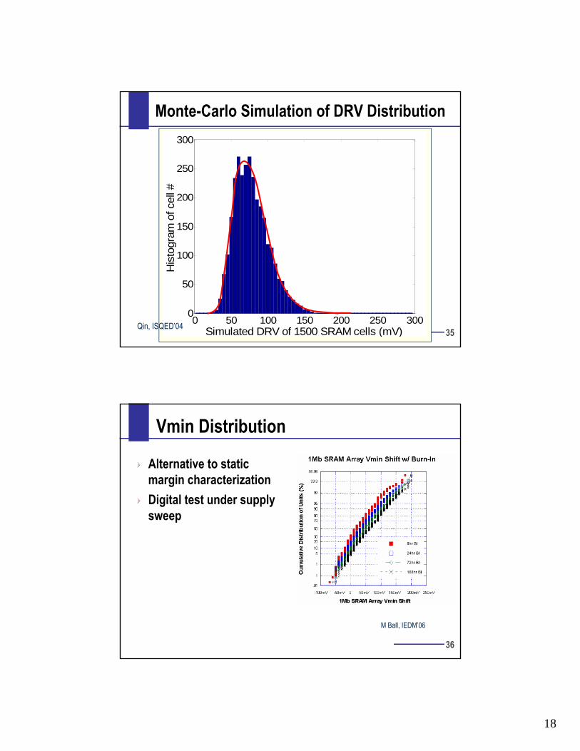
Monte-Carlo Simulation of DRV Distribution
Qin, ISQED’04
36
Vmin Distribution
Alternative to static margin characterization
Digital test under supply sweep
M Ball, IEDM’06

19
37
Next Lecture
SRAM as an example of variability-aware design


![Analysis of 6T FinFET SRAM Assist Techniques and …djseo/classes/ee241/...EE241 Final Report 2 (a) (b) (c) Fig. 1 FinFET-based SRAM cell array published by [1]. High Density Cell](https://static.fdocuments.in/doc/165x107/5ae6f2697f8b9a6d4f8d666f/analysis-of-6t-finfet-sram-assist-techniques-and-djseoclassesee241ee241.jpg)