
EE241 - Spring 2005 - University of California,...
26
1 EE241 - Spring 2005 Advanced Digital Integrated Circuits Lecture 10: Power Intro 2 Admin Project Phase 2 due Monday March 14, 5pm (by e-mail to [email protected] and [email protected]) Should be a 3 page (max) double-column conference style paper (submitted in word or pdf). No fonts smaller than 10 point. Should describe motivation and goals of your project, describe what you have learned so far from studying the background material and by your own analysis, and spell out what you expect to do by the end of the semester – That is, how will you evaluate and/or demonstrate your results. Two lectures on We afternoon (2pm and 3:30pm). No lecture next Monday.
Transcript of EE241 - Spring 2005 - University of California,...

1
EE241 - Spring 2005Advanced Digital Integrated Circuits
Lecture 10:Power Intro
2
Admin
Project Phase 2 due Monday March 14, 5pm (by e-mail to [email protected] and [email protected])
Should be a 3 page (max) double-column conference style paper (submitted in word or pdf). No fonts smaller than 10 point.
Should describe motivation and goals of your project, describe what you have learned so far from studying the background material and by your own analysis, and spell out what you expectto do by the end of the semester – That is, how will you evaluate and/or demonstrate your results.
Two lectures on We afternoon (2pm and 3:30pm). No lecture next Monday.

2
3
Wrapping up HS: Other Logic Styles
Dominant logic styles: static, PTL, Dynamic
Search for other options is continuously going on (noise margins, leakage, higher performance)
The balance is shifting with every new technology generation
4
Sense-Amplifying Logic
Matsui,JSSC 12/94
3
5
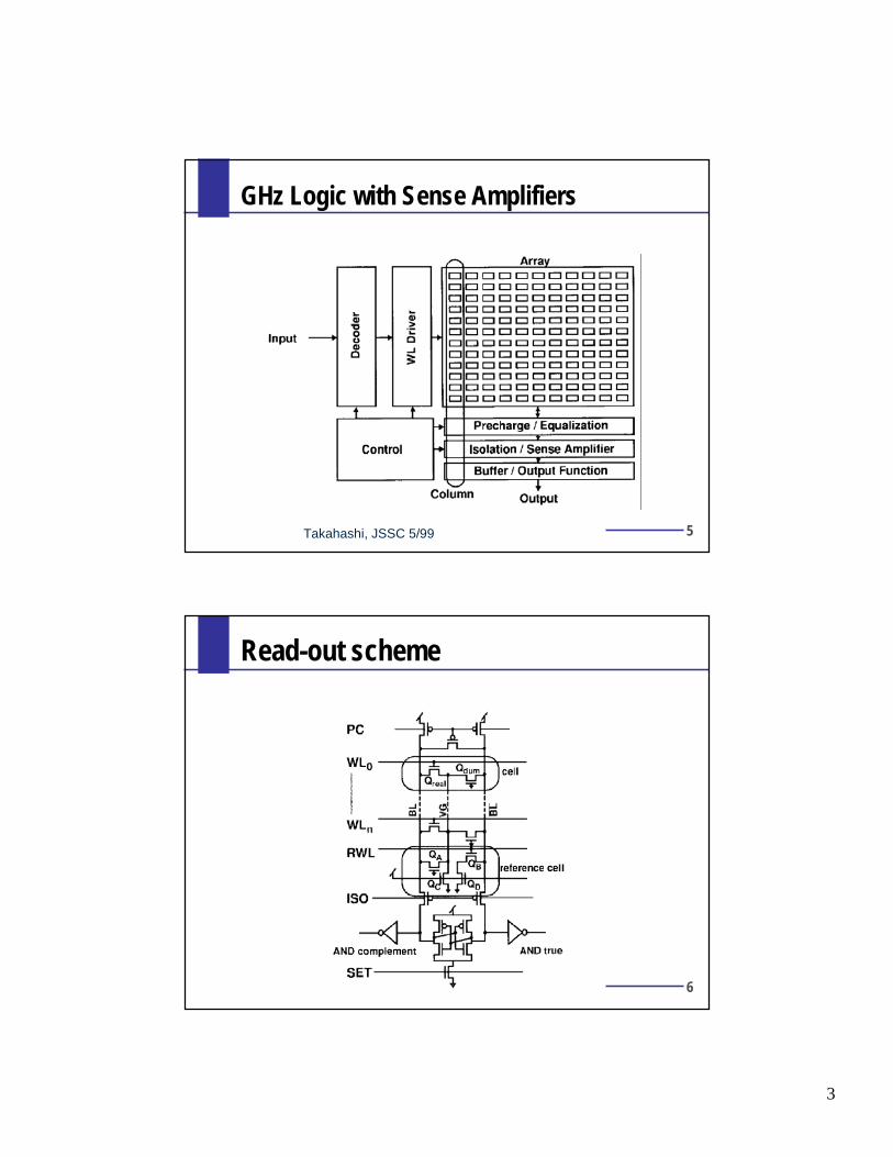
GHz Logic with Sense Amplifiers
Takahashi, JSSC 5/99
6
Read-out scheme

4
7
Implemented Macros
8
Rotator (ROT)
5
9
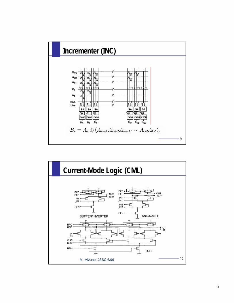
Incrementer (INC)
10
Current-Mode Logic (CML)
M. Mizuno, JSSC 6/96

6
11
Current-Mode Logic (CML)
12
Current-Mode Logic (CML)
7
Optimization for Power
14
The Importance of Power Awareness
Crucial for Portable ApplicationsDetermines battery lifetime
Increased amount of computation
Crucial for High-Performance ApplicationsDetermines cooling and energy costs
Many designs today are power limited
Still need maximum performance

8
15
The Power Challenge
Source: Roger SchmidtIBM Corp
K. Yazawa, Sony
16
Mobility:Battery storage the limiting factor
Little change in basic technologystore energy using a chemical reaction
Battery capacity doubles every 10 years
Energy density/size, safe handling are limiting factor
Energy densityof material
KWH/kg
Gasoline 14
Lead-Acid 0.04
Li polymer 0.15

9
17
Battery Progress
020406080
100120140160
1940 1950 1960 1970 1980 1990 2000 2010
First Commercial Use
Energy Density(Wh/kg)
Trend Line
NiCd SLA NiMH Li-Ion ReusableAlkaline
Li-Polymer
Facture 4 over the last 10 years!
18
Fuel cell may increase stored energymore than a order of magnitude
Du
rati
on
[H
ou
r]
Lithium IonBattery
1 10 100 10001
10
100
1000
10000
Output [W]
Direct Methanol Fuel Cell
NotePC
PDA
Cellular
Courtesy Toshiba

10
19
What can one do with 1 cm3?Energy Storage
3.2100Ultra-capacitor
341080Secondary battery
902880Primary battery
1103500Micro Fuel cell
µW/cm3/yearJ/cm3
20
What can one do with 1 cm3?Energy Generation
40Temperature
17Pressure Var.
10Solar (inside)
200Vibration
330Human power
380Air flow
15,000Solar (outside)
µW/cm3

11
21
What can one do with 1 cm3? Reference case: the human brain
Pavg(brain) = 20 W (20% of the total dissipation, 2% of the weight),
Power density: ~15 mW/cm3
Nerve cells only 4% of brain volume Nerve cells only 4% of brain volume Average neuron density: 70 million/cmAverage neuron density: 70 million/cm33
22
What can one do with 1 cm3? Perform computations …
300 million 4 input NAND gates (90 nm)7 million “Xilinx gates” (90 nm)Assuming 500 MHz clock frequency, 1V Vdd and fanoutof 4 and 10% activity:
15 Peta gate-ops/sec @ 45 WReducing supply voltage to 0.2V and clock rate to 10 MHz: 300 Giga gate-ops @ 40 mW

12
23
Outline
1. Know your enemy: Power consumption in CMOS
2. Leakage is here to stay
3. Power and performance are tightly coupled and have to be jointly optimized
4. Principles of Power Minimization
24
1. Know Your Enemy
Where does power go in CMOS?
Switching powerCharging capacitors
Leakage powerTransistors are imperfect switches
Short-circuit powerBoth pull-up and pull-down on during transition
Static currentsBiasing currents

13
25
Dynamic Power Consumption
One half of the power from the supply is consumed in the pull-up network and one half is stored on CL
Charge from CL is dumped during the 1→0 transition
Vdd
Vout
iL
CL
PMOS
NETWORK
NMOS
A1
AN
NETWORK
210 DDLVCE =→
2
21
DDLR VCE =
2
21
DDLC VCE =
26
Circuits with Reduced Swing
C L
V dd
V dd
V dd -V Th
( )ThDDDDL VVVCE −=→10

14
27
Dynamic Power Consumption
Power = Energy/transition • Transition rate
= CLVDD2 • f0→1
= CLVDD2 • f • P0→1
= CswitchedVDD2 • f
Power dissipation is data dependent – depends on the switching probabilitySwitched capacitance Cswitched = CL • P0→1
28
Transition Activity and Power
Energy consumed in N cycles, EN:
EN = CL • VDD2 • n0→1
n0→1 – number of 0→1 transitions in N cycles
fVCN
nf
NE
P DDLN
N
Navg ⋅⋅⋅⎟⎠⎞
⎜⎝⎛=⋅= →
∞→∞→
210limlim
fN
nN
⋅= →
∞→→10
10 limα
fVCP DDLavg ⋅⋅⋅= →2
10α

15
29
Type of Logic Function: NOR vs. XOR
011
001
010
100
OutBA
Example: Static 2-input NOR Gate
Assume signal probabilitiespA=1 = 1/2pB=1 = 1/2
Then transition probabilityp0→1 = pOut=0 x pOut=1
= 3/4 x 1/4 = 3/16
α0→1 = 3/16
If inputs switch every cycle
30
Type of Logic Function: NOR vs. XOR
011
101
110
000
OutBA
Example: Static 2-input XOR Gate
Assume signal probabilitiespA=1 = 1/2pB=1 = 1/2
Then transition probabilityp0→1 = pOut=0 x pOut=1
= 1/2 x 1/2 = 1/4
α0→1 = 1/4
If inputs switch in every cycle

16
31
Transition Probabilities
P0->1(NOR,NAND) = (2N-1)/22N P0->1(XOR) = 1/4
32
Transition Probabilities for Basic Gates
(1 - (pA +pB – 2pApB))(pA + pB – 2pApB)XOR
(1 - pA)(1 - pB)(1 - (1 - pA)(1 - pB))OR
(1 - pApB)pApBAND
p0→1
Transition probabilities for static CMOS gatesp0→1 = p0p1

17
33
Problem: Reconvergent Fanout
A
B
X
Z
Reconvergence
P(Z = 1) = P(B = 1) . P(X = 1 | B=1)
Becomes complex and intractable fast
34
Inter-Signal Correlations
Logic withoutreconvergent fanout
Logic with reconvergent fanout
A
BZ
CA
Z
C
B
p0→1 = (1 – pApB) pApBP(Z = 1) = p(C=1 | B=1) p(B=1)
p0→1 = 0
Need to use conditional probabilities to model inter-signal correlations
CAD tools required for such analysis

18
35
Glitching in Static CMOS
A
B
X
CZ
ABC 101 000
X
Z
Gate Delay
Also known asdynamic hazards
The result is correct,but there is extra power dissipated
36
Example: Chain of NOR Gates
1Out1 Out2 Out3 Out4 Out5
0 200 400 6000.0
1.0
2.0
3.0
Time (ps)
Voltage
(V) Out8
Out6
Out2
Out6
Out1
Out3
Out7
Out5

19
37
Short Circuit Current
Short circuit current is usually well controlled
Large load Small load
VinVout
CL
VDD
Isc ∼ 0
VinVout
CL
VDD
Isc = IMAX
0 20−0.5
0
0.5
1
1.5
2
2.5
40 60
I
sc
(A)
x 10−4
CL = 20 fF
CL = 100 fF
CL = 500 fF
time (s)
38
2. Transistors Leak
Drain leakageDiffusion currents
Drain-induced barrier lowering
Junction leakagesGate-induced drain leakage
Gate leakageTunneling currents through thin oxide

20
39
Transistor Leakage
-9
-8
-7
-6
-5
-4
-3
0 0.2 0.4 0.6 0.8 1 1.2
V GS [V]
log
I DS
[lo
g A
]
Subthreshold slope S = kT/q ln10 (1+Cd/Ci)
Drain leakage current is exponential with VGSSubthreshold slope is ~70mV/dec
VDS = 1.2V
G
S D
Sub
Ci
Cd
40
Transistor Leakage
Two effects:• diffusion current (like a bipolar transistor)• exponential increase with VDS (DIBL)
3-10x in current
technologies
0
2
4
6
8
0 0.2 0.4 0.6 0.8 1 1.2 1.4
V DS [V]
I DS
[nA
]
21
41
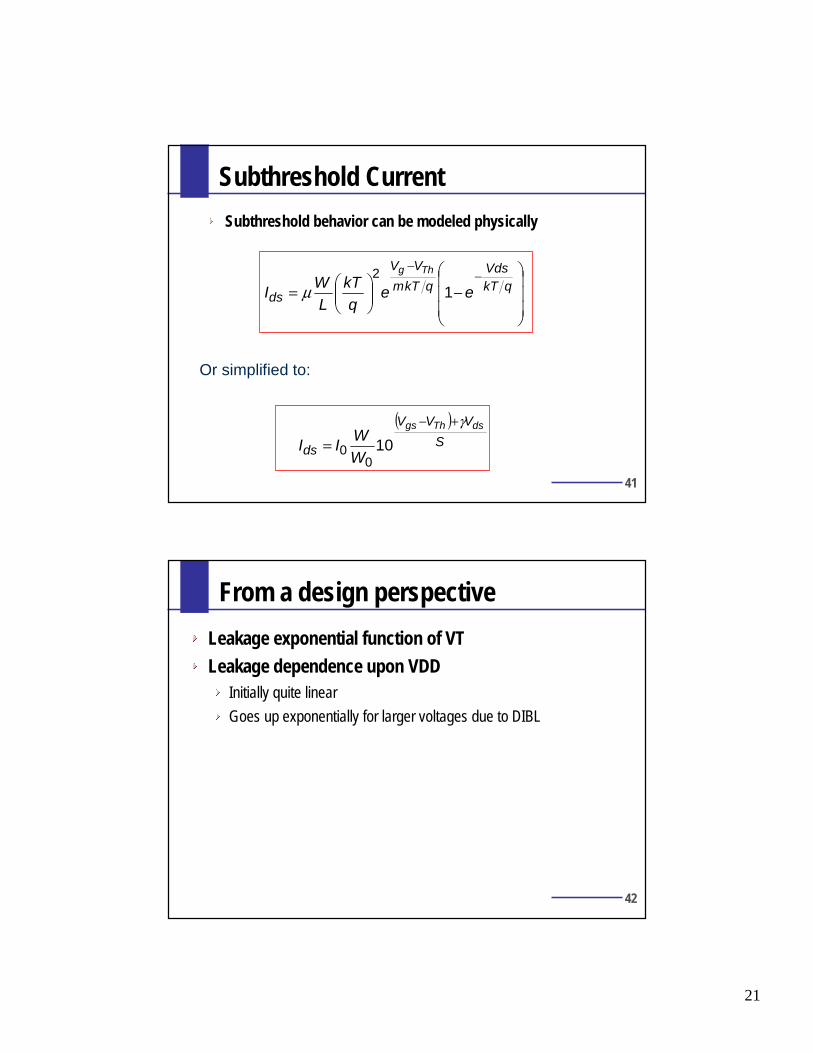
Subthreshold Current
Subthreshold behavior can be modeled physically
⎟⎟⎟
⎠
⎞
⎜⎜⎜
⎝
⎛−⎟⎟
⎠
⎞⎜⎜⎝
⎛=−
−qkT
VdsqkTm
VV
ds eeq
kTL
WI
Thg
12
µ
( )S
VVV
ds
dsThgs
WW
II
γ+−
= 100
0
Or simplified to:
42
From a design perspective
Leakage exponential function of VT
Leakage dependence upon VDDInitially quite linear
Goes up exponentially for larger voltages due to DIBL

22
43
Gate Leakage
Courtesy of IEEE Press, New York. © 2000
Trends Tunneling at thin oxides
44
Gate Tunneling
IGD~ e−ToxeVgd,
IGS~ e−ToxeVgs
Independent of the sub-threshold leakage
Contributes to the total leakage
Modeled in BSIM4Also in BSIM3v3 but foundries usually do not include it
NMOS gate leakage usually worse than PMOS
VDD 0V
VDD
ISUB
IGD
IGS
ILeak

23
45
Power /Energy Optimizaton Space
+ Variable VT
Sleep T’s
Multi-VDD Variable VT
+ Input control
Stack effects
+ Multi-VTLeakage
DFS, DVSClock Gating
Logic design
Scaled VDD
TSizing
Multi-VDD
Active
Run TimeSleep ModeDesign TimeEnergy
Variable Throughput/LatencyConstant Throughput/Latency
46
Reducing active power
Downsizing transistors (CL)Slows down logic
Lowering the supply voltage (VDD)Slows down logicReducing swing slows down the succeeding stage
Reducing frequency (f)Does not reduce energy
Reducing switching activity (α)Logic restructuring
Reducing glitchingBalancing logic
fVVCP DDswingLdyn ⋅⋅⋅⋅α~
DDswingL VVCE ⋅⋅⋅α~

24
47
Power : P = pt •fCLK •CL • VDD + 2 I0 •10 •VDD
VTH
S Delay :k • CL • VDD
(VDD - VTH)1.3= D
12
34
-0. 400.40.8
0
0.2
0.4
0.6
0.8
1x 10
-4
VTH (V)
VDD (V)
Pow
er (
W)
A
B
12
34
-0.400.40.8
0
1
2
3
4
5x 10
-10
Del
ay (
s)VTH
(V)VDD (V)
AB
Power is reduced while delay is unchanged if both VDDand VTH are lowered such as from A to B.
Relationship Between Power and Delay
[From Kuroda]
48
Reducing Active Power
Downsizing, lowering the supply on the critical path will lower the operating frequency
Downsize non-critical pathsNarrows down the path delay distributionIncreases impact of variations
Delay
Pat
h co
unt Target
delay
Original delaydistribution

25
49
Multi-Level Approach
Energy minimization subject to delay constraint
Optimal trade-off between energy and area
Architecture
Micro-Architecture
Circuit (Logic & FFs)
EnergyEnergy--Area (Cost) Area (Cost) ––PerformancePerformance
EnergyEnergy--PerformancePerformance
EnergyEnergy--DelayDelay
50
LiteratureBooks:
J. Rabaey, A. Chandrakasan, B. Nikolic, “Digital Integrated Circuits: A Design Perspective,” 2nd ed, Prentice Hall 2003.
A. Chandrakasan, W. Bowhill, F. Fox (eds.), “Design of High-Performance Microprocessor Circuits”, IEEE Press 2001.
Chapter 4, Low-Voltage Technologies, by Kuroda and Sakurai
Chapter 3, Techniques for Leakage Power Reduction, by De, et al.
A. Chandrakasan and R. Brodersen, “Low Power CMOS Design”, Kluwer Academic Publishers, 1995.
J. Rabaey and M. Pedram, Ed., “Low Power Design Methodologies”, Kluwer Academic Publishers, 1995. 2nd ed, 2002.
A. Chandrakasan and R. Brodersen, “Low-Power CMOS Design”, IEEE Press, 1998 (Reprint Volume)

26
51
LiteratureArticles:
A. P. Chandrakasan and R. W. Brodersen, “Minimizing power consumption in digital CMOS circuits,” Proceedings of the IEEE, no.4, p.498-523, April 1995.
A.P. Chandrakasan, S. Sheng, R.W. Brodersen, Low-power CMOS digital design. IEEE Journal of Solid-State Circuits, vol.27, no.4, p.473-84, April 1992.
T.Kuroda, T. Sakurai, “Overview of low-power ULSI circuit techniques,” IEICE Trans. on Electronics, vol. E78-C, no. 4, pp. 334-344, April 1995.
S. Borkar, “Design challenges of technology scaling,” IEEE Micro, vol.19, no.4, p.23-29, July-Aug. 1999.


![Analysis of 6T FinFET SRAM Assist Techniques and …djseo/classes/ee241/...EE241 Final Report 2 (a) (b) (c) Fig. 1 FinFET-based SRAM cell array published by [1]. High Density Cell](https://static.fdocuments.in/doc/165x107/5ae6f2697f8b9a6d4f8d666f/analysis-of-6t-finfet-sram-assist-techniques-and-djseoclassesee241ee241.jpg)

