DEPARTMENT WAFER LEVEL SYSTEM INTEGRATION · DEPARTMENT WAFER LEVEL SYSTEM INTEGRATION ALL SILICON...
6
FRAUNHOFER INSTITUTE FOR RELIABILITY AND MICROINTEGRATION IZM DEPARTMENT WAFER LEVEL SYSTEM INTEGRATION ALL SILICON SYSTEM INTEGRATION DRESDEN – ASSID
Transcript of DEPARTMENT WAFER LEVEL SYSTEM INTEGRATION · DEPARTMENT WAFER LEVEL SYSTEM INTEGRATION ALL SILICON...
F R A U N H O F E R I N S T I T U T E F O R R E L I A B I L I T Y A N D M I C R O I N T E G R AT I O N I Z M
DEPARTMENT WAFER LEVEL SYSTEM INTEGRATIONALL SILICON SYSTEM INTEGRATION DRESDEN – ASSID

FRAUNHOFER IZM
The Fraunhofer Institute for Reliability and Microintegration (IZM) belongs to
the Fraunhofer Group for Microelectronics. The Fraunhofer-Gesellschaft is one
of the leading organizations of applied research in Europe undertaking contract
research on behalf of industry. Fraunhofer IZM is a worldwide renowned institute
specializing in developing advanced packaging and system integration technolo-
gies and transferring research results to the industry and thus being able to offer
customer-specific solutions for microelectronic products in the overall scope of
smart system integration.
FRAUNHOFER IZM-ASSID
Fraunhofer IZMs center “All Silicon System Integration Dresden – ASSID” operates
a leading edge, industry-compatible 200/300 mm 3D wafer-level process line with
modules for TSV formation, pre-assembly (thinning, singulation), wafer-level assem-
bly and stack formation. ASSID is focusing on process development, material and
equipment evaluation as well as R&D services. It is a partner in national, European
and worldwide industrial and scientific projects and networks for 3D system integra-
tion, e. g., HIR, HTA, ENIAC JU, Catrene, EPOSS, SEMATECH and the Silicon Saxony
Network. Fraunhofer IZM-ASSID has established cooperation and joint development
programs with industrial partners for undertaking material and equipment evalua-
tion, process development as well as process and product integration.
COOPERATION ACTIVITIES
Within the realms of academia, IZM-ASSID is cooperating with
• Technische Universität Dresden (Electronic Packaging Laboratory, IAVT)
• Technische Universität Chemnitz
Fraunhofer IZM-ASSID has established close collaborations especially among the Saxony-based Fraunhofer Institutes. Besides
joint projects and services, these activities include:
• Fraunhofer Clustr 3D Integration: To cope with the technological complexity of 3D integration, leading Fraunhofer in-
stitutes cluster their outstanding competencies in the fields of technology, design, analytics and reliability to cover a broad
spectrum of topics and approaches. For this continuous commitment, the Cluster received the 3DInCites Award “Research
Institute of the Year” in July 2016. www.3D-integration.fraunhofer.de
• High Performance Centre „Funktionsintegration Mikro-/Nano-Elektronik“ //
High Performance Center Functional Integration in Micro- and Nanoelectronics:
Fraunhofer, TU Dresden and TU Chemnitz cluster their competencies in the fields of micro / nano electronics and thus strength-
en the competitive and innovative capacity of the Free State of Saxony. Research know-how will – in close cooperation with
resident companies – be extended and innovations can be implemented more quickly into applications and products.
Cover picture: 9x TSV Chip Stack on 300 mm Base Wafer
ALL SILICON SYSTEM INTEGRATION DRESDEN FRAUNHOFER IZM-ASSID
22

3
HETEROGENEOUS 3D WAFER-LEVEL SYSTEM INTEGRATION3D integration is of high significance for the realization of future innovative
products and a key enabler to meet technical requirements e.g. performance,
form factor and functionality for smart systems in application fields like informa-
tion & communication, security, healthcare, mobility & transportation and
industrial electronics. It allows the multi-device integration of analog and digital
devices e. g. sensors, MPU, ASICs and transceivers into one optimized wafer-level
system in package (WL-SiP). Therefore, scientific & industrial research is focusing
on developing 3D integration technologies to enable 3D smart systems.
3D Wafer-level System in Package Pilot Line
Fraunhofer IZM-ASSID provides prototyping and low-volume manufacturing
services (300/200 mm) at its leading-edge pilot line for wafer-level packaging.
Fraunhofer IZM-ASSID has established strong cooperations with leading mate-
rial and equipment suppliers in which customer-specific solutions in the fields of
material, equipment and processes are developed and introduced into products.
As a member of the Fraunhofer Cluster 3D Integration, Fraunhofer IZM-ASSID
offers – together with its Fraunhofer partners – fully customized support for 3D
integration including design, technology and reliability.
Core Competencies:
• Leading-edge micro-electronic packaging
• 3D heterogeneous system integration
• Wafer-level System-in-Packages (WL-SiP)
• Enhanced interconnection & assembly
technologies
• Customized technology development
• Customer-specific prototyping & pilot-line
manufacturing
• Process, equipment & material evaluations
as well as qualification
• Process transfer & product integration
ROADMAP – 3D INTEGRATED SYSTEMS
3D
IN
TE
RC
ON
NE
CT
CO
MP
LE
XIT
Y
2 0 1 1 2 0 1 3 2 0 1 5 2 0 1 7 2 0 1 9 Y E A R
CHIP STACK (D2IP)
MULTIPLEIC/IP STACKS
WIRELESSSENSOR NODES
3D HETERO-GENEOUS SYSTEMS
3D IMAGESENSORS
3D IP-SiP
3D SIPELECTR./OPT.
3D WL-SIPMULTI-SENSOR
3D IC STACK
eGRAIN
3D PERFORMANCE CPU WITH ACTIVE COOLING
WLP OPTO PACKAGE
CSP/WLP IPD
© Fraunhofer IZM 9-2013
MEMORY STACK
4
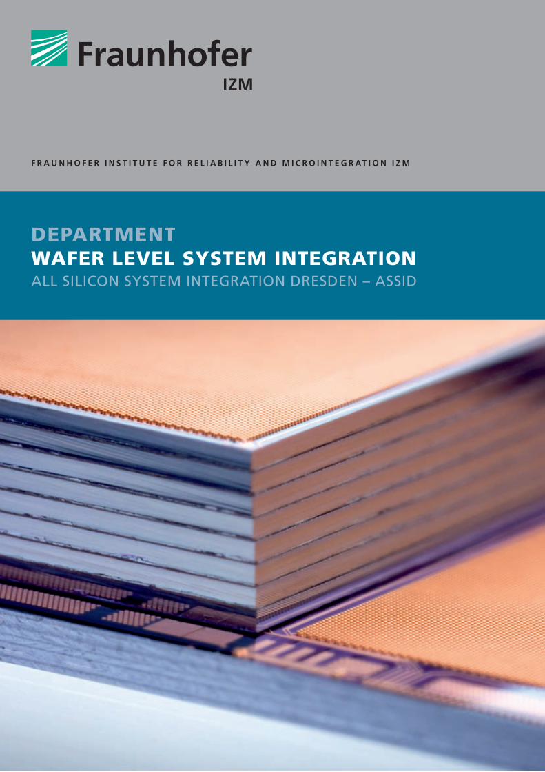
COPPER THROUGH SILICON VIA (TSV)FORMATION Through silicon Vias (TSVs) are a key element in 3D wafer-level
system integration. Fraunhofer IZM-ASSID has developed a
TSV process (POR) for customer-defined applications based on
Cu-ECD.
All processes are carried out using leading-edge, industry-
compatible process equipment for 200 / 300 mm wafers.
Capabilities and research focus:
• High-density Cu-TSV technology (via-last, via-middle,
backside via-last) for active circuit devices and interposers
• Application-specific TSV dimensions diameter/depth:
… min. 5 μm / 50 μm
… typ. 10 μm / 120 μm
… 20 μm / 120 μm
… backside TSV (Cu-liner) up to 250 – 700 μm depth
• Cu-TSV filling using high-speed ECD
• Evaluation and qualification of new materials for isolation,
barrier / seed and TSV filling
• Optimized via reveal
WAFER THINNING, AND THIN WAFER HANDLING Wafer thinning and thin wafer handling technologies are an
integral part of the TSV process integration as well as essential
for the realization of 3D system architectures.
Continuous optimization of these technologies is indispens-
able to meet the requirements of cost-effective manufacturing
and the realization of 3D systems.
Capabilities and research focus:
• Optimization of temporary wafer-bonding and de-bonding
technologies (device wafer thickness: > 20 μm; multiple
repeatable bonding and de-bonding processes)
• Enhanced wafer thinning and stress relief technologies for
ultra-thin wafers (> 20 μm)
• Enhanced dicing technologies using low k-materials, small
dicing streets (< 40 μm) and reduced mechanical edge and
corner damage to wafer frontside and backside

5
TSV-INTERPOSER WITH HIGH-DENSITY REDISTRIBUTION The TSV interposer is used as a carrier to meet the technical
specifications of integrated circuits e.g., geometry, high number
of I/O and their high-density routing. According to the ap-
plication, multi-layer high-density wiring on frontside/backside
down to < 2 μm line/space as well as Cu-TSVs with diameters
between 5 – 20 μm are required. The functionality of Si-inter-
posers will be extended by the integration of passive devices
such as inductors, resistors and capacitors – with an emphasis
on RF applications. Next generations will also include integrated
active devices and deal with high power dissipation by applying
innovative cooling architectures and will also address the
integration of electrical/optical interconnects for high speed
data transmission. These new generations of Si-interposers are
the basic prerequisite for modularized 3D stacked architectures
for fully heterogeneous system integration.
Capabilities and research focus:
• Interposers with high-density Cu-TSV
• High-density multi-layer copper wiring: > 2 µm line/space,
4-layer frontside RDL, up to 3-layer backside RDL
• Integration of passive devices (R, L, C)
• Embedding of active and passive devices
• Interconnects for 3D stacking of devices/substrates
• Thermal management
3D-ASSEMBLY AND INTERCONNECTION TECHNOLOGIESAssembly and interconnection technologies relevant for 3D
system integration are strongly affected by IC technology
nodes. Key parameters include die size, number of I/O, pad
geometries, passivation layers, wafer-surface topologies,
terminal pads and limitations to the thermal budgets that can
be applied during assembly. Additional challenges in assembly
and interconnect technologies for 3D systems include align-
ment accuracy, yield requirements and productivity that meet
the demands of cost effective manufacturing.
Capabilities and research focus:
• Evaluation of die-to-wafer (D2W), die-to-interposer (D2IP)
and wafer-to-wafer (W2W) assembly technologies
• 3D IC assembly with high-density interconnects (> 1000 I/O)
and ultra-fine pitch (> 50 μm)
• IC assembly with thin and ultra-thin chips (20 – 150 μm)
• Evaluation of low-temperature assembly technologies
• Evaluation of flux-free solder connections with
self-alignment capability
• 3D stack formation
CONTACT
Director Fraunhofer IZM
Prof. Dr. Klaus-Dieter Lang
Phone: +49 (0)30 46403 153
E-mail: [email protected]
All Silicon System Integration Dresden – ASSID
Fraunhofer IZM-ASSID
Ringstr. 12
01468 Moritzburg, Germany
Phone: +49 (0)351 795572 0
www.izm.fraunhofer.de/assid
Management IZM-ASSID
Head of Division Wafer Level System Integration
M. Jürgen Wolf
Phone: +49 (0)351 795572 12
E-mail: [email protected]
Project Management & Development
Thomas Werner | +49 (0)351 795572 915
E-mail: [email protected]
TSV Process Integration
René Puschmann | +49 (0)351 795572 45
E-mail: [email protected]
Backend-of-Line and Metrology
Dr. Mathias Böttcher | +49 (0)351 795572 40
E-mail: [email protected]
Wet Processing
Catharina Rudolph | +49 (0)351 795572 61
E-mail: [email protected]
Pre-Assembly & Assembly
Dr. Jürgen Grafe | +49 (0)351 795572 60
E-mail: [email protected]
Nanomaterials (Cooperation with TU Dresden/IAVT)
Jun.- Prof. Dr. Iuliana Panchenko | +49 (0)351 795572 814
E-mail: [email protected] Con
cept
& E
ditin
g: F
raun
hofe
r IZ
M P
ress
and
Pub
lic R
elat
ions
, Ber
lin +
MC
C G
mbH
Ber
lin ·
Des
ign:
J. M
etze
, Ber
lin ·
Pho
togr
aphy
: Fra
unho
fer
IZM
tog
ethe
r
with
: IK
TS-M
D/d
fcna
(p
4 to
p rig
ht),
N. H
alm
(p. 6
left
), N
. Kör
ner
(p. 3
bot
tom
rig
ht),
V. M
ai (f
ront
, p. 2
, top
, p. 4
, 2nd
fro
m le
ft)
ASS
ID 1
7/05
-08e
CUSTOMERSERVICESTechnological services include:
• Customer-specific prototyping (WL-SiP, TSV interposer) and
pilot line manufacturing
• Material and equipment evaluation, process development,
process transfer and product integration
• TSV silicon interposer
• 3D TSV via middle/via last process integration
• Deposition & patterning of dielectric polymers and metal films
• Multi-layer Cu redistribution with customer-specific terminal
pad metallurgies (Cu, Cu/Ni/Au, Cu/SnAg)
• Wafer thinning and thin wafer processing
• ECD WL bumping (Cu-Pillar, SnAg, CuNiAu)
• WL assembly (D2W, W2W)
Fraunhofer IZM-ASSIDs ISO 9001
certified management system guarantees
high quality standards for its industrial services.
The Fraunhofer Cluster 3D Integration
received the 3DInCites Award
“Research Institute of the Year” in 2016.
izmassid
IZM-ASSID
Fraunhofer IZM-ASSID is supported by the Federal Ministry of Education and Research,
the Free State of Saxony and the European Commission.