Maria Berdova Postgraduate Course in Electron Physics I [email protected] 1.
Upload
nigel-carrollCategory
view
218download
2
Wafer selection
• active role for the wafer ?• passive role ?
– thermal conductivity– optical transparency– flat, smooth mechanical support
• compatibility with equipment ?• thermal limitations ?• contamination ? Especially glass in Si fabs !

Metal heater processing
1. Metal sputtering (or evaporation)
2. Photoresist spinning & baking
3. Lithography with resistor mask
4. Resist image development
5. Metal etching
6. Photoresist strippingCan be done on any wafer !
Glass wafers, polymer, ...
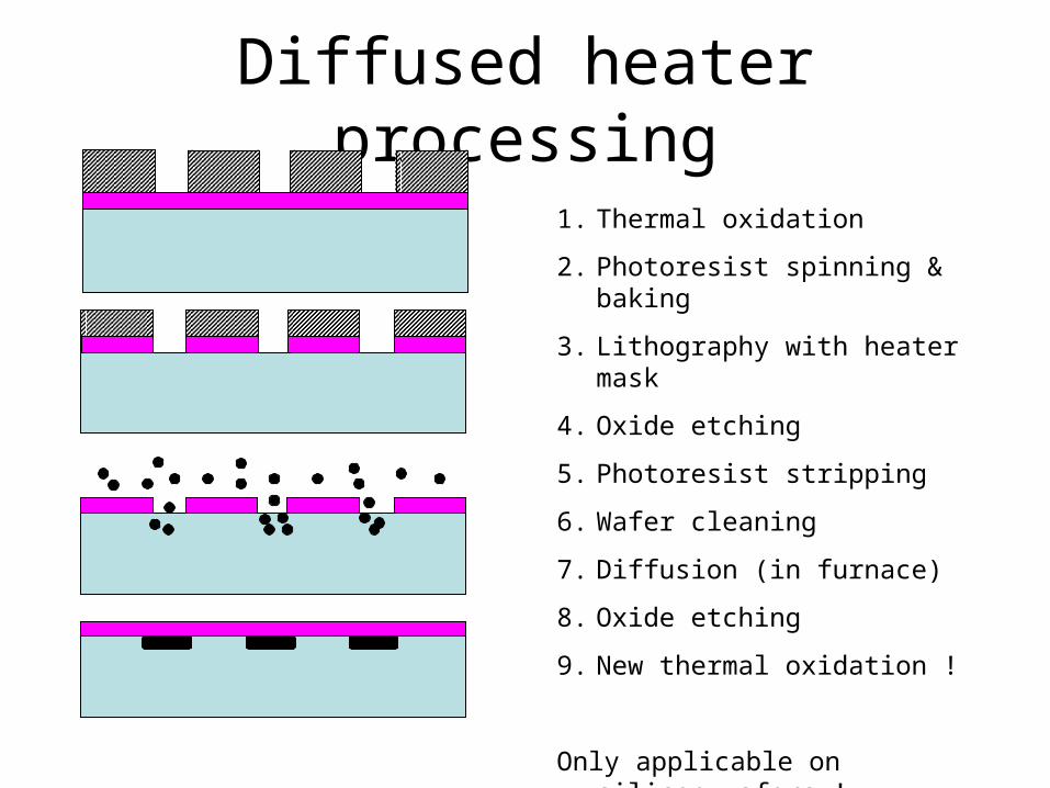
Diffused heater processing
1. Thermal oxidation
2. Photoresist spinning & baking
3. Lithography with heater mask
4. Oxide etching
5. Photoresist stripping
6. Wafer cleaning
7. Diffusion (in furnace)
8. Oxide etching
9. New thermal oxidation !
Only applicable on silicon wafers !
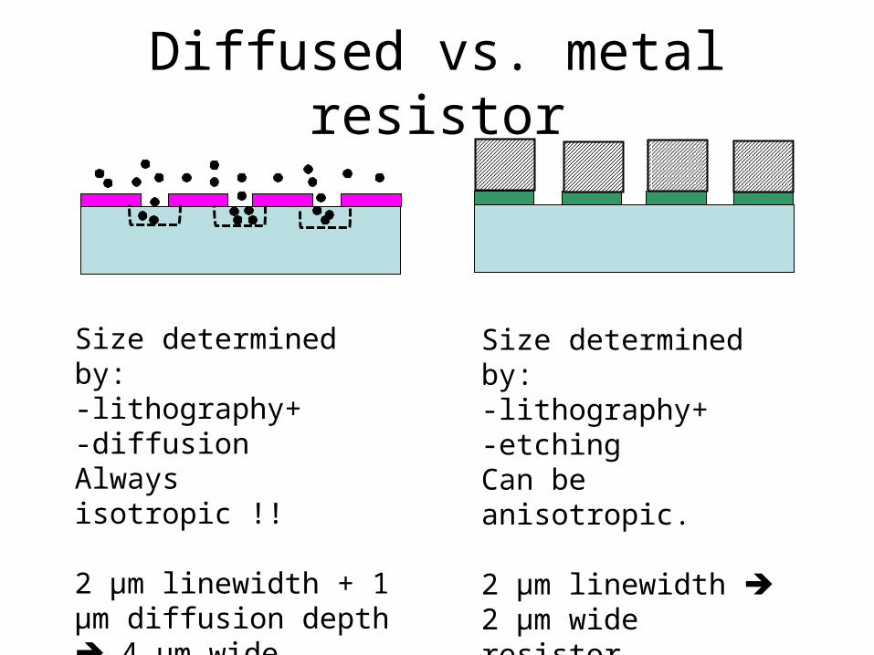
Diffused vs. metal resistor
Size determined by:-lithography+-diffusionAlways isotropic !!
2 µm linewidth + 1 µm diffusion depth 4 µm wide resistor
Size determined by:-lithography+-etchingCan be anisotropic.
2 µm linewidth 2 µm wide resistor

Example:solar cell process flow
top metallization
anti-reflectivecoating (ARC)
Backside metallization
p-substrate
p+ diffusion
n -diffusion
The contact holes in anti-reflective coating are non-critical
The metallization alignment to contact holes is critical
(in case of misalignment, metal does not fully cover holes, and gases, liquids, dirt can penetrate into silicon)
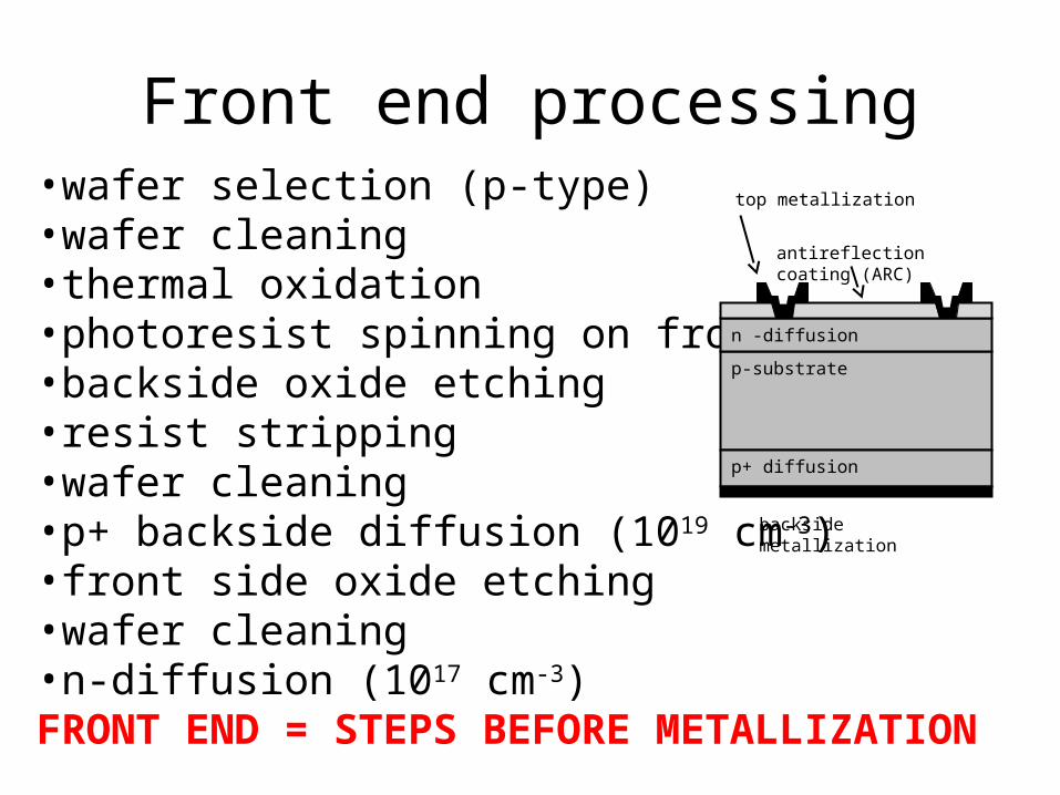
Front end processing•wafer selection (p-type)•wafer cleaning•thermal oxidation•photoresist spinning on front•backside oxide etching•resist stripping•wafer cleaning•p+ backside diffusion (1019 cm-3)•front side oxide etching•wafer cleaning •n-diffusion (1017 cm-3)FRONT END = STEPS BEFORE METALLIZATION
backside metallization
top metallization
antireflection coating (ARC)
p-substrate
p+ diffusion
n -diffusion

Backend processing•resist spinning on front•metal sputtering on back side•resist stripping•wafer cleaning•PECVD nitride deposition•lithography for contact holes•etching of nitride•resist stripping•wafer cleaning•metal deposition on front side•lithography for front metal•metal etching•photoresist stripping•contact improvement anneal
backside metallization
top metallization
antireflection coating (ARC)
p-substrate
p+ diffusion
n -diffusion
BACKEND IS PROCESS AFTER FIRST METAL DEPOSITION

Active vs. passive cleaning
• Cleanroom (and its subsystems) provide passive cleanliness
• Wafer cleaning provides active cleaning

Wafer cleaning
• removal of added contamination
• ultrapure chemicals (very expensive)
• particle-free (filtered 0.3 µm)
• always includes rinsing & drying steps (with ultrapure water and nitrogen)

Surface preparation
• leaves wafer in known surface condition
• eliminates previous step peculiarities
• eliminates waiting time effects
• Wafer cleaning is the same as surface preparation; it is just a different viewpoint of wafer cleanliness
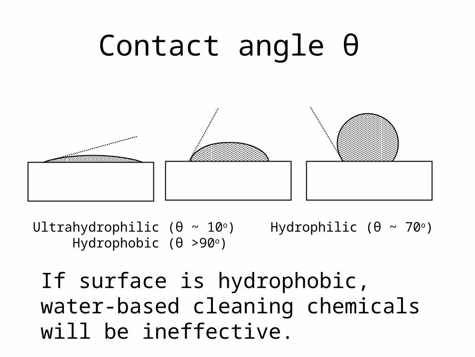
Contact angle θ
Ultrahydrophilic (θ ~ 10o) Hydrophilic (θ ~ 70o) Hydrophobic (θ >90o)
If surface is hydrophobic, water-based cleaning chemicals will be ineffective.

RCA-1 cleaning
• NH4OH:H2O2:H2O (1:1:5)
• removes particles
• removes organic (polymeric) materials
• leaves surface hydrophilic

RCA-2 cleaning
• HCl:H2O2:H2O (1:1:6)
• removes metal contamination
• leaves surface hydrophilic

Piranha: H2SO4 + H2O2
• H2SO4 is a strong oxidant
• oxidizing effect is enhanced by addition of peroxide H2O2
• Leaves surface with a thin SiO2 layer (= hydrophilic). Nitric acid similar.

HF, hydrofluoric acid
• removes SiO2
• leaves surface hydrophobic
Thermal oxidation + HF etching is a really good cleaning method !
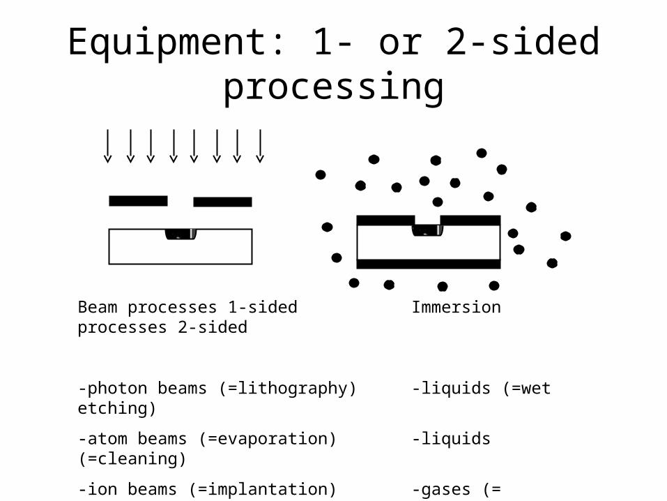
Equipment: 1- or 2-sided processing
Beam processes 1-sided Immersion processes 2-sided
-photon beams (=lithography) -liquids (=wet etching)
-atom beams (=evaporation) -liquids (=cleaning)
-ion beams (=implantation) -gases (= oxidation, diffusion)
-mixture of these (=plasmas) -gases (=CVD)

Both side processes
Thermal oxidationCVD
Wet etchingWet cleaning

Single side processes
PECVD, RIEIon implantation

Wet etch vs. plasma etch
Oxide wet etch in HF Oxide plasma etch in CHF3
Backside remains protectedFilm removed from backside
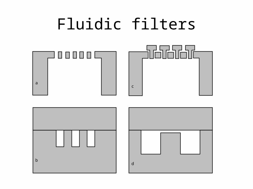
Fluidic filters
a
b
c
d

Fluidic filters (2)
Criteria:
Need one or two wafers ? Cost, bonding...
Pass size determined by litho ? Bonding ?
Flow resistance ? Aperture ratio.
Clogging ? Active cleaning ?
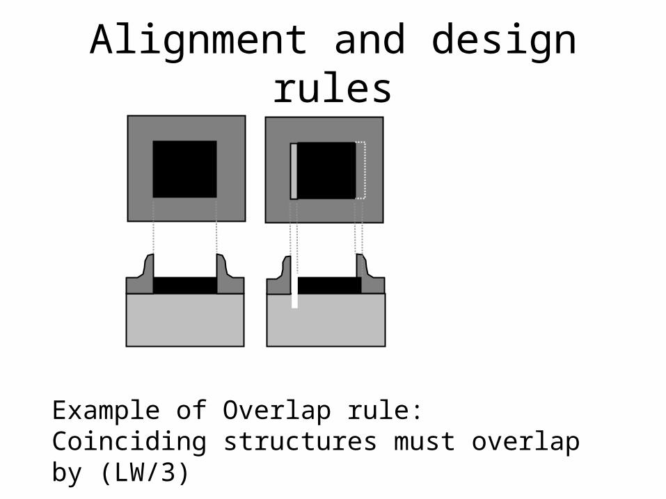
Alignment and design rules
Example of Overlap rule: Coinciding structures must overlap by (LW/3)
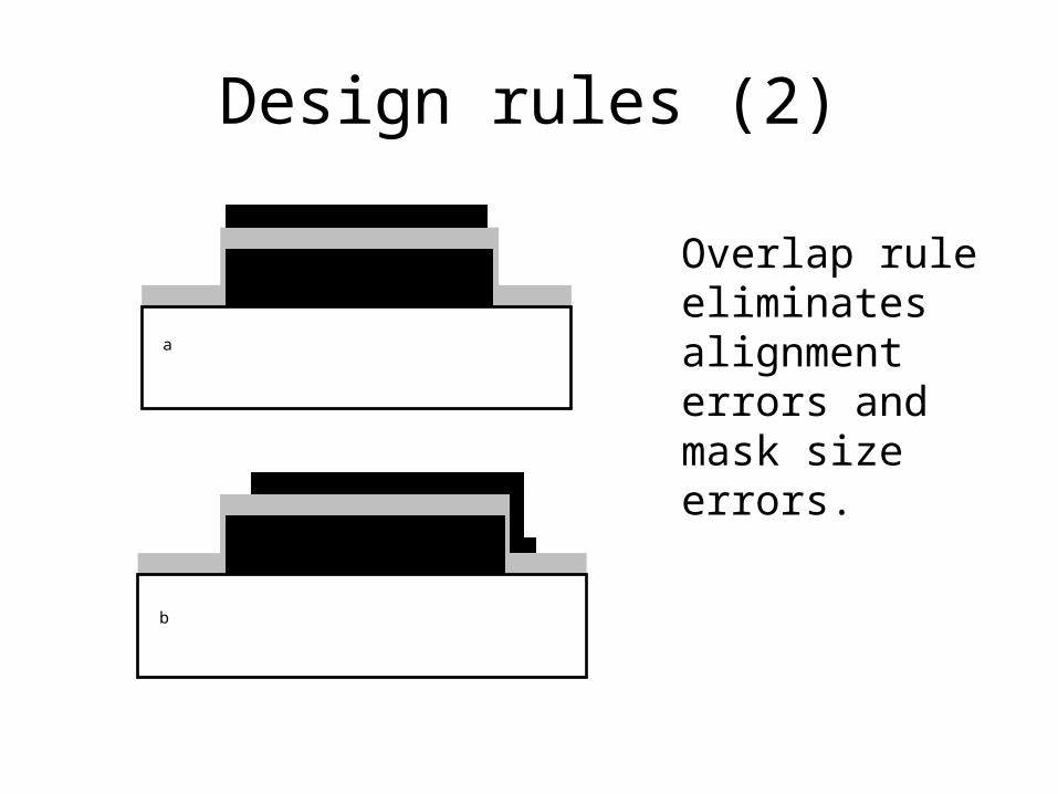
Design rules (2)
a
b
Overlap rule eliminates alignment errors and mask size errors.

Design rules (3)
Minimum linewidth ruleMinimum spacing rule
Overlap rules for structures on different layers
Electrical rules: Aluminum sheet rsistance 0.03 Ω/sqNo rectangular capacitors
Breaking design rules ruins your process(=you are expecting too much from the process)
Within one layer
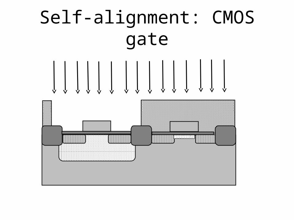
Self-alignment: CMOS gate
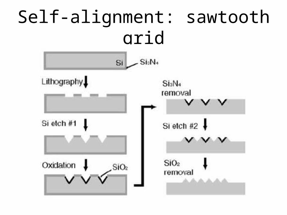
Self-alignment: sawtooth grid

RCL circuit on silica
CVD ox-1
CVD ox-2
fused silica
CVD ox-3
capacitor Mo resistor SiCr resistor
Au-coil
nitride

Cleaning steps omitted !!Wafer selection: fused silica to eliminate paracitic capacitanceMolybdenum depositionLithography #1: molybdenum resistor and capacitor bottom plateMolybdenum etching and resist strippingNitride deposition by LPCVDCVD oxide-1 depositionSputtering of SiCr high resistivity resistor
CVD ox-1
CVD ox-2
fused silica
CVD ox-3
capacitor Mo resistor SiCr resistor
Au-coil
nitride
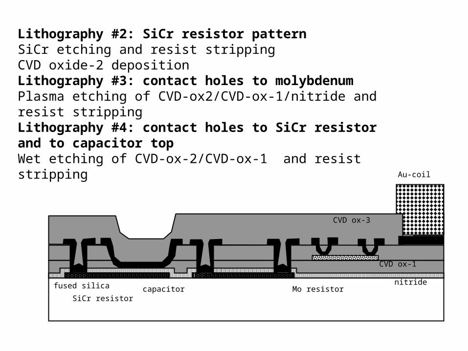
Lithography #2: SiCr resistor patternSiCr etching and resist strippingCVD oxide-2 depositionLithography #3: contact holes to molybdenumPlasma etching of CVD-ox2/CVD-ox-1/nitride and resist strippingLithography #4: contact holes to SiCr resistor and to capacitor topWet etching of CVD-ox-2/CVD-ox-1 and resist stripping
CVD ox-1
CVD ox-2
fused silica
CVD ox-3
capacitor Mo resistor SiCr resistor
Au-coil
nitride

Aluminum depositionLithography #5: aluminum patternAluminum etching and resist strippingCVD oxide-3 depositionLithography #6: contact holes to aluminumEtching of CVD-ox-3 and resist strippingLithography #7: Inductor coil patternGold electroplatingResist stripping
CVD ox-1
CVD ox-2
fused silica
CVD ox-3
capacitor Mo resistor SiCr resistor
Au-coil
nitride
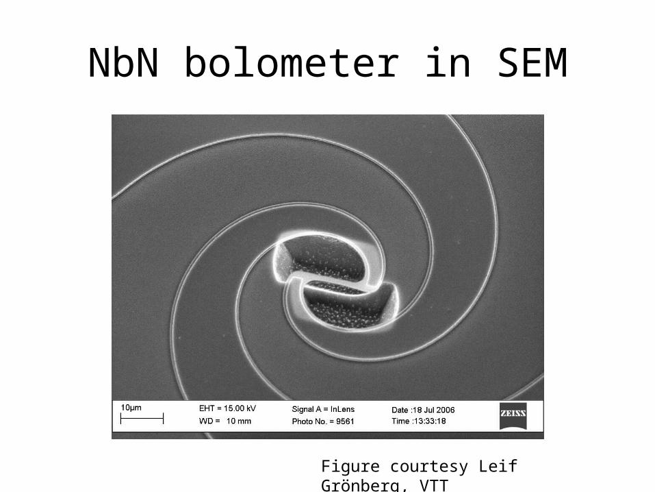
NbN bolometer in SEM
Figure courtesy Leif Grönberg, VTT
Bolometer mask view
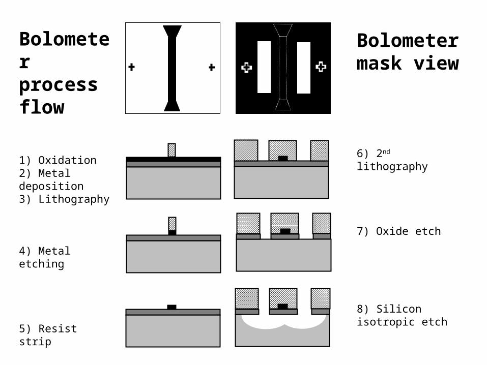
1) Oxidation2) Metal deposition3) Lithography
4) Metal etching
5) Resist strip
Bolometer process flow
6) 2nd lithography
7) Oxide etch
8) Silicon isotropic etch

NbN bolometer in SEM
Figure courtesy Leif Grönberg, VTT

NbN bolometer with Al pads
Optical microscope image
(top view)
Schematic drawing
top view
Schematic drawing
(side view)
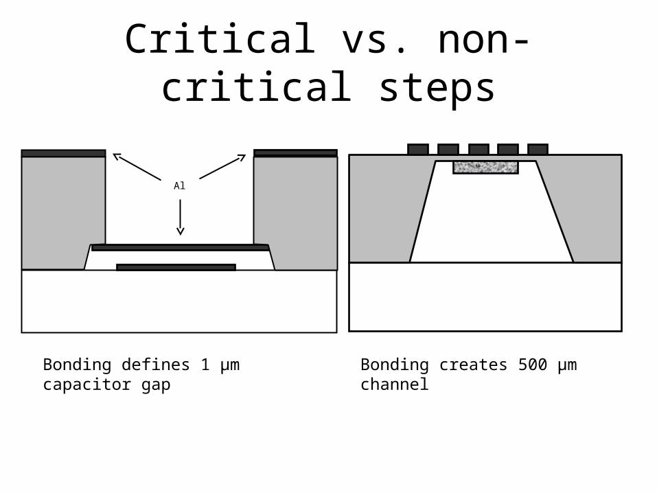
Critical vs. non-critical steps
Al
Bonding defines 1 µm capacitor gap Bonding creates 500 µm channel

Order of process steps

Order of process steps (2)

Protecting wafers
• from dirt ( cleanrooms & gowning)• from atoms, ions, molecules
( wafer cleaning)• from mechanics ( backside & edge
protection)• from chemicals ( compatibility)• from temperature ( thermal budget)• from static electricity (ESD shielding)