3D Integration Using Adhesive, Metal, and Metal/Adhesive as Wafer
13
3D Integration Using Adhesive, Metal, and Metal/Adhesive as Wafer Bonding Interfaces. Journal: 2008 MRS Fall Meeting Manuscript ID: 1112-E02-01.R1 Symposium: Symposium E Date Submitted by the Author: n/a Complete List of Authors: Lu, Jian-Qiang; Rensselaer Polytechnic Institute, Department of Electrical, Computer, and Systems Engineering; Center for Integrated Electronics McMahon, J.; Rensselaer Polytechnic Institute, Department of Electrical, Computer, and Systems Engineering; Center for Integrated Electronics Gutmann, Ronald; Rensselaer Polytechnic Institute, Department of Electrical, Computer, and Systems Engineering; Center for Integrated Electronics Keywords: bonding, electronic material, microelectronics
Transcript of 3D Integration Using Adhesive, Metal, and Metal/Adhesive as Wafer

3D Integration Using Adhesive, Metal, and Metal/Adhesive
as Wafer Bonding Interfaces.
Journal: 2008 MRS Fall Meeting
Manuscript ID: 1112-E02-01.R1
Symposium: Symposium E
Date Submitted by the Author:
n/a
Complete List of Authors: Lu, Jian-Qiang; Rensselaer Polytechnic Institute, Department of Electrical, Computer, and Systems Engineering; Center for Integrated Electronics McMahon, J.; Rensselaer Polytechnic Institute, Department of Electrical, Computer, and Systems Engineering; Center for Integrated Electronics Gutmann, Ronald; Rensselaer Polytechnic Institute, Department of Electrical, Computer, and Systems Engineering; Center for Integrated Electronics
Keywords: bonding, electronic material, microelectronics

3D Integration Using Adhesive, Metal, and Metal/Adhesive as Wafer Bonding Interfaces Jian-Qiang Lu1, J. Jay McMahon1,2 and Ronald J. Gutmann1,3 1 Department of Electrical, Computer, and Systems Engineering; Center for Integrated
Electronics, Rensselaer Polytechnic Institute, Troy, NY 12180. [email protected] 2 Current affiliation: GE Global Research Center, Niskayuna, NY 12309 3 Consultant and Professor Emeritus at Rensselaer Polytechnic Institute, Troy, NY 12180
ABSTRACT
Three-dimensional (3D) integration is an emerging technology that vertically stacks and interconnects multiple materials, technologies and functional components to form highly integrated micro/nano-systems. This paper reviews the materials and technologies for three wafer bonding approaches to 3D integration using adhesive, metal, and metal/adhesive as the bonding interfaces. Similarities and differences in architectural advantages and technology challenges are presented, with recent research advances discussed. INTRODUCTION
Three-dimensional (3D) hyper-integration* is an emerging technology that can form highly integrated systems by vertically stacking and connecting various materials, technologies, and functional components together [1, 2]. Figure 1 shows schematic representations of major 3D integration approaches pursued currently [1]. They can be divided into three categories based on their similarity to other technologies:
• 3D packaging technology (Fig. 1a-c); • Transistor build-up 3D technology (Fig. 1d-f); • Wafer-level, back-end-of-the-line (BEOL)-compatible 3D technology (Fig. 1g-k).
The potential benefits of 3D integration varies for each approach; they include multi-functionality, small form factor, increased speed and data bandwidth, reduced power, reduced component packaging, increased yield and reliability, flexible heterogeneous integration, and reduced overall costs. For example, a small form factor is achieved by stacking active component layers on top of one another in any 3D approach. Since classical CMOS device scaling has stalled, this third dimension would allow extending Moore’s law to ever higher density, higher functionality, and higher performance, while more diversified materials and devices can be integrated with lower cost. It could be expected that the industry paradigm will shift to a new era of 3D integration that will offer tremendous global opportunities for highly integrated systems. This paper provides a review of the materials and technologies for three wafer bonding approaches to monolithic, wafer-level, BEOL-compatible 3D integration using adhesive, metal, and metal/adhesive as the bonding interfaces [3-22]. Similarities and differences in architectural advantages and technology challenges are presented. Recent research advances and potential reliability issues are discussed. Other 3D approaches beyond the scope of this manuscript are covered elsewhere [1]. * The term ‘hyper-integration’ means to integrate various materials, processing technologies, and functions beyond ultra-large scale integration (ULSI) or gigascale integration.
Page 1 of 12

MONOLITHIC HYPER-INTEGRATION PLATFORMS FOR WAFER LEVEL 3D INTEGRATION
Monolithic wafer-level BEOL-compatible 3D hyper-integration is enabled by wafer alignment, bonding, thinning and interstrata interconnections as depicted in Fig. 1g-k. Four major bonding and interstrata interconnection approaches are highlighted in Fig. 1(h-k):
• Oxide-to-oxide bonding (Fig. 1h) [23-24], • Adhesive (polymer) bonding (Fig. 1i) [3-11], • Copper-to-copper bonding (Fig. 1j) [12-17], and • Bonding of damascene-patterned metal/adhesive redistribution layer (Fig. 1k) [18-22].
The interstrata interconnections can be (1) the through-strata-vias (TSVs), also called through-silicon-vias, to connect the ICs on the two wafers bonded (as shown in Figs. 1h and 1g), or (2) the TSVs to connect the IC chips in the stack to the next stratum and/or bring out the I/Os from the stack (as shown in Figs. 1j and 1k); or (3) the “interstrata vias” at the bonding interface to connect the ICs on the two wafers bonded, such as the Cu-Cu bonds as shown in Figs. 1j and 1k. All approaches shown in Fig. 1g-k use TSVs. There are also other approaches that are not shown in Fig. 1, such as forming the TSVs during the front-end-of-the-line (FEOL) processing [25] or before BEOL [17], stacking chips with metallization on the stack side [26], stacking chips on silicon carrier with TSVs [27], or combining various approaches.
Three wafer-level 3D platforms relevant to this paper are depicted in Fig. 2, involving four common unit processes: (1) wafer-to-wafer alignment using a wafer aligner, (2) wafer-to-wafer bonding to attach wafers with or without forming interstrata interconnects, (3) wafer
Cu Cu
SiO2 SiO2
Cu Cu
SiO2 SiO2
Si Die/ChipBonding
Wire
Thin Film Substrate
Si Substrate
SOI-Si
Si Substrate
Poly-Si
Si Substrate
Re-Crystallized Si MOSFET
SiO2Inter-Level Dielectric
AdhesiveAdhesive
Packaging‐Based Chip Stack
Wafer‐Level Transistor Build‐Up
BEOL Wafer‐to‐Wafer Bonding 3D Hyper‐Integration
Die‐to‐Wafer Bonding SoC
(a) (b) (c)
(d) (e)
(h)
(f)
(g)
(i)
(k)(j)
TSV
TSV
TSV
Wafers
Sequentiallyalign, bond,thin andinterconnect
Processor/Logic
Memory
I/Os, A/Ds, Opto/Biosensors or MEMS
I/Os, A/Ds, Opto/Biosensors or MEMS
3D Chip Stack
3D Chip Stack
Fig. 1. Schematic representations of major 3D integration approaches: (a-c) 3D packaging technology, (d-f) wafer-level transistor build-up 3D technology, and (g-k) wafer-level BEOL-compatible 3D technology [1].
Page 2 of 12

thinning of the ‘top’ wafer, and (4) TSV formation, such as using copper damascene patterning. Using Fig. 2a as an example [8], two processed wafers with active device layers and multilevel on-chip interconnects are aligned to tolerances within ~1 µm and bonded using adhesive. The top wafer in the two-wafer stack is thinned to ~10 µm by backside grinding, chemical-mechanical polishing (CMP) and wet etching. Subsequently, “bridge-type” and/or “plug-type” TSVs are formed using a Cu damascene patterning process, which involves high-aspect-ratio via etching, Cu/barrier deposition, and CMP. Thus, a long distance interconnect that might run a centimeter across a conventional 2D chip may be replaced by a 2-10 µm TSV between chips. Repeating this process flow, the third wafer (or more) can then be stacked and interconnected.
Among these four common 3D unit processes, the key enabling technology is wafer bonding. The following conditions to bond two wafers are desired for any 3D approaches, if not strictly required:
• Compatible with BEOL IC process, i.e., with a bonding temperature at or lower than 400 oC;
• High thermal and mechanical stability of the bonding interface over the ranges of BEOL and packaging processing conditions;
• No outgassing during bonding to avoid void formation;
• Seamless bonding interface with high bond strength to prevent delamination.
To satisfy the last condition, strong chemical bonds must be formed between the bonding surfaces over the entire the wafer pair during the bonding process. This further requires (1) atomic flat bonding surfaces (e.g., for oxide bonding) and/or (2) diffusion of massive atoms across the bonding interface during bonding or post-bond anneal. More specific details for the three wafer bonding approaches relevant to this paper are discussed in the following sections.
3rd Stratum(ThinnedSubstrate)
2nd Stratum(ThinnedSubstrate)
1st Stratum (Original
Substrate)
Plug ViaBridge Via
Si Substrate
Si Substrate
Si Substrate
Dielectric
Dielectric
Bond(Adhesive or Oxide)
Bond(Adhesive or Oxide)
Device surface
Device Surface
Device Surface
Multi‐level on‐chip interconnects
TSV
(a). With adhesive bonding
3rd Stratum(ThinnedSubstrate)
2nd Stratum(ThinnedSubstrate)
1st Stratum (Original
Substrate)
Si Substrate
Si Substrate
Si Substrate
Dielectric
Metal Bond(Face‐to‐face)
Device surface
Device Surface
Device Surface
Multi‐level on‐chip interconnects
TSV
Metal Bond(Face‐to‐face)
Metal
(b). With metal bonding
Device Surface
Si Substrate
Metal barrier
Si
Metal
Interstrata Via
Bonding Adhesive
On‐chip interconnect
Redistribution layer
Interstrata Via
Bonding Adhesive
On‐chip interconnect
Redistribution layer
Interstrata pads, I/Os, or Power/Ground
MetalBonding Adhesive
Redistribution layer
Si
Multi‐level on‐chip interconnects
3rd Stratum(ThinnedSubstrate)
2nd Stratum(ThinnedSubstrate)
1st Stratum(OriginalSubstrate)
Bond Via (Metal,
Eutectic, or Solder)
Adhesive Bonding,
Oxide Bonding,
or Oxide Recess (Air Gap)
TSV
(c). With metal/adhesive bonding
Fig. 2. Schematic cross-section of three-stratum stack of 3D platforms, showing three bonding interfaces and through-strata-vias (TSVs) [8, 19].
Page 3 of 12
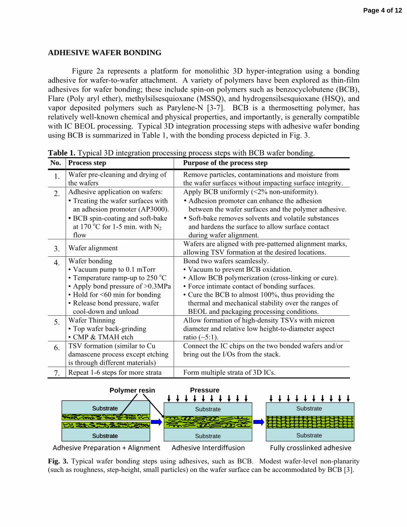
ADHESIVE WAFER BONDING
Figure 2a represents a platform for monolithic 3D hyper-integration using a bonding adhesive for wafer-to-wafer attachment. A variety of polymers have been explored as thin-film adhesives for wafer bonding; these include spin-on polymers such as benzocyclobutene (BCB), Flare (Poly aryl ether), methylsilsesquioxane (MSSQ), and hydrogensilsesquioxane (HSQ), and vapor deposited polymers such as Parylene-N [3-7]. BCB is a thermosetting polymer, has relatively well-known chemical and physical properties, and importantly, is generally compatible with IC BEOL processing. Typical 3D integration processing steps with adhesive wafer bonding using BCB is summarized in Table 1, with the bonding process depicted in Fig. 3. Table 1. Typical 3D integration processing process steps with BCB wafer bonding. No. Process step Purpose of the process step
1. Wafer pre-cleaning and drying of the wafers
Remove particles, contaminations and moisture from the wafer surfaces without impacting surface integrity.
2. Adhesive application on wafers: • Treating the wafer surfaces with
an adhesion promoter (AP3000). • BCB spin-coating and soft-bake
at 170 oC for 1-5 min. with N2 flow
Apply BCB uniformly (<2% non-uniformity). • Adhesion promoter can enhance the adhesion
between the wafer surfaces and the polymer adhesive.• Soft-bake removes solvents and volatile substances
and hardens the surface to allow surface contact during wafer alignment.
3. Wafer alignment Wafers are aligned with pre-patterned alignment marks, allowing TSV formation at the desired locations.
4. Wafer bonding • Vacuum pump to 0.1 mTorr • Temperature ramp-up to 250 oC • Apply bond pressure of >0.3MPa• Hold for <60 min for bonding • Release bond pressure, wafer
cool-down and unload
Bond two wafers seamlessly. • Vacuum to prevent BCB oxidation. • Allow BCB polymerization (cross-linking or cure). • Force intimate contact of bonding surfaces. • Cure the BCB to almost 100%, thus providing the
thermal and mechanical stability over the ranges of BEOL and packaging processing conditions.
5. Wafer Thinning • Top wafer back-grinding • CMP & TMAH etch
Allow formation of high-density TSVs with micron diameter and relative low height-to-diameter aspect ratio (~5:1).
6. TSV formation (similar to Cu damascene process except etching is through different materials)
Connect the IC chips on the two bonded wafers and/or bring out the I/Os from the stack.
7. Repeat 1-6 steps for more strata Form multiple strata of 3D ICs.
Adhesive Preparation + Alignment Adhesive Interdiffusion Fully crosslinked adhesive
Polymer resin
Substrate
Substrate
Substrate
Substrate
Substrate
Substrate
Substrate
Substrate
Pressure
Substrate
Substrate
Substrate
Substrate
Substrate
Substrate
Fig. 3. Typical wafer bonding steps using adhesives, such as BCB. Modest wafer-level non-planarity (such as roughness, step-height, small particles) on the wafer surface can be accommodated by BCB [3].
Page 4 of 12

Figure 4 presents some wafer bonding results using BCB [8-10]. With the thermal coefficient-of-expansion (TCE) matched glass wafer, the bonding uniformity and bonding integrity can be visually inspected through the glass wafer (Figs. 4a and 4b) [8-9]. Figure 5 presents some results for wafer bonding integrity using BCB [9-10] in terms of mechanical bond strength and electrical property preservation of the devices and circuits. Major research advances with BCB bonding are summarized as follows [5-11]:
• Free of voids, defects and structural damage; • Sufficient high bond strength with a critical adhesion energy in the order of 30 J/m2; • No degradation of electrical characteristics on wafers with Cu interconnect test structures and
wafers with CMOS SOI Cu/Low-k devices and circuits after double bonding/thinning; • Comparable sawing results to 2D IC wafer; • No degradation in bond strength after conventional die packaging reliability tests.
1 2 3 4Sample Type
Oxidized Si wafer
0.4 µm BCB
Cu/oxide interconnect wafer
2.6 µm BCB
Cu/porous low-kinterconnect wafer
2.6 µm BCB
Oxidized Si wafer2.6 µm BCB
0
10
20
30
40
Criti
cal A
dhes
ion
Ener
gy(J
/m2 )
1 2 3 4Sample Type
1 2 3 4Sample Type
Oxidized Si wafer
0.4 µm BCB
Cu/oxide interconnect wafer
2.6 µm BCB
Cu/porous low-kinterconnect wafer
2.6 µm BCB
Oxidized Si wafer2.6 µm BCB
0
10
20
30
40
Criti
cal A
dhes
ion
Ener
gy(J
/m2 )
9.2 10-12 9.4 10-12 9.6 10-12 9.8 10-12 1 10-11.01
.1
1
510203050
70809095
99
99.9
99.99Ring Oscillator Delay
Delay Before BondDelay After Bond
Delay (0.2E-12 seconds per division)
Pro
babi
lity
Dis
tribu
tion
(%)
9.2 10-12 9.4 10-12 9.6 10-12 9.8 10-12 1 10-11.01
.1
1
510203050
70809095
99
99.9
99.99Ring Oscillator Delay
Delay Before BondDelay After Bond
Delay (0.2E-12 seconds per division)
Pro
babi
lity
Dis
tribu
tion
(%)
(a) (b)
Fig. 5. Wafer bonding integrity results using BCB: (a) Bonding strength (critical adhesion energy) for oxide surface, Cu/oxide and Cu/low-k interconnect, showing sufficient strength of BCB bonding [9], (b) probability distribution of ring oscillator delay for a wafer SOI wafer with 130 nm CMOS devices/circuits and Cu/low-k interconnects (provided by Freescale Semiconductor) bonded with a Si wafer after two bonding and thinning processes [10].
BCB
Si
CMOS SOI
(a) (b) (c)
Fig. 4. Wafer bonding results using BCB: (a) PG&O glass 1737 bonded to prime Si with BCB [8], (b) a wafer with Cu/oxide interconnect structures (provided by SEMATECH) bonded to a TCE-matched glass wafer (Corning glass 7740) after removing the Si substrate by grinding, polishing and TMAH etching [9], and (c) a SEM cross-section of wafer SOI wafer with 130 nm CMOS devices/circuits and Cu/low-k interconnects (provided by Freescale Semiconductor) bonded with a Si wafer after two bonding and thinning processes [10].
Page 5 of 12

Three key advantages of this approach are: (1) the ability of the dielectric adhesive to accommodate wafer surface non-planarity (e.g., due to the last BEOL metallization) and particulates at the bonding interfaces; (2) no handling wafers are required, i.e., thinned silicon is not transferred as in some other wafer-level 3D approaches; and (3) stacks of three or more wafers can be fabricated without changing the processing approach since the wafer bond with fully-cured BCB sandwiched between two silicon wafers is thermally stable up to 400 oC [7]. METAL WAFER BONDING
Figure 2b represents a monolithic 3D hyper-integration platform using metal bonding for wafer-to-wafer attachment and interstrata vias. A few metals and metal alloys are reported for wafer bonding, such as Cu [12-17], InAu [25], CuSn [28]. However, Cu based wafer bonding has been extensively studied because Cu is the choice of interconnect material and the bonding process is compatible with BEOL processing. Table 2 represents the typical 3D integration processing steps with wafer bonding using Cu; Figure 6 illustrates the key Cu bonding steps. Table 2. Typical 3D integration processing process steps with Cu wafer bonding. No. Process step Purpose of the process step
1. Wafer pre-cleaning and drying of the wafers
Remove particles, contaminations and moisture from the wafer surfaces.
2. Metal bonding interface formation: • Cu/SiO2 damascene (CMP) • SiO2 recess and Cu surface
treatment
Form metal bonding pads, posts and “dummy” bonding surfaces. • CMP to form flat surface across the wafers. • Form a dome shape of Cu pads/posts and remove
copper oxide, allowing low resistance Cu bonds.
3. Wafer alignment Wafers are aligned with pre-patterned alignment marks, allowing Cu bonding at the desired locations.
4. Wafer bonding • Vacuum pump to 0.1 mTorr • Temperature ramp-up to 350 oC • Apply bond pressure of >0.3MPa• Hold for <60 min for bonding • Release bond pressure, wafer
cool-down and unload (optional further anneal)
Bond two wafers seamlessly at the metal interface. • Vacuum to prevent metal (Cu) oxidation. • Allow Cu interdiffusion across the interface. • Force intimate contact of bonding surfaces. • Allow Cu interdiffusion and grain growth across the
bonding interfaces, and eliminate small voids at the bonding interface. Optional anneal allows shorter bonding time in the bonding chamber.
5. Wafer Thinning • Top wafer back-grinding • CMP & TMAH etch
Allow formation of high-density TSVs with micrometer diameter and relative low height-to-diameter aspect ratio (~5:1).
6. TSV formation (similar to Cu damascene process)
Connect the IC chips in the stack to next stratum and/or bring out the I/Os from the stack.
7. Repeat 1-6 steps for more strata Form multiple strata of 3D ICs.
One of the key process steps is to remove the surface copper oxide right before the bonding process, using either wet chemicals such as a dilute-HCl dip for 30s or in-situ plasma etch [13]. Long bonding time and/or optional post-bond anneal improve the Cu bonding interface morphology and bonding integrity as shown in Figs. 7 and 8 [14-15]. The other key steps are the SiO2 recess and Cu surface shaping. The SiO2 recess allows Cu surfaces on two wafers can be contacted; while the surface profile control further improves
Page 6 of 12
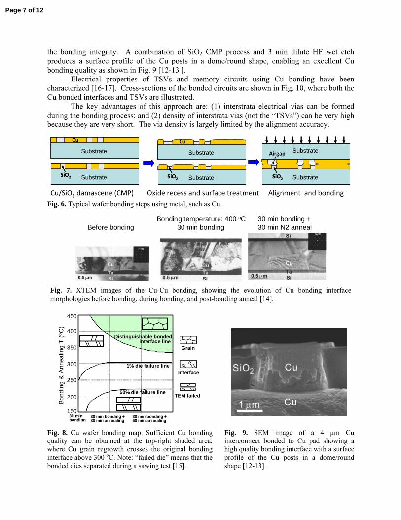
Before bonding 30 min bonding30 min bonding + 30 min N2 anneal
Bonding temperature: 400 oC
Fig. 7. XTEM images of the Cu-Cu bonding, showing the evolution of Cu bonding interfacemorphologies before bonding, during bonding, and post-bonding anneal [14].
the bonding integrity. A combination of SiO2 CMP process and 3 min dilute HF wet etch produces a surface profile of the Cu posts in a dome/round shape, enabling an excellent Cu bonding quality as shown in Fig. 9 [12-13 ].
Electrical properties of TSVs and memory circuits using Cu bonding have been characterized [16-17]. Cross-sections of the bonded circuits are shown in Fig. 10, where both the Cu bonded interfaces and TSVs are illustrated.
The key advantages of this approach are: (1) interstrata electrical vias can be formed during the bonding process; and (2) density of interstrata vias (not the “TSVs”) can be very high because they are very short. The via density is largely limited by the alignment accuracy.
Cu/SiO2 damascene (CMP)
Substrate
Substrate
Substrate
Substrate
Cu
Substrate
Substrate
Substrate
Substrate
Cu
SiO2SiO2
Oxide recess and surface treatment Alignment and bonding
SubstrateSubstrate
Substrate
SiO2SiO2 SiO2SiO2
Airgap
Fig. 6. Typical wafer bonding steps using metal, such as Cu.
Bon
ding
& A
nnea
ling
T (o C
)
Grain
Interface
TEM failed
450
400
350
250
150
300
200
30 min bonding +30 min annealing
30 min bonding +60 min annealing
30 min bonding
Distinguishable bondedinterface line
1% die failure line
50% die failure line
Fig. 8. Cu wafer bonding map. Sufficient Cu bondingquality can be obtained at the top-right shaded area,where Cu grain regrowth crosses the original bondinginterface above 300 oC. Note: “failed die” means that thebonded dies separated during a sawing test [15].
Fig. 9. SEM image of a 4 μm Cu interconnect bonded to Cu pad showing a high quality bonding interface with a surface profile of the Cu posts in a dome/round shape [12-13].
Page 7 of 12

SupercontactTM
SuperviasTM
(a) (b)
Fig. 10. Cross-sections of Cu bonding interfaces: (a) Intel 65nm strained Si Cu/low-k SRAM [16] and (b) Tezzaron memory stack [17]. Both show the Cu bonded vias (marked as “bonded structure” in the leftimage and “SuperviasTM” in the right image) and TSVs (marked as “SupercontactTM” in the left image).
One concern with Cu bonding is the airgap between the bonding interfaces as shown in Fig. 6, which could lead to potential reliability issues (e.g., chip sealing, Cu erosion, mechanical stress and delamination of the bonds). Bonded dummy Cu rings around the chip edge can provide a chip seal between the bonded chips, while bonded dummy Cu pads across the wafer can increase the thermal conductivity between the bonded chips as well as the bonding integrity (such as reducing the failure of die sawing [12, 15]). These potential reliability concerns could be further reduced with the metal/adhesive wafer bonding as discussed in the next section. METAL/ADHESIVE WAFER BONDING
Figure 2c represents a monolithic 3D hyper-integration platform, which employs wafer bonding of damascene-patterned metal/adhesive redistribution layers on two wafers for wafer-to-wafer attachment and interstrata vias. This platform combines the advantages of the adhesive bonding and metal bonding, in particular, the BCB bond robustness and direct interstrata electrical vias of Cu bonds [18-22]. Table 3 represents the typical 3D integration processing steps with wafer bonding using damascene-patterned metal/adhesive redistribution layers; Figure 11 illustrates the key steps of Cu/BCB wafer bonding. The key challenges with this metal/adhesive bonding include (1) selection of metals and adhesives for damascene patterning and (2) wafer-level feature-scale planarization (CMP) to ensure bonding integrity and low resistance of electrical interstrata vias. A Cu/BCB system was selected to demonstrate this bonding approach, where BCB was partially cured to enable the Cu/BCB CMP [20] as described in Table 3. Figure 12 shows that intimate contacts can be achieved at Cu-to-Cu, BCB-to-BCB and Cu-to-BCB interfaces; while further processing optimization is needed to eliminate the small voids at the bonding interface [18-19]. Mechanical characterization on bonded wafers using partially-cured BCB shows sufficient bond strength (in a range of 15-30 J/m2, depending on the processing conditions [18]). Figure 13a shows a bond strength of the partially-cured BCB is close to 32 J/m2 as found when using soft-baked BCB [7, 21]. For electrical characterization, a via-chain structure was fabricated with electrical testing probes shown in Fig. 13b. The contact resistance was on the order of 1x10⁻⁷ Ω-cm2 [18]. These results are quite promising, and demonstrate the feasibility of this 3D technology platform.
Page 8 of 12

Table 3. Typical 3D integration processing process steps with Cu/BCB wafer bonding. No. Process step Purpose of the process step
1. Wafer pre-cleaning and drying of the wafers
Remove particles, contaminations and moisture from the wafer surfaces.
2. Adhesive application on wafers: • Treating the wafer surfaces with
an adhesion promoter (AP3000). • BCB spin-coating and soft-bake
at 170 oC for 1-5 min. with N2 flow
• Partial cure of BCB at 250oC for 60 seconds or more
Apply BCB uniformly (<2% non-uniformity). • Adhesion promoter can enhance the adhesion
between the wafer surfaces and the polymer adhesive.• Soft-bake removes solvents and volatile substances
and hardens the surface to allow surface contact during wafer alignment
• Partial cure results in >55% BCB crosslinking, enabling Cu/BCB CMP process [20].
3. Metal/adhesive bonding interface formation: • Cu/BCB damascene (CMP)
Form metal bonding pads, posts and “dummy” bonding surfaces. • CMP to form flat surface across the wafers.
4. Wafer alignment Wafers are aligned with pre-patterned alignment marks, allowing TSV formation at the desired locations.
5. Wafer bonding • Vacuum pump to 0.1 mTorr • Temperature ramp-up to 250 oC • Apply bond pressure of >0.3MPa• Hold for <60 min for bonding • Temperature ramp-up to 350 oC • Hold for <60 min for bonding • Release bond pressure, wafer
cool-down and unload (optional further anneal)
Bond two wafers seamlessly. • Vacuum to prevent oxidation of metal and adhesives. • Allow BCB polymerization (cross-linking or cure). • Force intimate contact of bonding surfaces. • Cure the BCB to almost 100%. • Allow Cu interdiffusion and grain growth across the
bonding interfaces, and eliminate small voids at the bonding interface. Optional anneal allows shorter bonding time in the bonding chamber.
6. Wafer Thinning • Top wafer back-grinding • CMP & TMAH etch
Allow formation of high-density TSVs with micrometer diameter and relative low height-to-diameter aspect ratio (~5:1).
7. TSV formation (similar to Cu damascene process)
Connect the IC chips in the stack to next stratum and/or bring out the I/Os from the stack.
8. Repeat 1-7 steps for more strata Form multiple strata of 3D ICs.
The overall key advantages of this platform include (1) both electrical and mechanical inter-wafer connections/bonds (i.e., high-density Cu/Cu bonded vias and robust BCB/BCB bonds) formed in one unit processing step; and (2) redistribution layers for inter-wafer interconnect routing for wafers, on which the inter-wafer interconnect pads are not matched, which further reduces the process flow and allows larger alignment tolerance.
Cu/BCB damascene (CMP)
Substrate
Substrate
Substrate
SubstrateBCB
Cu
Alignment and BCB bonding Cu bonding
SubstrateSubstrate
Substrate
SubstrateSubstrate
Substrate
BCB Cu
Fig. 11. Typical wafer bonding steps using metal/adhesive, such as Cu/BCB.
Page 9 of 12

DISCUSSION AND CONCLUSIONS
Based on the 3D technology developments so far, the key advantage of the 3D approach using adhesive bonding is that the wafer bonding process is separated from interstrata via formation. Therefore, a robust mechanical/chemical wafer bond, for instance, using BCB, can be easily achieved compared to other 3D approaches. The key concern is that the TSV density could be relatively low because of the large via diameter required for long TSVs to pass through the thinned silicon substrate, particularly if a bulk silicon wafer is used [16-17]. If an silicon-on-isolator (SOI) wafer is used for the top wafer, a high density of short TSVs can also be achieved using BEOL damascene patterning process through the buried oxide (BOX)/SOI layer because the bulk silicon substrate of the SOI wafer can be completely removed [8], leaving only the BOX/SOI layer with a thickness of a few ten to a few hundred nanometers [10-11]. In fact, these TSVs are formed through the SiO2 layer surrounding the SOI CMOS device islands; there is no
Displacement (mm) 20 40 60 80 1000 80
10
20
30
0
Load
(N)
0.00 0.02 0.04 0.06 0.08 0.10 0.12
Pc
(a) (b) Fig. 13. (a) Load-displacement characteristics of typical partially-cured BCB bonding interface tested by four-point bending technique, showing strong bonding strength (~30 J/mm2 calculated from this plot) [18, 21]; (b) image of a via-chain structure with electrical testing probes [18, 21].
Bottom wafer
0.2 µm
BCB
BCB Cu
Ta (Cu liner)
Bonding interface
Top wafer
Bottom wafer0.2 µm
BCB
BCB Cu
Ta (Cu liner)
Bonding interface
Top wafer
Bottom wafer
Bonding condition:250oC for 60 min. + 350oC for 60 min.
Top wafer
Cu
Cu
1 µm
BCB
BCB
Cu void filled Top wafer
Cu
Cu
1 µm
BCB
BCB
Cu void filled
Fig. 12. Cross-sectional FIB/SEM image of bonded damascene patterned Cu/BCB wafers showingwell bonded Cu-to-Cu, BCB-to-BCB interfaces with a two bonding temperature levels of 250 oC and 350 oC for BCB and Cu bonding, respectively [18-19].
Page 10 of 12

silicon layer for TSVs to go through. Therefore, the term “TSVs” is defined as “through-strata-vias” in this paper.
The key advantage of the 3D approaches using metal or metal/adhesive bonding is that a high density of interstrata vias can be formed at the bonding interface. For metal/adhesive bonding, an additional key advantage is that the formation of bond vias and wafer bonding are done in one unit process, offering the combined process integration advantages of metal-to-metal electrical bonding (e.g., Cu-to-Cu) with the increased adhesion strength and robustness of dielectric adhesive bonding (e.g., using partially-cured BCB). However, if the top wafers are bulk silicon wafers, the density of TSVs, which interconnect the bonded wafers to the next top stratum and/or bring out the I/Os from the stack as shown in Fig. 10, is comparable to that with the adhesive bonding 3D platform because TSVs will need to be routed through a similar thickness of silicon. Similarly, a SOI wafer is a better choice as the top wafer for TSV formation in these 3D platforms. Though the use of SOI wafers obviously makes the wafer thinning and TSV formation much easier, hence low-cost for TSVs, the choice to use SOI or bulk silicon wafer depends on overall processing protocols, components in the system, and IC manufacturer preferences. Further research and development is necessary to fully evaluate these platforms. ACKNOWLEDGMENTS This research has been supported by the Interconnect Focus Center (IFC), NYSTAR, and DARPA (through IBM). The IFC is one of five research centers funded under the Focus Center Research Program, a Semiconductor Research Corporation and DARPA program. REFERENCES [1] J.-Q. Lu, “3D Hyper-Integration and Packaging Technologies for Micro-Nano-Systems,” Proceedings of The
IEEE, Vol. 97, No. 1, January 2009. [2] P. Garrou, P. Ramm, and C. Bower, editors, Handbook of 3D Integration: Technology and Applications of 3D
Integrated Circuits, Wiley-VCN, May 2008. [3] J.-Q. Lu, T.S. Cale and R.J. Gutmann, “3D Integration Based upon Dielectric Adhesive Bonding”, in Wafer
Level 3-D ICs Process Technology, eds., C.S. Tan, R.J. Gutmann, and R. Reif, pp. 219-256, Springer, 2008. [4] F. Niklaus, G. Stemme, J.-Q. Lu, and R. Gutmann, “Adhesive Wafer Bonding,” Journal of Applied Physics
(Applied Physics Review – Focused Review), Vol. 99, Issue 3, pp. 031101-1-28, Feb. 1, 2006. [5] J.-Q. Lu, Y. Kwon, R.P. Kraft, R.J. Gutmann, J.F. McDonald, and T.S. Cale, “Stacked Chip-to-Chip
Interconnections Using Wafer Bonding Technology with Dielectric Bonding Glues,” 2001 IEEE International Interconnect Technology Conference (IITC 2001), pp. 219-221, IEEE, June 4 - 6, 2001.
[6] J.-Q. Lu, T.S. Cale, and R.J. Gutmann, “Wafer-Level Three-Dimensional Hyper-Integration Technology Using Dielectric Adhesive Wafer Bonding,” Materials for Information Technology: Devices, Interconnects and Packaging, eds., E. Zschech, C. Whelan, T. Mikolajick, pp. 386 – 397, Springer-Verlag, August 2005.
[7] Y. Kwon, J. Seok, J.-Q. Lu, T.S. Cale and R.J. Gutmann, “Critical Adhesion Energy of Benzocyclobutene (BCB)-Bonded Wafers,” Journal of The Electrochemical Society, 153 (4), pp. G347-G352 (2006).
[8] J.-Q. Lu, K.W. Lee, Y. Kwon, G. Rajagopalan, J. McMahon, B. Altemus, M. Gupta, E. Eisenbraun, B. Xu, A. Jindal, R.P. Kraft, J.F. McDonald, J. Castracane, T.S. Cale, A. Kaloyeros, and R.J. Gutmann, “Processing of Inter-Wafer Vertical Interconnects in 3D ICs,” Advanced Metallization Conference in 2002 (AMC 2002), pp. 45-51, eds., B.M. Melnick, T.S. Cale, S. Zaima, and T. Ohta, MRS Proc. Vol. V18. 2003.
[9] J.-Q. Lu, A. Jindal, Y. Kwon, J.J. McMahon, M. Rasco, R. Augur, T.S. Cale, and R.J. Gutmann, “Evaluation Procedures for Wafer Bonding and Thinning of Interconnect Test Structures for 3D ICs,” 2003 IEEE International Interconnect Technology Conference (IITC 2003), pp. 74-76, June 2003.
[10] R.J. Gutmann, J.-Q. Lu, S. Pozder, Y. Kwon, D. Menke, A. Jindal, M. Celik, M. Rasco, J.J. McMahon, K. Yu, and T.S. Cale, “A Wafer-Level 3D IC Technology Platform,” Advanced Metallization Conference in 2003 (AMC 2003), pp. 19-26, 2003.
Page 11 of 12

[11] S. Pozder, J.-Q. Lu, Y. Kwon, S. Zollner, J. Yu, J.J. McMahon, T.S. Cale, K. Yu, and R.J. Gutmann, “Back-End Compatibility of Bonding and Thinning Processes for a Wafer-Level 3D Interconnect Technology Platform,” IEEE International Interconnect Technology Conference (IITC 2004), pp. 102-104, June 2004.
[12] K.-N. Chen, S.H. Lee, P.S. Andry, C.K. Tsang, A.W. Topol, Y.-M. Lin, J.-Q. Lu, A.M.Young, M. Ieong, and W. Haensch, “Structure Design and Process Control for Cu Bonded Interconnects in 3D Integrated Circuits,” Technical Digest of IEEE International Electron Devices Meeting (2006 IEDM), pp 367-370, Dec. 2006.
[13] K.N. Chen, C.K. Tsang, A.W. Topol, S.H. Lee, B.K. Furman, D.L. Rath, J.-Q. Lu, A.M. Young, S. Purushothaman, and W. Haensch, “Improved Manufacturability of Cu Bond Pads and Implementation of Seal Design in 3D Integrated Circuits and Packages”, in 23rd International VLSI Multilevel Interconnection (VMIC) Conference, ed., T. Wade, pp. 195-202, IMIC, September 2006.
[14] K. N. Chen, A. Fan, C. S. Tan, and R. Reif, “Microstructure Evolution and Abnormal Grain Growth during Copper Wafer Bonding,” Applied Physics Letters, Vol. 81, No. 20, pp. 3774-3776, 2002.
[15] K.N. Chen, C.S. Tan, A. Fan and R. Reif, “Morphology and Bond Strength of Copper Wafer Bonding”, Electrochemical and Solid-State Letters, 7(1), pp G14-G16, 2004.
[16] P. Morrow, C.-M. Park, S. Ramanathan, M. J. Kobrinsky, and M. Harmes, “Three-Dimensional Wafer Stacking Via Cu-Cu Bonding integrated With 65-nm Strained-Si/Low-k CMOS Technology,” IEEE Electron Device Letters, Vol. 27, No. 5, pp. 335-337, 2006.
[17] R. Patti, “Three-Dimensional Integrated Circuits and the Future of System-on-Chip Designs,” Proceedings of The IEEE, Vol. 94, No. 6, pp. 1214-1222, 2006.
[18] J.J. McMahon, J.-Q. Lu, and R. J. Gutmann, “Wafer Bonding of Damascene-Patterned Metal/Adhesive Redistribution Layers for Via-First 3D Interconnect,” 55th IEEE Electronic Components and Technology Conference (ECTC 2005), pp. 331-336, 2005.
[19] J.-Q. Lu, J.J. McMahon, and R.J. Gutmann, “Via-First Inter-Wafer Vertical Interconnects utilizing Wafer-Bonding of Damascene-Patterned Metal/Adhesive Redistribution Layers,” 3D Packaging Workshop at IMAPS Device Packaging Conference, Scottsdale, AZ, March 20-23, 2006.
[20] J. J. McMahon, F. Niklaus, R. J. Kumar, J. Yu, J.-Q. Lu, and R. J. Gutmann, “CMP Compatibility of Partially Cured Benzocyclobutene (BCB) for a Via-First 3D IC Process”, in Chemical-Mechanical Planarization—Integration, Technology and Reliability, eds., A. Kumar, J.A. Lee, Y.S. Obeng, I. Vos, E.C. Johns, MRS Proceedings Vol. 867, pp. W4.4.1-6, Spring 2005.
[21] R.J. Gutmann, J.J. McMahon, and J.-Q. Lu, “Damascene Patterned Metal/Adhesive Redistribution Layers,” in Enabling Technologies for 3-D Integration, eds., C.A. Bower, P.E. Garrou, P. Ramm, and K. Takahashi MRS Proceedings Vol. 970, paper #, 0970-Y04-02, 2006.
[22] J.J. McMahon, E. Chan, S.H. Lee, R.J. Gutmann, and J.-Q. Lu, “Bonding Interfaces in Wafer-Level Metal/Adhesive Bonded 3D Integration”, in The 58th Electronic Components and Technology Conference (ECTC 2008), pp. 871-878, May 2008.
[23] K.W. Guarini, A.W. Topol, M. Ieong, R. Yu, L. Shi, M.R. Newport, D.J. Frank, D.V. Singh, G.M. Cohen, S.V. Nitta, D.C. Boyd, P.A. O’Neil, S.L. Tempest, H.B. Pogge, S. Purushothaman, and W.E. Haensch, “Electrical Integrity of State-of-the-Art 0.13 mm SOI CMOS Devices and Circuits Transferred for Three-Dimensional (3D) Integrated Circuit (IC) Fabrication,” Technical Digest of IEEE International Electron Devices Meeting (2002 IEDM), pp. 943-945, 2002.
[24] J.A. Burns, B.F. Aull, C.K. Chen, C.-L. Chen, C.L. Keast, J.M. Knecht, V. Suntharalingam, K. Warner, P.W. Wyatt, and D.-R.W. Yost, “A Wafer-Scale 3-D Circuit Integration Technology,” IEEE Trans. Electron Devices, Vol. 53, No. 10, pp. 2507-2516, October 2006.
[25] K.W. Lee, T. Nakamura, T. One, Y. Yamada, T. Mizukusa, H. Hasimoto, K.T. Park, H. Kurino, and M. Koyanagi, “Three Dimensional Shared Memory Fabricated Using Wafer Stacking Technology,” Technical Digest of IEEE International Electron Devices Meeting (2000 IEDM), pp. 165-168, 2000.
[26] K. Gann, “Neo-Stacking Technology,” High Density Interconnect Magazine, Vol. 2, December, 1999. [27] J.U. Knickerbocker, P.S. Andry, LP. Buchwalter, E.G. Colgan, J. Cotte, H. Gan, R.R. Horton, S.M. Sri-
Jayantha, J H. Magerlein, D. Manzer, G. McVicker, C S. Patel, R.J. Polastre, E.S. Sprogis, C.K. Tsang, B.C. Webb, and S.L. Wright, “System-on-Package (SOP) Technology, Characterization and Applications,” 56th IEEE Electronic Components and Technology Conference (ECTC 2006), pp. 415-421, 2006.
[28] R. Wieland, D. Bonfert, A. Klumpp, R. Merkel, L. Nebrich, J. Weber, and P. Ramm, “3D Integration of CMOS transistors with ICV-SLID technology,” Microelectronic Engineering, Vol. 82, p. 529-33, 2005.
Page 12 of 12


![EUROPEAN ADHESIVE ENGINEERadtecheducation.com/documents/results/3.Training...Handbook of Adhesive Technology, Marcel Dekker, 2003 [4] Dissimilar Metal Joining Technologies for Steel](https://static.fdocuments.in/doc/165x107/5f1843a4accca4036638d98e/european-adhesive-eng-handbook-of-adhesive-technology-marcel-dekker-2003-4.jpg)