11/01/05ELEC 5970-001/6970-001 Lecture 171 ELEC 5970-001/6970-001(Fall 2005) Special Topics in...
22
11/01/05 ELEC 5970-001/6970-001 Lectur e 17 1 ELEC 5970-001/6970-001(Fall 2005) Special Topics in Electrical Engineering Low-Power Design of Electronic Circuits Low-Power Logic Design and Parallelism Vishwani D. Agrawal James J. Danaher Professor Department of Electrical and Computer Engineering Auburn University http://www.eng.auburn.edu/~vagrawal [email protected]
-
date post
19-Dec-2015 -
Category
Documents
-
view
227 -
download
1
Transcript of 11/01/05ELEC 5970-001/6970-001 Lecture 171 ELEC 5970-001/6970-001(Fall 2005) Special Topics in...

11/01/05 ELEC 5970-001/6970-001 Lecture 17 1
ELEC 5970-001/6970-001(Fall 2005)Special Topics in Electrical EngineeringLow-Power Design of Electronic Circuits
Low-Power Logic Designand Parallelism
Vishwani D. AgrawalJames J. Danaher Professor
Department of Electrical and Computer EngineeringAuburn University
http://www.eng.auburn.edu/[email protected]

11/01/05 ELEC 5970-001/6970-001 Lecture 17 2
State Encoding• Two-bit binary counter:
• State sequence, 00→01→10→11→00• Six bit transitions in four clock cycles• 6/4 = 1.5 transitions per clock
• Two-bit Gray-code counter• State sequence, 00→01→11→10→00• Four bit transitions in four clock cycles• 4/4 = 1.0 transition per clock
• Gray-code counter is more power efficient.
G. K. Yeap, Practical Low Power Digital VLSI Design, Boston:Kluwer Academic Publishers (now Springer), 1998.

11/01/05 ELEC 5970-001/6970-001 Lecture 17 3
Three-Bit CountersBinary Gray-code
State No. of toggles State No. of toggles
000 - 000 -
001 1 001 1
010 2 011 1
011 1 010 1
100 3 110 1
101 1 111 1
110 2 101 1
111 1 100 1
000 3 000 1

11/01/05 ELEC 5970-001/6970-001 Lecture 17 4
N-Bit Counter: Toggles in Counting Cycle
• Binary counter: T(binary) = 2(2N – 1)• Gray-code counter: T(gray) = 2N
• T(gray)/T(binary) = 2N-1/(2N – 1) → 0.5
Bits T(binary) T(gray) T(gray)/T(binary)
1 2 2 1.0
2 6 4 0.6667
3 14 8 0.5714
4 30 16 0.5333
5 62 32 0.5161
6 126 64 0.5079
∞ - - 0.5000

11/01/05 ELEC 5970-001/6970-001 Lecture 17 5
Bus Encoding• Example: Four bit bus
• 0000→1110 has three transitions.• If bits of second pattern are inverted, then 0000→0001 will
have only one transition.
• Bit-inversion encoding for N-bit bus:
Number of bit transitions0 N/2 N
N
N/2
0Nu
mb
er
of b
it tr
an
sitio
ns
afte
r in
vers
ion
en
cod
ing

11/01/05 ELEC 5970-001/6970-001 Lecture 17 6
Bus-Inversion Encoding Logic
Polarity decision
logic
Se
nt d
ata
Re
ceiv
ed
da
ta
Bus register
Polarity bit
M. Stan and W. Burleson, “Bus-InvertCoding for Low Power I/O,” IEEE Trans.VLSI Systems, vol. 3, no. 1, pp. 49-58,March 1995.

11/01/05 ELEC 5970-001/6970-001 Lecture 17 7
FSM State Encoding
11
01000.1
0.10.4
0.3
0.6 0.9
0.6
01
11000.1
0.10.4
0.3
0.6 0.9
0.6
Expected number of state-bit transitions:
2(0.3+0.4) + 1(0.1+0.1) = 1.6 1(0.3+0.4+0.1) + 2(0.1) = 1.0
Transition probability based on
PI statistics
State encoding can be selected using a power-based cost function.

11/01/05 ELEC 5970-001/6970-001 Lecture 17 8
FSM: Clock-Gating• Moore machine: Outputs depend only on
the state variables.– If a state has a self-loop in the state transition
graph (STG), then clock can be stopped whenever a self-loop is to be executed.
Sj
SiSk
Xi/Zk
Xk/Zk
Xj/Zk
Clock can be stopped when (Xk, Sk) combination occurs.
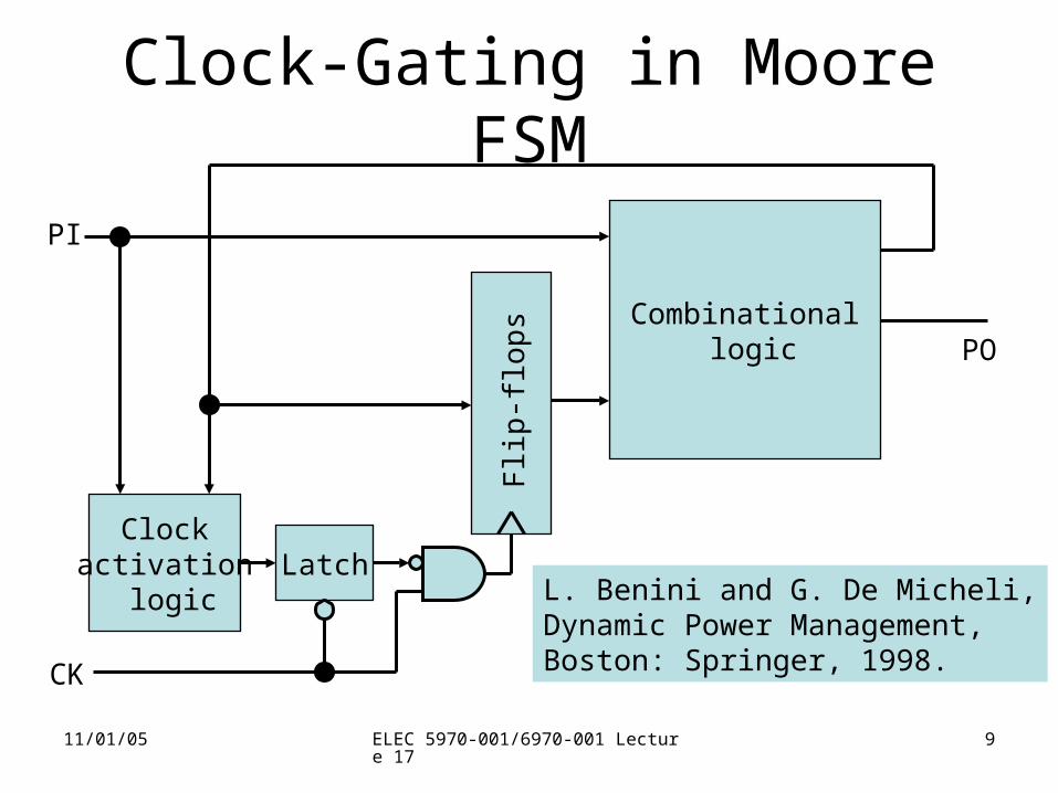
11/01/05 ELEC 5970-001/6970-001 Lecture 17 9
Clock-Gating in Moore FSM
Combinational logic
LatchClock
activation logic
Flip
-flo
ps
PI
CK
PO
L. Benini and G. De Micheli,Dynamic Power Management,Boston: Springer, 1998.
11/01/05 ELEC 5970-001/6970-001 Lecture 17 10
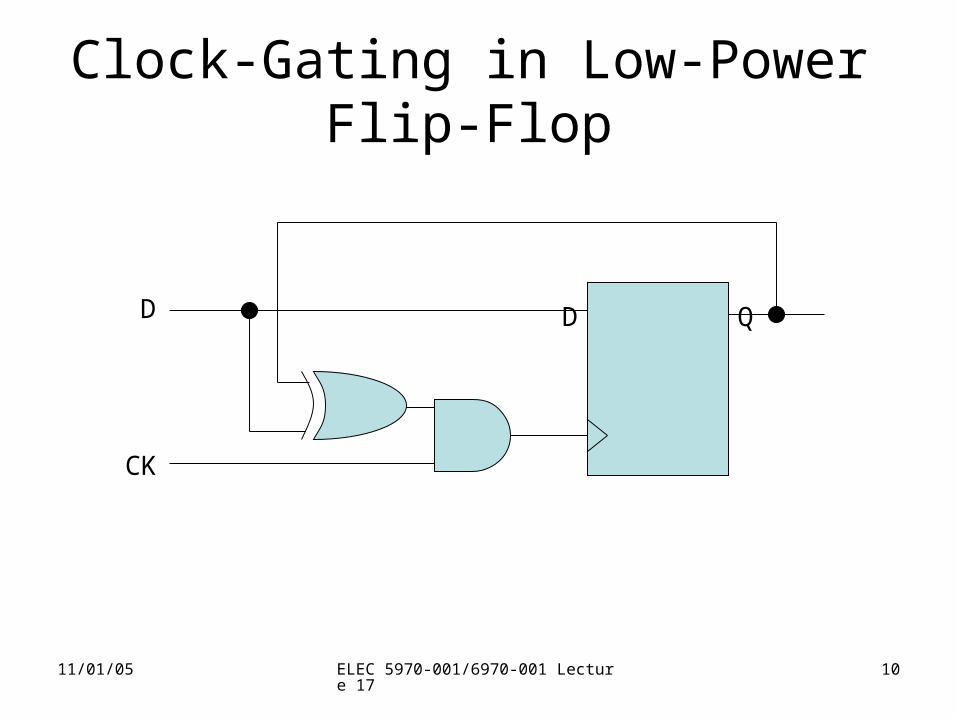
Clock-Gating in Low-Power Flip-Flop
D QD
CK

11/01/05 ELEC 5970-001/6970-001 Lecture 17 11
Low-Power Datapath Architecture• Lower supply voltage
– This slows down circuit speed– Use parallel computing to gain the speed back
• Works well when threshold voltage is also lowered.
• About 60% reduction in power obtainable.• Reference: A. P. Chandrakasan and R. W.
Brodersen, Low Power Digital CMOS Design, Boston: Kluwer Academic Publishers (Now Springer), 1995.

11/01/05 ELEC 5970-001/6970-001 Lecture 17 12
A Reference Datapath
Combinationallogic
OutputInputR
eg
iste
r
Re
gis
ter
CK
Supply voltage = Vref
Total capacitance switched per cycle = Cref
Clock frequency = fPower consumption: Pref = CrefVref
2f
Cref
11/01/05 ELEC 5970-001/6970-001 Lecture 17 13
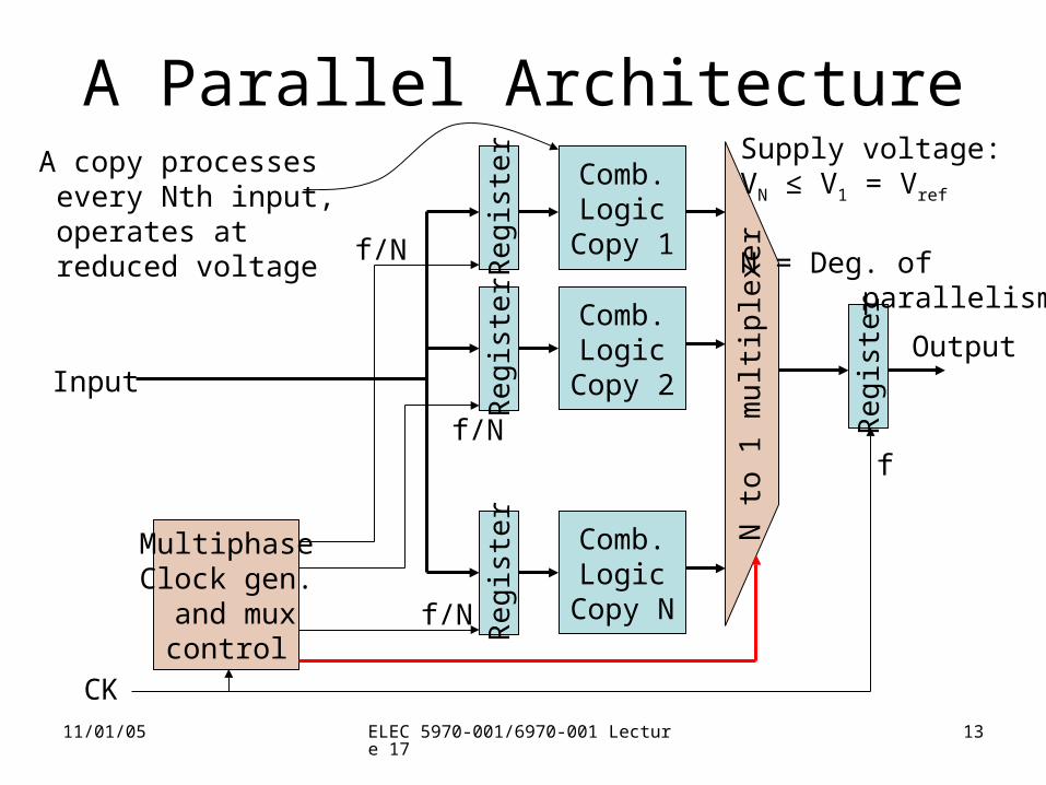
A Parallel ArchitectureComb.Logic
Copy 1
Comb.Logic
Copy 2
Comb.Logic
Copy N
Re
gis
ter
Re
gis
ter
Re
gis
ter
Re
gis
ter
N to
1 m
ulti
ple
xer
MultiphaseClock gen. and mux
control
InputOutput
CK
f
f/N
f/N
f/N
A copy processes every Nth input, operates at reduced voltage
Supply voltage:VN ≤ V1 = Vref
N = Deg. of parallelism
11/01/05 ELEC 5970-001/6970-001 Lecture 17 14
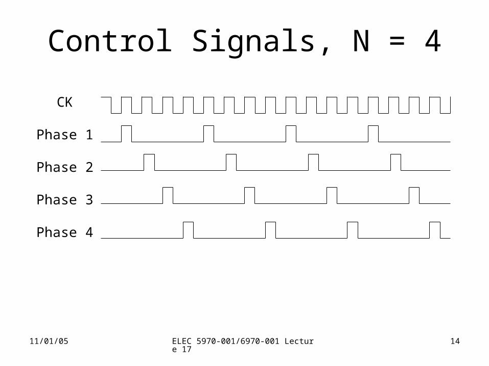
Control Signals, N = 4
CK
Phase 1
Phase 2
Phase 3
Phase 4
11/01/05 ELEC 5970-001/6970-001 Lecture 17 15
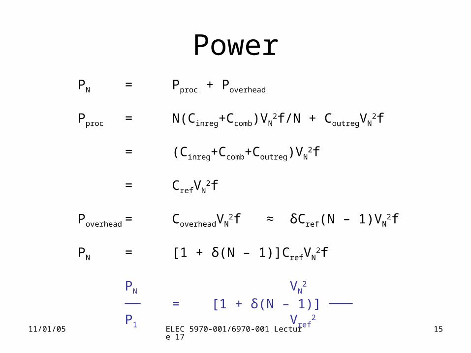
PowerPN = Pproc + Poverhead
Pproc = N(Cinreg+Ccomb)VN2f/N + CoutregVN
2f
= (Cinreg+Ccomb+Coutreg)VN2f
= CrefVN2f
Poverhead = CoverheadVN2f ≈ δCref(N – 1)VN
2f
PN = [1 + δ(N – 1)]CrefVN2f
PN VN2
── = [1 + δ(N – 1)] ───P1 Vref
2

11/01/05 ELEC 5970-001/6970-001 Lecture 17 16
Voltage vs. Speed CLVref CLVref
Delay of a gate, T ≈ ──── = ────────── I k(W/L)(Vref – Vt)2
where I is saturation currentk is a technology parameterW/L is width to length ratio of transistorVt is threshold voltage
Supply voltage
No
rma
lize
d g
ate
de
lay,
T
4.0
3.0
2.0
1.0
0.0 Vt Vref =5VV2=2.9V
N=1
N=2
V3
N=31.2μ CMOS Voltage reduction
slows down as we get closer to Vt

11/01/05 ELEC 5970-001/6970-001 Lecture 17 17
Increasing Multiprocessing
PN/P1
1 2 3 4 5 6 7 8 9 10 11 12
1.0
0.8
0.6
0.4
0.2
0.0
Vt=0V (extreme case)
Vt=0.4V
Vt=0.8V
N
1.2μ CMOS, Vref = 5V

11/01/05 ELEC 5970-001/6970-001 Lecture 17 18
Extreme Case: Vt = 0Delay, T α 1/ Vref
For N processing elements, delay = NT → VN = Vref/N
PN 1── = [1+ δ (N – 1)] ── → 1/NP1 N2
For negligible overhead, δ→0
PN 1── ≈ ──P1 N2
For Vt > 0, power reduction is less and there will be an optimum value of N.

11/01/05 ELEC 5970-001/6970-001 Lecture 17 19
Reduced-Power Shift Register
D Q D Q D Q
D QD QD Q
D Q
D Q
D
CK(f/2)
mu
ltip
lexe
r
Output
Flip-flops are operated at full voltage and half the clock frequency.

11/01/05 ELEC 5970-001/6970-001 Lecture 17 20
Power Consumption of Shift Reg.P = C’VDD
2f/n
Degree of parallelism, n1 2 4
No
rma
lize
d p
ow
er
1.0
0.5
0.25
0.0
Deg. Of parallelism
Freq (MHz)
Power (μW)
1 33.0 1535
2 16.5 887
4 8.25 738
16-bit shift register, 2μ CMOS
C. Piguet, “Circuit and Logic LevelDesign,” pages 103-133 in W. Nebeland J. Mermet (ed.), Low PowerDesign in Deep SubmicronElectronics, Boston: Kluwer Academic Publishers, 1997.

11/01/05 ELEC 5970-001/6970-001 Lecture 17 21
Multicore Processors
• D. Geer, “Chip Makers Turn to Multicore Processors,” Computer, vol. 38, no. 5, pp. 11-13, May 2005.
• A. Jerraya, H. Tenhunen and W. Wolf, “Multiprocessor Systems-on-Chips,” Computer, vol. 5, no. 7, pp. 36-40, July 2005; this special issue contains three more articles on multicore processors.

11/01/05 ELEC 5970-001/6970-001 Lecture 17 22
Multicore Processors
2000 2004 2008
Per
form
ance
bas
ed o
nS
PE
Cin
t200
0 an
d S
PE
Cfp
2000
ben
chm
arks
Multicore
Single core
Computer, May 2005, p. 12