University of Pavia - IRIS UNIPV
109
University of Pavia Ph.D. Thesis in Microelectronics XXXII Cycle Supervisor: Prof. Andrea Mazzanti Coordinator: Prof. Piero Malcovati Author: Hongyang Zhang CMOS Continuous-Time Linear Equalizers for High-Speed Serial Links
Transcript of University of Pavia - IRIS UNIPV
University of Pavia
Ph.D. Thesis in Microelectronics
XXXII Cycle
Supervisor:
Prof. Andrea Mazzanti
Coordinator:
Prof. Piero Malcovati
Author:
Hongyang Zhang
CMOS Continuous-Time Linear Equalizers
for High-Speed Serial Links
CMOS Continuous-Time Linear Equalizers
for High-Speed Serial Links

i

ii
Table of Contents
Table of Contents .................................................................................................... ii
List of Figures ........................................................................................................... v
List of Tables .......................................................................................................... ix
List of Acronyms ...................................................................................................... x
Abstract ..................................................................................................................... 1
Chapter 1 Introduction ............................................................................................ 3
Chapter 2 Background of wireline communications ............................................ 9
2.1 Wireline communication signaling.......................................................................................9
2.1.1 NRZ Modulation ...............................................................................................9
2.1.2 PAM-4 Modulation .........................................................................................11
2.2 Signal quality ......................................................................................................................13
2.2.1 Inter-symbol interference (ISI) .......................................................................13
2.2.2 Jitter ................................................................................................................14
2.2.3 Measurements of signal quality ......................................................................16
2.3 Channel characteristics .......................................................................................................20
2.3.1 Frequency-dependent impairments .................................................................22
2.3.2 Reflections ......................................................................................................26
2.3.3 Crosstalk .........................................................................................................29
Chapter 3 Analog equalization techniques ..........................................................32
3.1 Introduction ........................................................................................................................32
3.2 CTLE operation and evolution ...........................................................................................33
3.2.1 One-stage equalizer ........................................................................................34
3.2.2 Cascaded equalizer .........................................................................................36
iii
3.2.3 Low frequency equalizer ................................................................................38
3.2.4 Split-path equalizer .........................................................................................40
3.3 Broadband techniques ........................................................................................................42
3.3.1 Inductive peaking ............................................................................................42
3.3.2 Negative capacitance ......................................................................................45
3.4 Equalizer adaptation overview ...........................................................................................46
Chapter 4 Flexible transversal continuous-time linear equalizer operating up
to 25Gb/s in 28nm CMOS .....................................................................................49
4.1 Introduction ........................................................................................................................49
4.2 Equalizer architecture and design .......................................................................................51
4.3 Equalizer circuits design ....................................................................................................53
4.4 Experimental results ...........................................................................................................56
Chapter 5 PAM-4 analog front-end for 64Gb/s transceiver in 28nm CMOS
FDSOI......................................................................................................................62
5.1 Introduction ........................................................................................................................62
5.2 Analog front-end architecture ............................................................................................65
5.3 Analog front-end circuits ....................................................................................................67
5.3.1 Variable gain amplifiers .................................................................................67
5.3.2 Continuous-time linear equalizer ....................................................................70
5.4 Experimental results ...........................................................................................................73
5.5 Conclusions ........................................................................................................................76
Chapter 6 PAM-4 analog front-end for 112Gb/s receiver in 7nm FinFet ........78
6.1 Introduction ........................................................................................................................78
6.2 Analog front-end architecture ............................................................................................80
6.3 CTLE circuits design for the analog-front-end ..................................................................81
6.4 Simulation results ...............................................................................................................85
6.5 Conclusions and future work ..............................................................................................87
Chapter 7 Conclusions and future work..............................................................89

iv
7.1 Summary ............................................................................................................................89
7.2 Future work ........................................................................................................................90
References: ..............................................................................................................91
Appendix .................................................................................................................96
List of publications: ..................................................................................................................96
v
List of Figures
Figure 1.1 Interconnections of servers in data center ..................................................................... 3
Figure 1.2 Global network IP traffic ............................................................................................... 4
Figure 1.3 Serial link standards ...................................................................................................... 4
Figure 1.4 Speeds of serial links in literature ................................................................................. 5
Figure 1.5 Backplanes inside a server............................................................................................. 6
Figure 1.6 Serial link transceiver prototype .................................................................................... 7
Figure 2.1 NRZ signals ................................................................................................................... 9
Figure 2.2 NRZ sequence 𝑥(𝑡) ....................................................................................................... 9
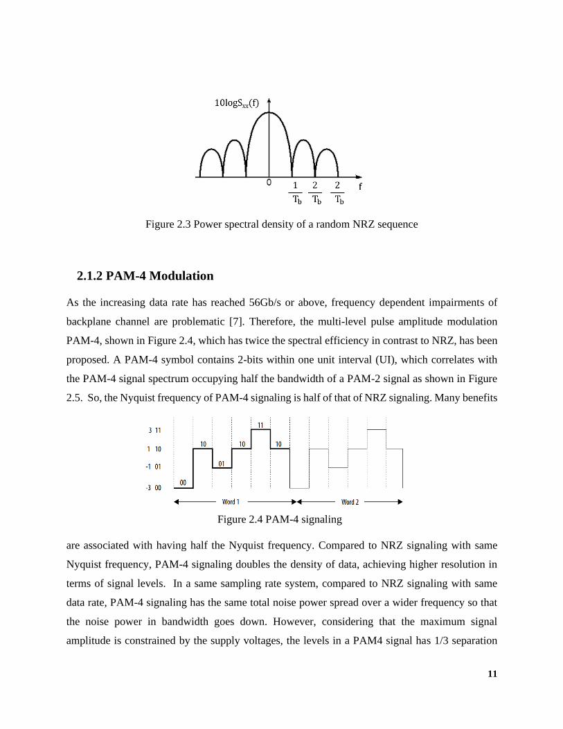
Figure 2.3 Power spectral density of a random NRZ sequence .................................................... 11
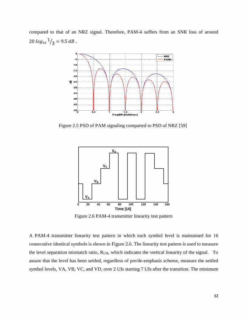
Figure 2.4 PAM-4 signaling ......................................................................................................... 11
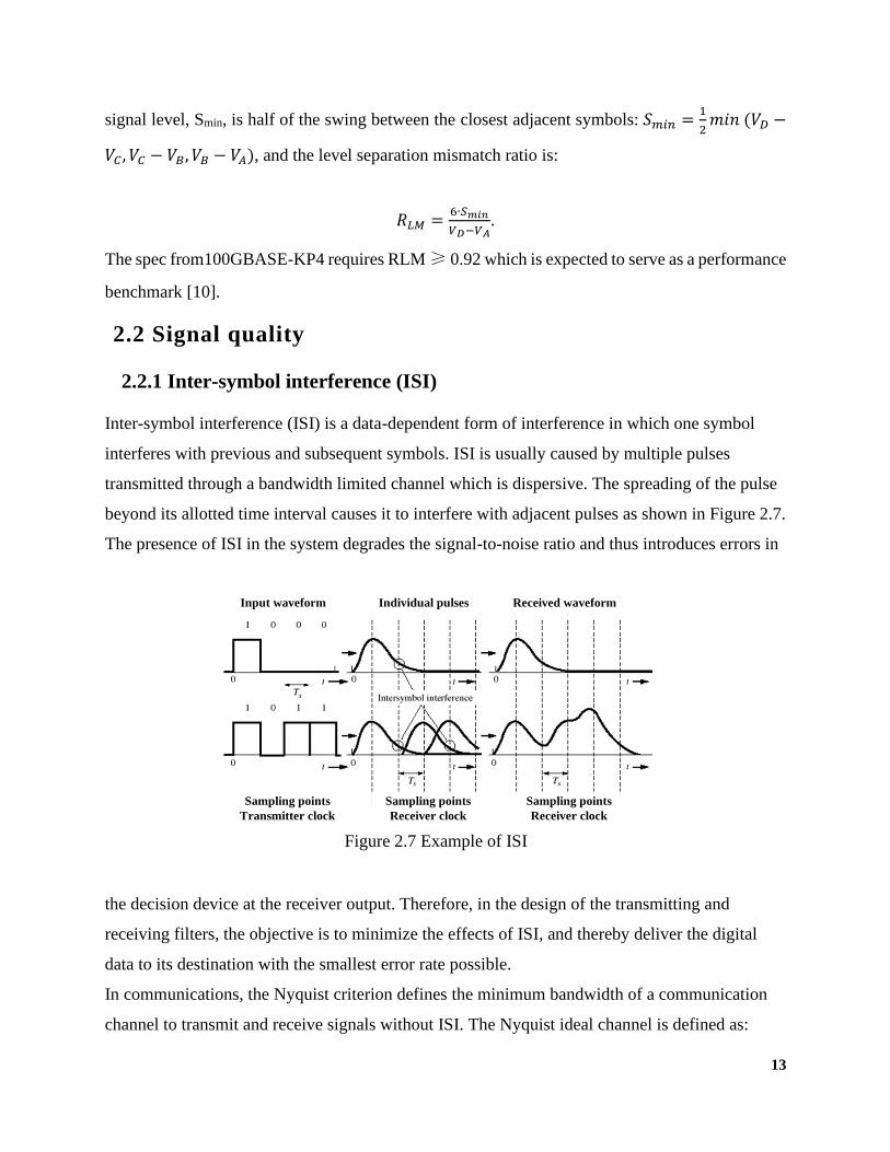
Figure 2.5 PSD of PAM signaling comparted to PSD of NRZ .................................................... 12
Figure 2.6 PAM-4 transmitter linearity test pattern ...................................................................... 12
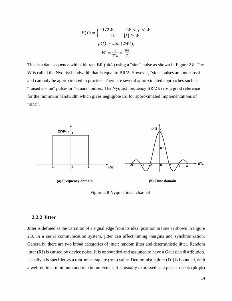
Figure 2.7 Example of ISI ............................................................................................................. 13
Figure 2.8 Nyquist ideal channel .................................................................................................. 14
Figure 2.9 Example of jitter .......................................................................................................... 15
Figure 2.10 Total jitter diagram tree ............................................................................................. 16
Figure 2.11 NRZ data eye diagram ............................................................................................... 16
Figure 2.12 Eye openings of an eye diagram ................................................................................ 17
Figure 2.13 BER contour in eye diagram ..................................................................................... 18
Figure 2.14 Bit error rate testing ................................................................................................... 19
Figure 2.15 Backplane channel ..................................................................................................... 20
Figure 2.16 Microstrip .................................................................................................................. 21
Figure 2.17 Stripline ..................................................................................................................... 21
Figure 2.18 Distributed element model of the transmission line .................................................. 22
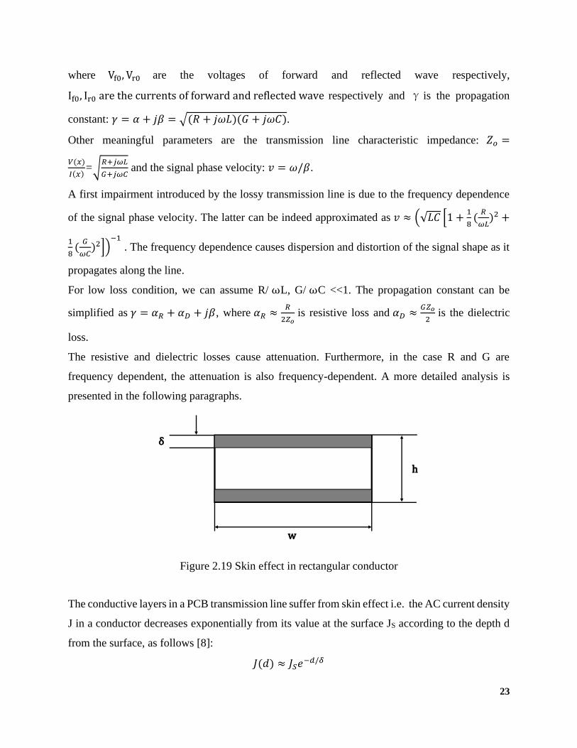
Figure 2.19 Skin effect in rectangular conductor.......................................................................... 23
Figure 2.20 Crossover between skin and dielectric loss ............................................................... 25
Figure 2.21 Simplified model of a backplane channel ................................................................. 26
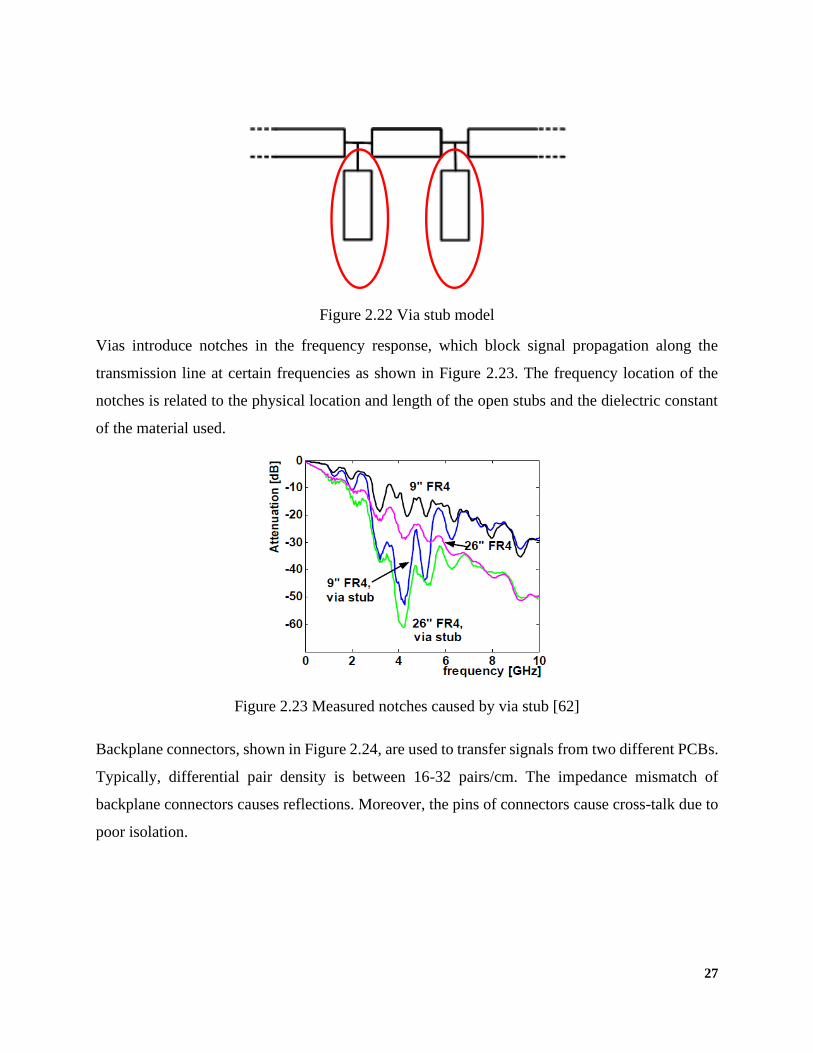
Figure 2.22 Via stub model ........................................................................................................... 27
Figure 2.23 Measured notches caused by via stub ........................................................................ 27
vi
Figure 2.24 Backplane connector ................................................................................................. 28
Figure 2.25 Flip-chip ball grid array package ............................................................................... 28
Figure 2.26 Measured frequency response of a FCBGA package ................................................ 29
Figure 2.27 Crosstalk .................................................................................................................... 29
Figure 2.28 ICR requirement ........................................................................................................ 30
Figure 3.1 Transceiver based on mixed signals equalization ....................................................... 33
Figure 3.2 Schematic of traditional CTLE and transfer function ................................................. 34
Figure 3.3 Frequency and symbol response of channel and CTLE .............................................. 35
Figure 3.4 Eye diagram of one-stage CTLE equalization ............................................................. 36
Figure 3.5 Frequency and symbol response of one-stage and cascaded CTLE comparison ........ 37
Figure 3.6 Eye diagram of a cascaded CTLE equalization ........................................................... 37
Figure 3.7 Schematic of a single CTLE with LF equalizer .......................................................... 38
Figure 3.8 Frequency and symbol response of the cascaded CTLE with/without LF equalizer .. 39
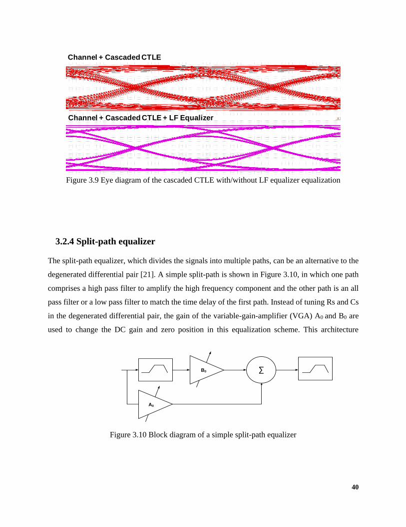
Figure 3.9 Eye diagram of the cascaded CTLE with/without LF equalizer equalization ............. 40
Figure 3.10 Block diagram of a simple split-path equalizer ......................................................... 40
Figure 3.11 Block diagram of an advanced split-path equalizer .................................................. 41
Figure 3.12 Schematic of the bandpass filter (a) and VGA (b) .................................................... 42
Figure 3.13 Shunt peaking schematic and equivalent small signal model ................................... 43
Figure 3.14 Frequency response of an amplifier with shunt peaking ........................................... 44
Figure 3.15 Schematic and simplified transfer function of shunt series peaking ......................... 44
Figure 3.16 Schematic of negative capacitance and simplified small signal model ..................... 45
Figure 3.17 Example of negative capacitance canceling .............................................................. 46
Figure 3.18 Equalizer adaptation concept ..................................................................................... 47
Figure 3.19 MSE adaptation concept ............................................................................................ 48
Figure 3.20 Cost function surface with uncorrelated state-signals ............................................... 48
Figure 4.1 Block diagram of the transversal CTLE and schematic of the block H(s) (single-ended
signals are used in the block diagram for better readability) ............................................. 50
Figure 4.2 MSE surface at 25Gb/s of the equalizer cascaded with a 20dB loss backplane channel
............................................................................................................................................ 51
Figure 4.3 MSE surface from a cascaded CTLE .......................................................................... 53
Figure 4.4 Simulated H(s) with different peaking inductors combinations .................................. 53
vii
Figure 4.5 Schematic of a tap amplifier ........................................................................................ 54
Figure 4.6 Tap amplifier topologies.............................................................................................. 56
Figure 4.7 Simulated trans-characteristics .................................................................................... 56
Figure 4.8 Chip photograph .......................................................................................................... 57
Figure 4.9 Measured transfer function of one stage H(s) of the transversal path ......................... 58
Figure 4.10 Experimental setup and loss of the different backplanes used for measurements. ... 58
Figure 4.11 Flow-chart of MMSE adaptation algorithm. ............................................................. 59
Figure 4.12 Eye diagrams after channel (20dB loss) and equalizer at data rate from 5Gb/s to
25Gb/s. ............................................................................................................................... 60
Figure 5.1 Application space of 56Gb/s links .............................................................................. 63
Figure 5.2 Receivers block diagram ............................................................................................. 65
Figure 5.3 VGA realized with resistive source degeneration (a) and frequency response (b) ..... 67
Figure 5.4 VGA based on cross-coupled differential pairs (a) and frequency response (b) ......... 67
Figure 5.5 Circuit topology of the realized VGA (a), gain vs frequency (b), gain vs input
amplitude (c) ...................................................................................................................... 68
Figure 5.6 Gain calibration of VGA ............................................................................................. 69
Figure 5.7 Circuit schematic of the continuous-time linear equalizer (a) and tuning of feedback
equalizer (b)........................................................................................................................ 70
Figure 5.8 Frequency response and eye diagrams at different steps of the CTLE adaptation. Mid-
frequency stage (a,b), low-frequency stage (c,d) and high-frequency stage (e,f) ............. 72
Figure 5.9 Temperature sensitivity of the CTLE transfer function. ............................................. 73
Figure 5.10 Chip photographs and breakdown of TX/RX power dissipation. ............................. 74
Figure 5.11 Experimental setup for the link tests (a) and TX-to-RX pulse response (b) ............. 74
Figure 5.12 BER contour (a) and bathtub (b) at 32Gb/s NRZ. BER contour (c) and bathtub (d) at
64Gb/s PAM-4 ................................................................................................................... 75
Figure 5.13 Jitter tolerance test at 64Gb/s PAM-4 @ BER=10-6 ................................................. 75
Figure 6.1 Architecture of the compete ADC based receiver ....................................................... 79
Figure 6.2112Gb/s PAM-4 analog front-end architecture ............................................................ 80
Figure 6.3 Circuit design flow-chart in 7nm FinFet technology .................................................. 81
Figure 6.4 Current density test circuit (a) and gain at Nyquist frequency versus current density(b)
............................................................................................................................................ 82
viii
Figure 6.5 Schematic of proposed CTLE (first parts)................................................................... 83
Figure 6.6 T-Coil peaking bandwidth extension ........................................................................... 84
Figure 6.7 Negative capacitance peaking enhancement ............................................................... 85
Figure 6.8 Transfer function of the of the first stage of the CTLE ............................................... 85
Figure 6.9 Transfer function the second stage of the CTLE ......................................................... 86
Figure 6.10 Large signal simulation of the complete analog-front-end ........................................ 86
Figure 6.11 Simulated AC response (a) and eye diagram (b) ....................................................... 87
ix
List of Tables
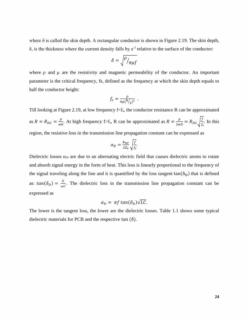
Table 2.1 Dielectric material ......................................................................................................... 25
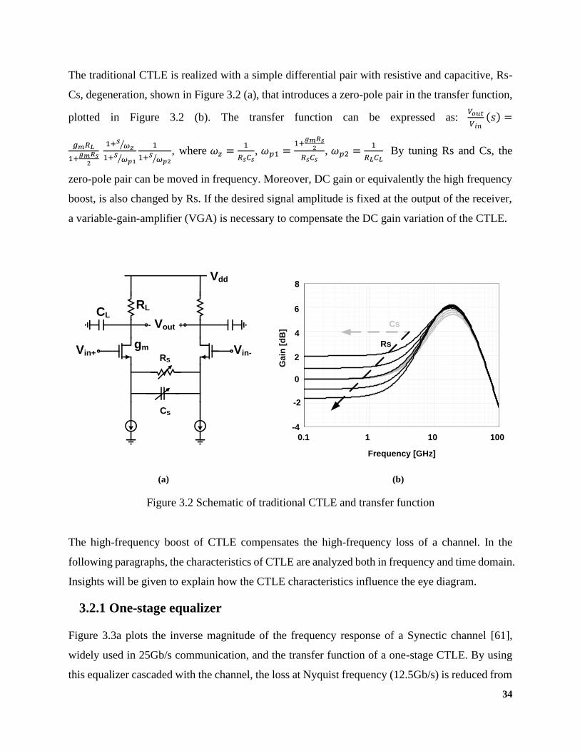
Table 3.1 Cursors in symbol response of the channel and one-stage CTLE ................................ 35
Table 3.2 Cursors in symbol response of the channel, one-stage and cascaded CTLE ................ 37
Table 3.3 Cursors in symbol response of the channel, cascaded CTLE and cascaded CTLE with
LF equalizer........................................................................................................................ 39
Table 4.1 Performance summary and comparison ........................................................................ 61
Table 5.1 Receiver summary and comparison. ............................................................................. 76

x
List of Acronyms
IoT Internet of Things
CAGR Compound Annual Growth Rate
EB Exabyte
BER Bit Error Rate
PCB Printed Circuit Board
FEC Forward Error Correction
DSP Digital Signal Processing
NRZ Non-Return-to-Zero
PAM-4 Paulse-Amplitue-Modulation-4
TX Transmitter
RX Receiver
ADC Analog-to-Digital Converter
CTLE Continuous-Time-Linear-Equalizer
FIR Finite Impulse Response
FFE Feedforward-Equalizer
DFE Decision-Feedback-Equalizer
AFE Analog Front-End
VGA Variable-Gain-Amplifier
PLL Phase-Locked Loop
CDR Clock-and-Data Recovery
UI Unit Interval
PSD Power Spectral Density
ISI Inter-Symbol Interference
BR Bit Rate
RJ Random Jitter
DJ Deterministic Jitter
DDJ Data Dependent Jitter

xi
BUJ Bounded Uncorrelated Jitter
FCBGA Flip-Chip Ball Grid Array
FEXT Far-End Crosstalk
NEXT Near-End Crosstalk
IL Insertion Loss
ICR Insertion Loss to Crosstalk Ratio
FOM Figure of Merit
LF Low Frequency
PVT Process-Voltage-Temperature
LMS Least-Mean-Squares
MSE Mean-Square-Errors
MMSE Minimum-Mean-Square-Errors
FVF Flipped-Voltage-Follower
CDF Common-Drain-Follower
TI Time-Interleaved

1
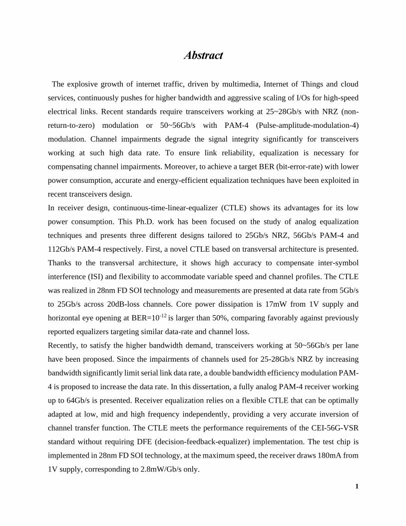
Abstract
The explosive growth of internet traffic, driven by multimedia, Internet of Things and cloud
services, continuously pushes for higher bandwidth and aggressive scaling of I/Os for high-speed
electrical links. Recent standards require transceivers working at 25~28Gb/s with NRZ (non-
return-to-zero) modulation or 50~56Gb/s with PAM-4 (Pulse-amplitude-modulation-4)
modulation. Channel impairments degrade the signal integrity significantly for transceivers
working at such high data rate. To ensure link reliability, equalization is necessary for
compensating channel impairments. Moreover, to achieve a target BER (bit-error-rate) with lower
power consumption, accurate and energy-efficient equalization techniques have been exploited in
recent transceivers design.
In receiver design, continuous-time-linear-equalizer (CTLE) shows its advantages for its low
power consumption. This Ph.D. work has been focused on the study of analog equalization
techniques and presents three different designs tailored to 25Gb/s NRZ, 56Gb/s PAM-4 and
112Gb/s PAM-4 respectively. First, a novel CTLE based on transversal architecture is presented.
Thanks to the transversal architecture, it shows high accuracy to compensate inter-symbol
interference (ISI) and flexibility to accommodate variable speed and channel profiles. The CTLE
was realized in 28nm FD SOI technology and measurements are presented at data rate from 5Gb/s
to 25Gb/s across 20dB-loss channels. Core power dissipation is 17mW from 1V supply and
horizontal eye opening at BER=10-12 is larger than 50%, comparing favorably against previously
reported equalizers targeting similar data-rate and channel loss.
Recently, to satisfy the higher bandwidth demand, transceivers working at 50~56Gb/s per lane
have been proposed. Since the impairments of channels used for 25-28Gb/s NRZ by increasing
bandwidth significantly limit serial link data rate, a double bandwidth efficiency modulation PAM-
4 is proposed to increase the data rate. In this dissertation, a fully analog PAM-4 receiver working
up to 64Gb/s is presented. Receiver equalization relies on a flexible CTLE that can be optimally
adapted at low, mid and high frequency independently, providing a very accurate inversion of
channel transfer function. The CTLE meets the performance requirements of the CEI-56G-VSR
standard without requiring DFE (decision-feedback-equalizer) implementation. The test chip is
implemented in 28nm FD SOI technology, at the maximum speed, the receiver draws 180mA from
1V supply, corresponding to 2.8mW/Gb/s only.
2
Electrical interfaces used with 100Gb/s singling are being investigated to satisfy the continual
growth of bandwidth demand. In the newer Ethernet standard, IEEE 802.3ck, one-single lane
100Gb/s interfaces are specified. In this thesis, a 112Gb/s PAM-4 analog front-end designed in
7nm FinFet technology is presented. The target is to be merged with an analog-to-digital converter
(ADC) based receiver so as to take advantage of high-performance digital signal processing (DSP)
in 7nm FinFet technology. However, significant changes in transistor behavior, scaled supply
voltage, and very different layout rules result in challenges in analog circuits design. Design
considerations regarding linearity and bandwidth of analog circuits in 7nm FinFet technology are
presented in this thesis. Simulation results prove the analog front-end can successfully recover
112Gb/s PAM-4 sequences transmitted through a 15dB Synectic channel.
3
Chapter 1 Introduction
1.1 Backgrounds
Internet services are extremely important in modern life. Nowadays, internet services like social
media, HD video streaming, cloud services, big data, and Internet of Things (IoT) have pushed
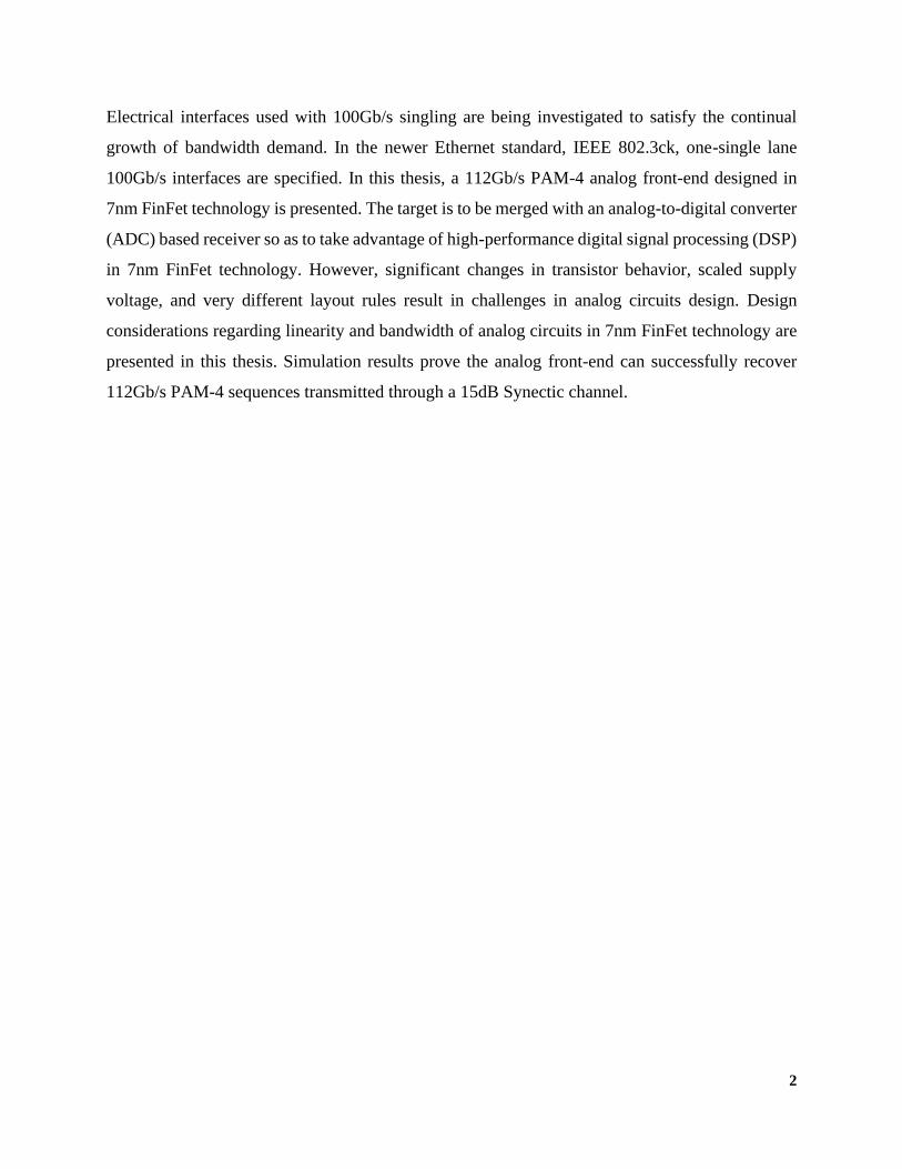
network traffic to grow exponentially. Most of the Internet services are being run in datacenters.
The data from Cisco white paper shows that by the year 2019, 99% of the global network traffic
is related to data centers [1]. Data centers could be treated as a “super-computer” in which there
are high-density interconnections of servers, often stacked in racks that are placed in row as shown
in Figure 1.1.
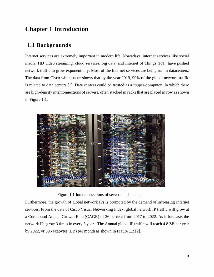
Furthermore, the growth of global network IPs is promoted by the demand of increasing Internet
services. From the data of Cisco Visual Networking Index, global network IP traffic will grow at
a Compound Annual Growth Rate (CAGR) of 26 percent from 2017 to 2022. As it forecasts the
network IPs grow 3 times in every 5 years. The Annual global IP traffic will reach 4.8 ZB per year
by 2022, or 396 exabytes (EB) per month as shown in Figure 1.2 [2].
Figure 1.1 Interconnections of servers in data center
4
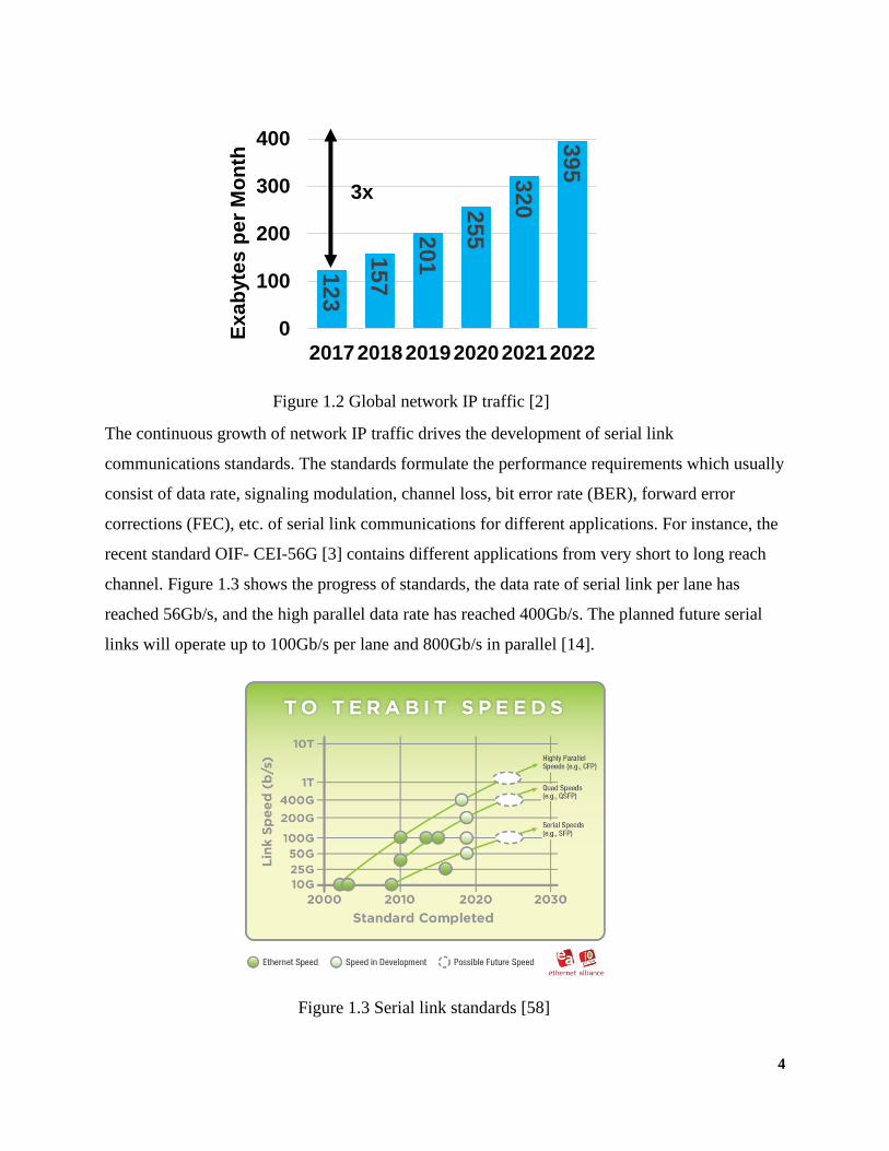
The continuous growth of network IP traffic drives the development of serial link
communications standards. The standards formulate the performance requirements which usually
consist of data rate, signaling modulation, channel loss, bit error rate (BER), forward error
corrections (FEC), etc. of serial link communications for different applications. For instance, the
recent standard OIF- CEI-56G [3] contains different applications from very short to long reach
channel. Figure 1.3 shows the progress of standards, the data rate of serial link per lane has
reached 56Gb/s, and the high parallel data rate has reached 400Gb/s. The planned future serial
links will operate up to 100Gb/s per lane and 800Gb/s in parallel [14].
Figure 1.2 Global network IP traffic [2]
12
3
15
7
201
25
5
320
39
50
100
200
300
400
201720182019202020212022
Ex
ab
yte
s p
er
Mo
nth
3x
Figure 1.3 Serial link standards [58]
5
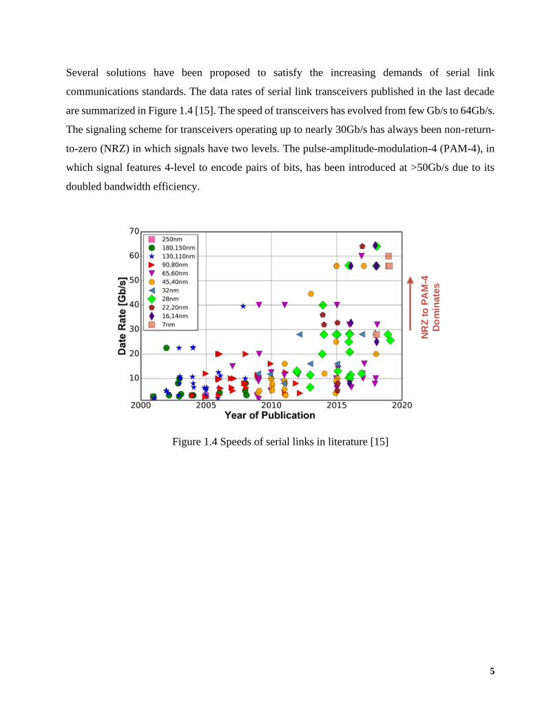
Several solutions have been proposed to satisfy the increasing demands of serial link
communications standards. The data rates of serial link transceivers published in the last decade
are summarized in Figure 1.4 [15]. The speed of transceivers has evolved from few Gb/s to 64Gb/s.
The signaling scheme for transceivers operating up to nearly 30Gb/s has always been non-return-
to-zero (NRZ) in which signals have two levels. The pulse-amplitude-modulation-4 (PAM-4), in
which signal features 4-level to encode pairs of bits, has been introduced at >50Gb/s due to its
doubled bandwidth efficiency.
Figure 1.4 Speeds of serial links in literature [15]
NR
Z t
o P
AM
-4
Do
min
ate
s
6
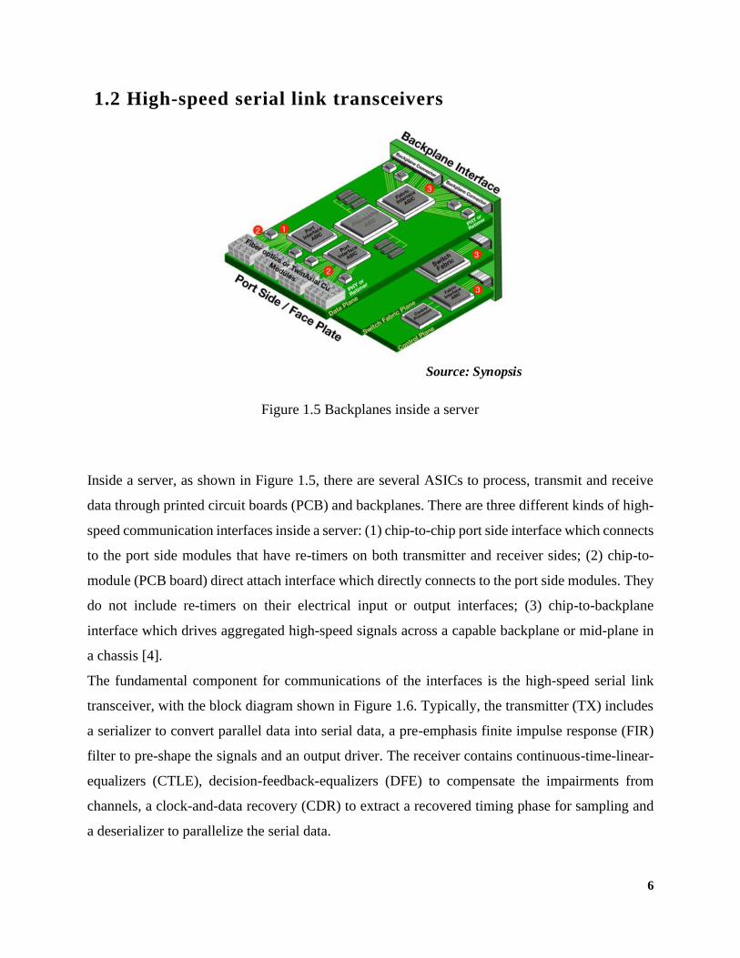
1.2 High-speed serial link transceivers
Inside a server, as shown in Figure 1.5, there are several ASICs to process, transmit and receive
data through printed circuit boards (PCB) and backplanes. There are three different kinds of high-
speed communication interfaces inside a server: (1) chip-to-chip port side interface which connects
to the port side modules that have re-timers on both transmitter and receiver sides; (2) chip-to-
module (PCB board) direct attach interface which directly connects to the port side modules. They
do not include re-timers on their electrical input or output interfaces; (3) chip-to-backplane
interface which drives aggregated high-speed signals across a capable backplane or mid-plane in
a chassis [4].
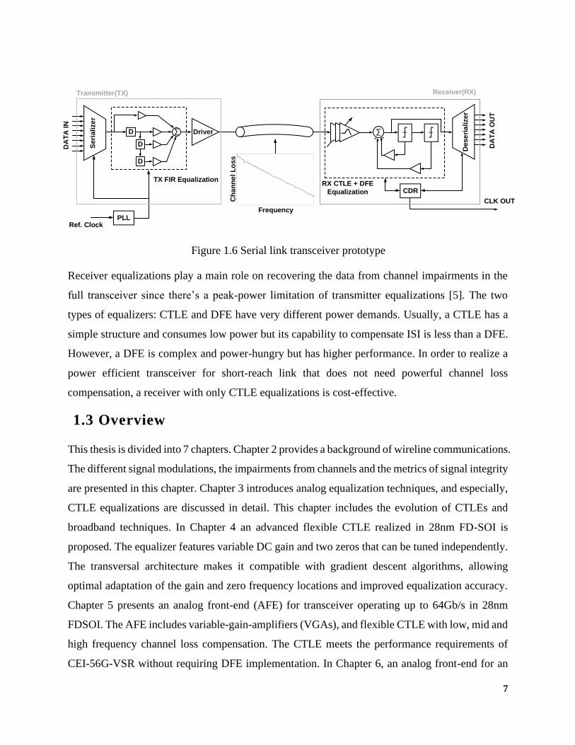
The fundamental component for communications of the interfaces is the high-speed serial link
transceiver, with the block diagram shown in Figure 1.6. Typically, the transmitter (TX) includes
a serializer to convert parallel data into serial data, a pre-emphasis finite impulse response (FIR)
filter to pre-shape the signals and an output driver. The receiver contains continuous-time-linear-
equalizers (CTLE), decision-feedback-equalizers (DFE) to compensate the impairments from
channels, a clock-and-data recovery (CDR) to extract a recovered timing phase for sampling and
a deserializer to parallelize the serial data.
Figure 1.5 Backplanes inside a server
Source: Synopsis
7
Receiver equalizations play a main role on recovering the data from channel impairments in the
full transceiver since there’s a peak-power limitation of transmitter equalizations [5]. The two
types of equalizers: CTLE and DFE have very different power demands. Usually, a CTLE has a
simple structure and consumes low power but its capability to compensate ISI is less than a DFE.
However, a DFE is complex and power-hungry but has higher performance. In order to realize a
power efficient transceiver for short-reach link that does not need powerful channel loss
compensation, a receiver with only CTLE equalizations is cost-effective.
1.3 Overview
This thesis is divided into 7 chapters. Chapter 2 provides a background of wireline communications.
The different signal modulations, the impairments from channels and the metrics of signal integrity
are presented in this chapter. Chapter 3 introduces analog equalization techniques, and especially,
CTLE equalizations are discussed in detail. This chapter includes the evolution of CTLEs and
broadband techniques. In Chapter 4 an advanced flexible CTLE realized in 28nm FD-SOI is
proposed. The equalizer features variable DC gain and two zeros that can be tuned independently.
The transversal architecture makes it compatible with gradient descent algorithms, allowing
optimal adaptation of the gain and zero frequency locations and improved equalization accuracy.
Chapter 5 presents an analog front-end (AFE) for transceiver operating up to 64Gb/s in 28nm
FDSOI. The AFE includes variable-gain-amplifiers (VGAs), and flexible CTLE with low, mid and
high frequency channel loss compensation. The CTLE meets the performance requirements of
CEI-56G-VSR without requiring DFE implementation. In Chapter 6, an analog front-end for an
Figure 1.6 Serial link transceiver prototype
PLL
Transmitter(TX)
Ref. Clock
DA
TA
IN
Frequency
Ch
an
ne
l L
oss
-20
-18
-16
-14
-12
-10
-8
-6
1E+07 4E+09 8E+09 1E+10 2E+10
Tit
le
Title
TX FIR Equalization
D
D
D
Driver
Seri
alize
r
CDRRX CTLE + DFE
Equalization
CLK OUT
--
Dese
ria
lizer
DA
TA
OU
T
Receiver(RX)

8
ADC-based receiver operating up to 112Gb/s in 7nm FinFet is presented. The analog front-end
comprises a variable-gain-amplifier (VGA), and a flexible CTLE with low, mid and high
frequency channel-loss compensation, followed by and a buffer. Particular care was paid to reach
adequate analog front-end linearity. Multiple broadband techniques are exploited in CTLE to
extend the operating frequency above 28GHz.
Finally, the Thesis is concluded with a summary and future work directions in Chapter 7.
9
Chapter 2 Background of wireline communications
2.1 Wireline communication signaling
2.1.1 NRZ Modulation
Pulse amplitude modulation is commonly employed in wireline communication signaling. NRZ
(non-return-to-zero) signaling with two-level pulse amplitude modulation as shown in Figure 2.1
has been widely used in high-speed serial link transmissions. In wireline communications, a NRZ
sequence is a binary sequence in which usually ones are represented by a positive voltage level
and zeros are represented by a negative voltage level.
As shown in Figure 2.2, a NRZ sequence x(t) can be expressed as: 𝑥(𝑡) = ∑ 𝑏𝑘𝑝(𝑡 − 𝑘𝑇𝑏𝑘 ),
where 𝑏𝑘 = ±𝑉0/2 and p(t) is the rectangular pulse function. As such, the signal x(t) is the sum
of the product of time-shifted replicas of the square pulse (p(t)) and bits (bk).
Vo: Amplitude
Tb: Bit Duration, also called Unit Interval (UI)
1/ Tb: Bit Rate
Figure 2.1 NRZ signals
Figure 2.2 NRZ sequence 𝑥(𝑡)
time
+p(t)
-p(t)
10
𝑥(𝑡) = 𝑝(𝑡) ∗ ∑ 𝑏𝑘 ∙ 𝛿(𝑡 − 𝑘𝑇𝑏𝑘 ) (* is convolution)
Defining:
𝑦(𝑡) =∑𝑏𝑘 ∙ 𝛿(𝑡 − 𝑘𝑇𝑏𝑘
)
the power spectral density (PSD) of x(t) can be expressed as:
𝑆𝑥𝑥(𝑓) = |𝑃(𝑓)|2𝑆𝑦𝑦(𝑓).
where P(f) is the Fourier transform of p(t):
𝑃(𝑓) = 𝑇𝑏 [𝑠𝑖𝑛(𝜋𝑓𝑇𝑏)
𝜋𝑓𝑇𝑏] .
If we assume the ‘ONES’ and ‘ZEROES’ have equal probability, the PSD of y(t) is:
𝑆𝑦𝑦(𝑓) = 𝑏𝑘
2
𝑇𝑏
and the PSD of x(t) results:
𝑆𝑥𝑥(𝑓) =𝑉𝑜
2
4𝑇𝑏|𝑃(𝑓)|2,
𝑆𝑥𝑥(𝑓) =𝑉𝑜
2
4𝑇𝑏 [
𝑠𝑖𝑛(𝜋𝑓𝑇𝑏)
𝜋𝑓𝑇𝑏]2
.
Figure 2.3 shows the PSD of x(t). It shows periodic behavior having power concentrated on a min
lobe and replicas at higher frequency. It is interesting to note that power is zero for the frequencies
𝑓 = 𝑛/𝑇𝑏 , where n is an integer number.
11
2.1.2 PAM-4 Modulation
As the increasing data rate has reached 56Gb/s or above, frequency dependent impairments of
backplane channel are problematic [7]. Therefore, the multi-level pulse amplitude modulation
PAM-4, shown in Figure 2.4, which has twice the spectral efficiency in contrast to NRZ, has been
proposed. A PAM-4 symbol contains 2-bits within one unit interval (UI), which correlates with
the PAM-4 signal spectrum occupying half the bandwidth of a PAM-2 signal as shown in Figure
2.5. So, the Nyquist frequency of PAM-4 signaling is half of that of NRZ signaling. Many benefits
are associated with having half the Nyquist frequency. Compared to NRZ signaling with same
Nyquist frequency, PAM-4 signaling doubles the density of data, achieving higher resolution in
terms of signal levels. In a same sampling rate system, compared to NRZ signaling with same
data rate, PAM-4 signaling has the same total noise power spread over a wider frequency so that
the noise power in bandwidth goes down. However, considering that the maximum signal
amplitude is constrained by the supply voltages, the levels in a PAM4 signal has 1/3 separation
Figure 2.3 Power spectral density of a random NRZ sequence
Figure 2.4 PAM-4 signaling
12
compared to that of an NRZ signal. Therefore, PAM-4 suffers from an SNR loss of around
20 𝑙𝑜𝑔1013⁄ = 9.5 𝑑𝐵 .
A PAM-4 transmitter linearity test pattern in which each symbol level is maintained for 16
consecutive identical symbols is shown in Figure 2.6. The linearity test pattern is used to measure
the level separation mismatch ratio, RLM, which indicates the vertical linearity of the signal. To
assure that the level has been settled, regardless of pre/de-emphasis scheme, measure the settled
symbol levels, VA, VB, VC, and VD, over 2 UIs starting 7 UIs after the transition. The minimum
Figure 2.5 PSD of PAM signaling comparted to PSD of NRZ [59]
Figure 2.6 PAM-4 transmitter linearity test pattern
VA
VB
VC
VD
0 20 40 60 80 100 120 140 160
Time [UI]
13
signal level, Smin, is half of the swing between the closest adjacent symbols: 𝑆𝑚𝑖𝑛 =1
2𝑚𝑖𝑛 (𝑉𝐷 −
𝑉𝐶 , 𝑉𝐶 − 𝑉𝐵, 𝑉𝐵 − 𝑉𝐴), and the level separation mismatch ratio is:
𝑅𝐿𝑀 =6∙𝑆𝑚𝑖𝑛
𝑉𝐷−𝑉𝐴.
The spec from100GBASE-KP4 requires RLM ≥ 0.92 which is expected to serve as a performance
benchmark [10].
2.2 Signal quality
2.2.1 Inter-symbol interference (ISI)
Inter-symbol interference (ISI) is a data-dependent form of interference in which one symbol
interferes with previous and subsequent symbols. ISI is usually caused by multiple pulses
transmitted through a bandwidth limited channel which is dispersive. The spreading of the pulse
beyond its allotted time interval causes it to interfere with adjacent pulses as shown in Figure 2.7.
The presence of ISI in the system degrades the signal-to-noise ratio and thus introduces errors in
the decision device at the receiver output. Therefore, in the design of the transmitting and
receiving filters, the objective is to minimize the effects of ISI, and thereby deliver the digital
data to its destination with the smallest error rate possible.
In communications, the Nyquist criterion defines the minimum bandwidth of a communication
channel to transmit and receive signals without ISI. The Nyquist ideal channel is defined as:
Figure 2.7 Example of ISI
Input waveform Individual pulses Received waveform
Sampling points
Receiver clock
Sampling points
Receiver clock
Sampling points
Transmitter clock
14
𝑃(𝑓) = {−1/2𝑊, −𝑊 < 𝑓 < 𝑊
0, |𝑓| ≥ 𝑊
𝑝(𝑡) = 𝑠𝑖𝑛𝑐(2𝑊𝑡),
𝑊 =1
2𝑇𝑏=
𝐵𝑅
2.
This is a data sequence with a bit rate BR (bit/s) using a "sinc" pulse as shown in Figure 2.8. The
W is called the Nyquist bandwidth that is equal to BR/2. However, "sinc" pulses are not causal
and can only be approximated in practice. There are several approximated approaches such as
“raised cosine” pulses or “square” pulses. The Nyquist frequency BR/2 keeps a good reference
for the minimum bandwidth which gives negligible ISI for approximated implementations of
“sinc”.
2.2.2 Jitter
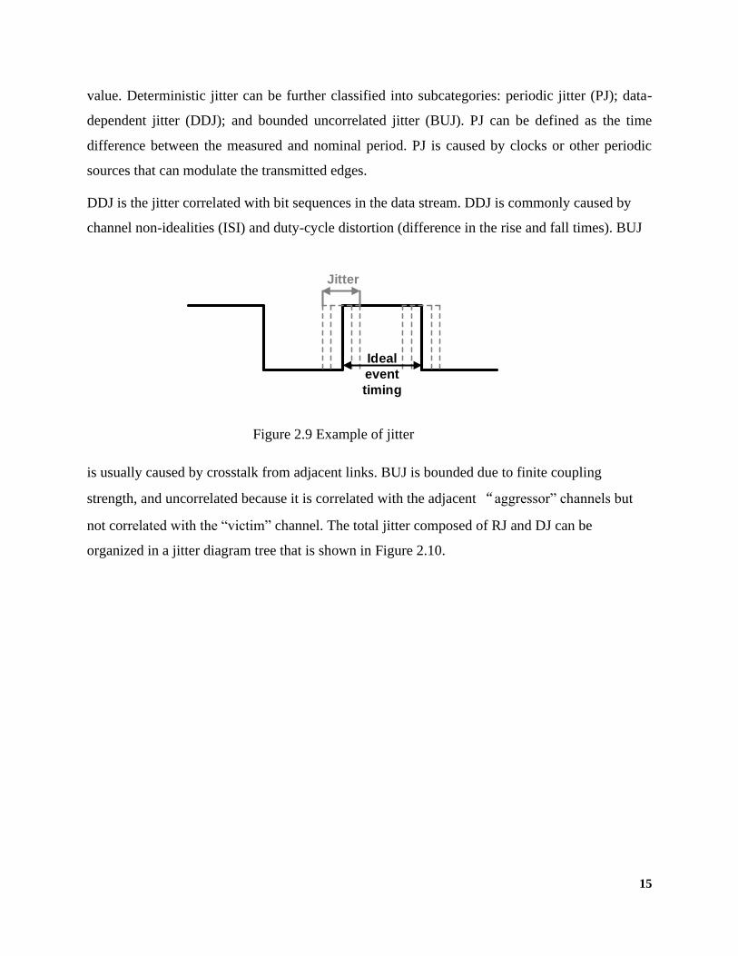
Jitter is defined as the variation of a signal edge from its ideal position in time as shown in Figure
2.9. In a serial communication system, jitter can affect timing margins and synchronization.
Generally, there are two broad categories of jitter: random jitter and deterministic jitter. Random
jitter (RJ) is caused by device noise. It is unbounded and assumed to have a Gaussian distribution.
Usually it is specified as a root-mean-square (rms) value. Deterministic jitter (DJ) is bounded, with
a well-defined minimum and maximum extent. It is usually expressed as a peak-to-peak (pk-pk)
(a) Frequency domain (b) Time domain
Figure 2.8 Nyquist ideal channel
2WP(f)1
0 1-1 f/Wt/Tb-3
0.5
1
-2 -1 0 1 2 3
p(t)
15
value. Deterministic jitter can be further classified into subcategories: periodic jitter (PJ); data-
dependent jitter (DDJ); and bounded uncorrelated jitter (BUJ). PJ can be defined as the time
difference between the measured and nominal period. PJ is caused by clocks or other periodic
sources that can modulate the transmitted edges.
DDJ is the jitter correlated with bit sequences in the data stream. DDJ is commonly caused by
channel non-idealities (ISI) and duty-cycle distortion (difference in the rise and fall times). BUJ
is usually caused by crosstalk from adjacent links. BUJ is bounded due to finite coupling
strength, and uncorrelated because it is correlated with the adjacent “aggressor” channels but
not correlated with the “victim” channel. The total jitter composed of RJ and DJ can be
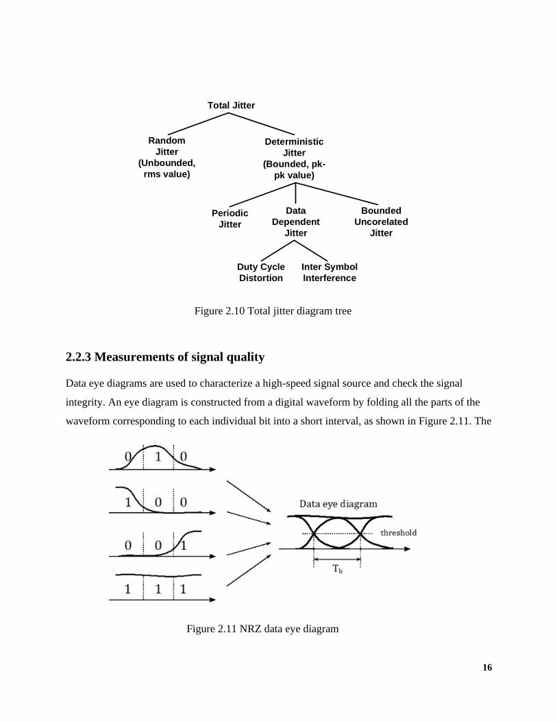
organized in a jitter diagram tree that is shown in Figure 2.10.
Figure 2.9 Example of jitter
Jitter
Ideal
event
timing
16
2.2.3 Measurements of signal quality
Data eye diagrams are used to characterize a high-speed signal source and check the signal
integrity. An eye diagram is constructed from a digital waveform by folding all the parts of the
waveform corresponding to each individual bit into a short interval, as shown in Figure 2.11. The
Figure 2.11 NRZ data eye diagram
Figure 2.10 Total jitter diagram tree
Total Jitter
Random
Jitter
(Unbounded,
rms value)
Deterministic
Jitter
(Bounded, pk-
pk value)
Periodic
Jitter
Data
Dependent
Jitter
Bounded
Uncorelated
Jitter
Duty Cycle
Distortion
Inter Symbol
Interference
17
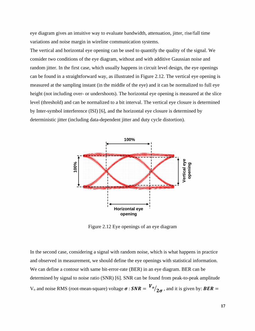
eye diagram gives an intuitive way to evaluate bandwidth, attenuation, jitter, rise/fall time
variations and noise margin in wireline communication systems.
The vertical and horizontal eye opening can be used to quantify the quality of the signal. We
consider two conditions of the eye diagram, without and with additive Gaussian noise and
random jitter. In the first case, which usually happens in circuit level design, the eye openings
can be found in a straightforward way, as illustrated in Figure 2.12. The vertical eye opening is
measured at the sampling instant (in the middle of the eye) and it can be normalized to full eye
height (not including over- or undershoots). The horizontal eye opening is measured at the slice
level (threshold) and can be normalized to a bit interval. The vertical eye closure is determined
by Inter-symbol interference (ISI) [6], and the horizontal eye closure is determined by
deterministic jitter (including data-dependent jitter and duty cycle distortion).
In the second case, considering a signal with random noise, which is what happens in practice
and observed in measurement, we should define the eye openings with statistical information.
We can define a contour with same bit-error-rate (BER) in an eye diagram. BER can be
determined by signal to noise ratio (SNR) [6]. SNR can be found from peak-to-peak amplitude
Vo and noise RMS (root-mean-square) voltage 𝝈 : 𝑺𝑵𝑹 = 𝑽𝒐
𝟐𝝈⁄ , and it is given by: 𝑩𝑬𝑹 =
Figure 2.12 Eye openings of an eye diagram
Horizontal eye
opening
Ve
rtic
al
ey
e
op
en
ing
100
%
100%
18
𝑸 (𝑽𝒐
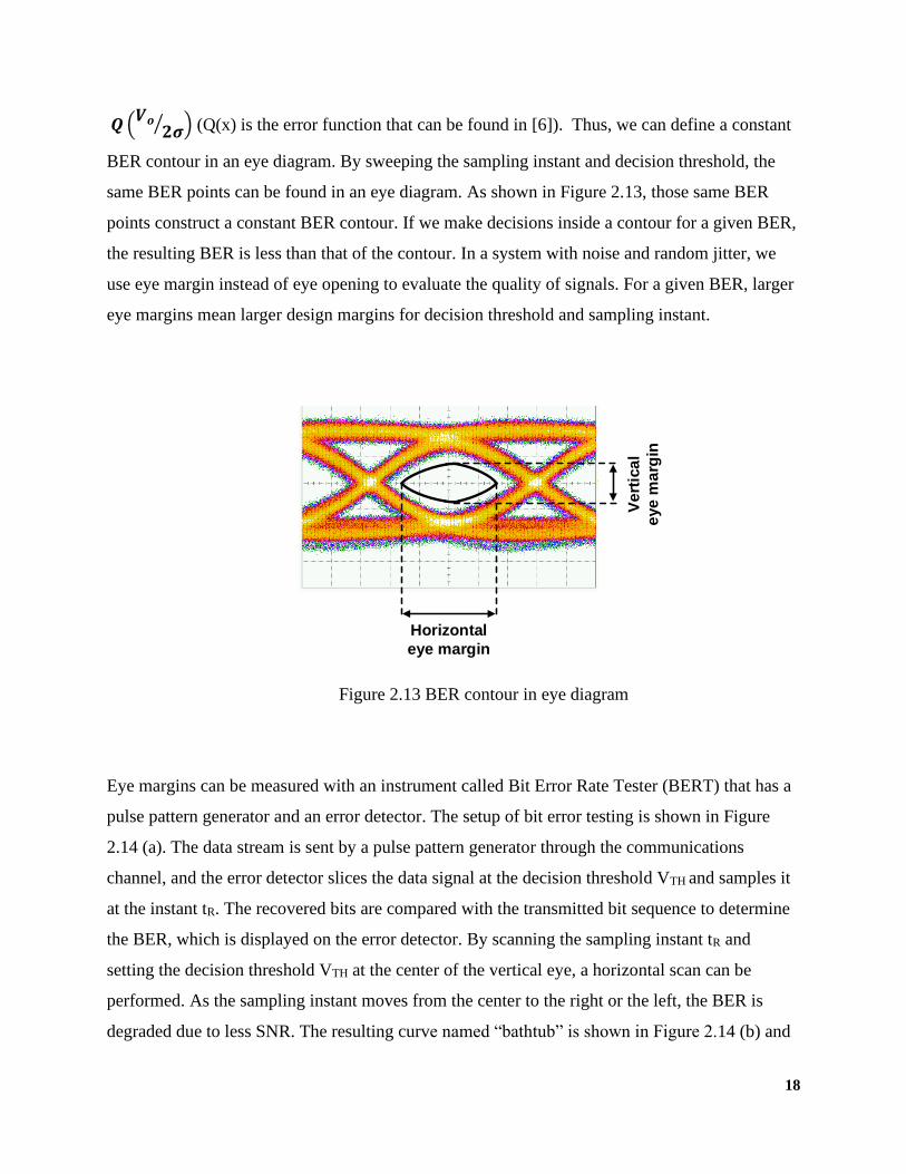
𝟐𝝈⁄ ) (Q(x) is the error function that can be found in [6]). Thus, we can define a constant
BER contour in an eye diagram. By sweeping the sampling instant and decision threshold, the
same BER points can be found in an eye diagram. As shown in Figure 2.13, those same BER
points construct a constant BER contour. If we make decisions inside a contour for a given BER,
the resulting BER is less than that of the contour. In a system with noise and random jitter, we
use eye margin instead of eye opening to evaluate the quality of signals. For a given BER, larger
eye margins mean larger design margins for decision threshold and sampling instant.
Eye margins can be measured with an instrument called Bit Error Rate Tester (BERT) that has a
pulse pattern generator and an error detector. The setup of bit error testing is shown in Figure
2.14 (a). The data stream is sent by a pulse pattern generator through the communications
channel, and the error detector slices the data signal at the decision threshold VTH and samples it
at the instant tR. The recovered bits are compared with the transmitted bit sequence to determine
the BER, which is displayed on the error detector. By scanning the sampling instant tR and
setting the decision threshold VTH at the center of the vertical eye, a horizontal scan can be
performed. As the sampling instant moves from the center to the right or the left, the BER is
degraded due to less SNR. The resulting curve named “bathtub” is shown in Figure 2.14 (b) and
Figure 2.13 BER contour in eye diagram
Ve
rtic
al
eye
ma
rgin
Horizontal
eye margin
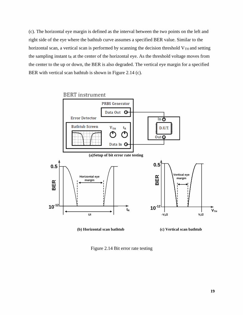
19
(c). The horizontal eye margin is defined as the interval between the two points on the left and
right side of the eye where the bathtub curve assumes a specified BER value. Similar to the
horizontal scan, a vertical scan is performed by scanning the decision threshold VTH and setting
the sampling instant tR at the center of the horizontal eye. As the threshold voltage moves from
the center to the up or down, the BER is also degraded. The vertical eye margin for a specified
BER with vertical scan bathtub is shown in Figure 2.14 (c).
(a)Setup of bit error rate testing
(b) Horizontal scan bathtub (c) Vertical scan bathtub
Figure 2.14 Bit error rate testing
BE
R
0.5
10-12
Horizontal eye
margin
UI
tR
BE
R
0.5
10-12
Vertical eye
margin
-V0/2 V0/2
VTH
20
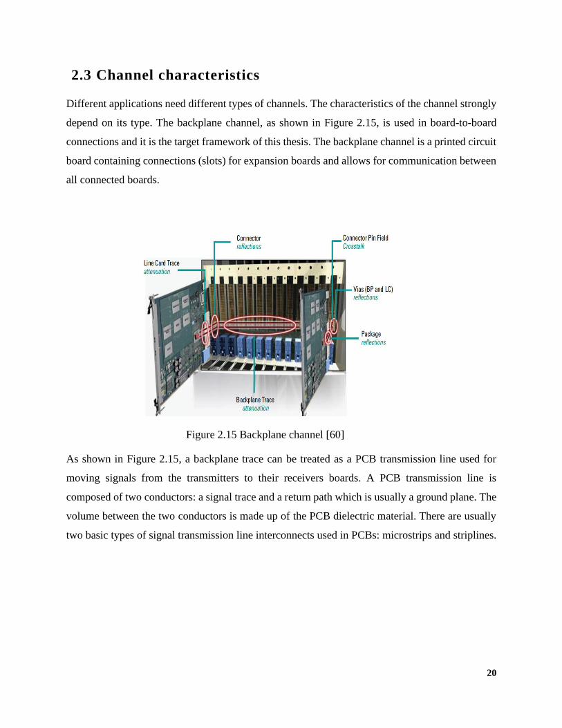
2.3 Channel characteristics
Different applications need different types of channels. The characteristics of the channel strongly
depend on its type. The backplane channel, as shown in Figure 2.15, is used in board-to-board
connections and it is the target framework of this thesis. The backplane channel is a printed circuit
board containing connections (slots) for expansion boards and allows for communication between
all connected boards.
As shown in Figure 2.15, a backplane trace can be treated as a PCB transmission line used for
moving signals from the transmitters to their receivers boards. A PCB transmission line is
composed of two conductors: a signal trace and a return path which is usually a ground plane. The
volume between the two conductors is made up of the PCB dielectric material. There are usually
two basic types of signal transmission line interconnects used in PCBs: microstrips and striplines.
Figure 2.15 Backplane channel [60]
21
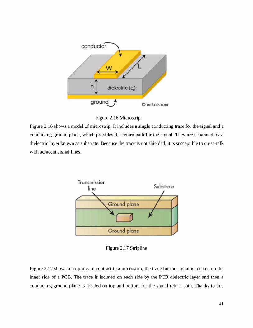
Figure 2.16 shows a model of microstrip. It includes a single conducting trace for the signal and a
conducting ground plane, which provides the return path for the signal. They are separated by a
dielectric layer known as substrate. Because the trace is not shielded, it is susceptible to cross-talk
with adjacent signal lines.
Figure 2.17 shows a stripline. In contrast to a microstrip, the trace for the signal is located on the
inner side of a PCB. The trace is isolated on each side by the PCB dielectric layer and then a
conducting ground plane is located on top and bottom for the signal return path. Thanks to this
Figure 2.16 Microstrip
Figure 2.17 Stripline
22
shielded structure, the stripline is much more robust to crosstalk and commonly employed in
backplanes.
There are several impairments in the backplane channel that degrade signal integrity at data rates
above a few gigabits per second. The frequency dependent impairments, reflections, and cross-
talk in backplane channels will be discussed in the following sections.
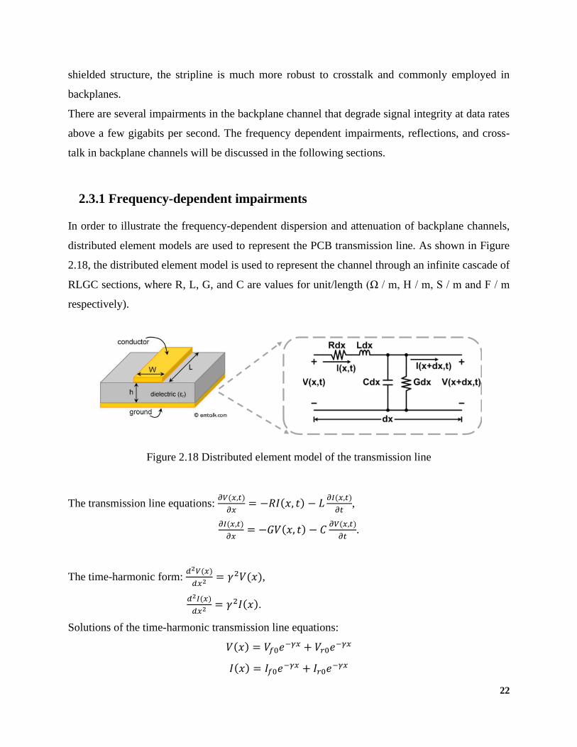
2.3.1 Frequency-dependent impairments
In order to illustrate the frequency-dependent dispersion and attenuation of backplane channels,
distributed element models are used to represent the PCB transmission line. As shown in Figure
2.18, the distributed element model is used to represent the channel through an infinite cascade of
RLGC sections, where R, L, G, and C are values for unit/length (Ω / m, H / m, S / m and F / m
respectively).
The transmission line equations: 𝜕𝑉(𝑥,𝑡)
𝜕𝑥= −𝑅𝐼(𝑥, 𝑡) − 𝐿
𝜕𝐼(𝑥,𝑡)
𝜕𝑡,
𝜕𝐼(𝑥,𝑡)
𝜕𝑥= −𝐺𝑉(𝑥, 𝑡) − 𝐶
𝜕𝑉(𝑥,𝑡)
𝜕𝑡.
The time-harmonic form: 𝑑2𝑉(𝑥)
𝑑𝑥2= 𝛾2𝑉(𝑥),
𝑑2𝐼(𝑥)
𝑑𝑥2= 𝛾2𝐼(𝑥).
Solutions of the time-harmonic transmission line equations:
𝑉(𝑥) = 𝑉𝑓0𝑒−𝛾𝑥 + 𝑉𝑟0𝑒
−𝛾𝑥
𝐼(𝑥) = 𝐼𝑓0𝑒−𝛾𝑥 + 𝐼𝑟0𝑒
−𝛾𝑥
Figure 2.18 Distributed element model of the transmission line
23
where Vf0, Vr0 are the voltages of forward and reflected wave respectively,
If0, Ir0 are the currents of forward and reflected wave respectively and γ is the propagation
constant: 𝛾 = 𝛼 + 𝑗𝛽 = √(𝑅 + 𝑗𝜔𝐿)(𝐺 + 𝑗𝜔𝐶).
Other meaningful parameters are the transmission line characteristic impedance: 𝑍𝑜 =
𝑉(𝑥)
𝐼(𝑥)=√
𝑅+𝑗𝜔𝐿
𝐺+𝑗𝜔𝐶 and the signal phase velocity: 𝑣 = 𝜔/𝛽.
A first impairment introduced by the lossy transmission line is due to the frequency dependence
of the signal phase velocity. The latter can be indeed approximated as 𝑣 ≈ (√𝐿𝐶 [1 +1
8(𝑅
𝜔𝐿)2 +
1
8(𝐺
𝜔𝐶)2])
−1
. The frequency dependence causes dispersion and distortion of the signal shape as it
propagates along the line.
For low loss condition, we can assume R/ ωL, G/ ωC <<1. The propagation constant can be
simplified as 𝛾 = 𝛼𝑅 + 𝛼𝐷 + 𝑗𝛽, where 𝛼𝑅 ≈𝑅
2𝑍𝑜 is resistive loss and 𝛼𝐷 ≈
𝐺𝑍𝑜
2 is the dielectric
loss.
The resistive and dielectric losses cause attenuation. Furthermore, in the case R and G are
frequency dependent, the attenuation is also frequency-dependent. A more detailed analysis is
presented in the following paragraphs.
The conductive layers in a PCB transmission line suffer from skin effect i.e. the AC current density
J in a conductor decreases exponentially from its value at the surface JS according to the depth d
from the surface, as follows [8]:
𝐽(𝑑) ≈ 𝐽𝑆𝑒−𝑑/𝛿
Figure 2.19 Skin effect in rectangular conductor
δ
w
h
24
where δ is called the skin depth. A rectangular conductor is shown in Figure 2.19. The skin depth,
δ, is the thickness where the current density falls by e-1 relative to the surface of the conductor:
𝛿 = √𝜌𝜋𝜇𝑓⁄
where and are the resistivity and magnetic permeability of the conductor. An important
parameter is the critical frequency, fs, defined as the frequency at which the skin depth equals to
half the conductor height:
𝑓𝑠 =𝜌
𝜋𝜇(ℎ 2⁄ )2 .
Till looking at Figure 2.19, at low frequency f<fs, the conductor resistance R can be approximated
as 𝑅 = 𝑅𝐷𝐶 =𝜌
𝑤ℎ. At high frequency f>fs, R can be approximated as 𝑅 =
𝜌
2𝑤𝛿= 𝑅𝐷𝐶√
𝑓
𝑓𝑠. In this
region, the resistive loss in the transmission line propagation constant can be expressed as
𝛼𝑅 =𝑅𝐷𝐶
2𝑍0√𝑓
𝑓𝑠.
Dielectric losses D are due to an alternating electric field that causes dielectric atoms to rotate
and absorb signal energy in the form of heat. This loss is linearly proportional to the frequency of
the signal traveling along the line and it is quantified by the loss tangent tan(δD) that is defined
as: 𝑡𝑎𝑛(𝛿𝐷) = 𝐺
𝜔𝐶. The dielectric loss in the transmission line propagation constant can be
expressed as
𝛼𝐷 = 𝜋𝑓 𝑡𝑎𝑛(𝛿𝐷)√𝐿𝐶.
The lower is the tangent loss, the lower are the dielectric losses. Table 1.1 shows some typical
dielectric materials for PCB and the respective tan (δ).
25
With the purpose of designing electronic equalizers for the PCB line imperfection it is useful to
introduce a closed-form expression for the total loss profile [61], combining resistive and dielectric
losses:
𝐿𝑜𝑠𝑠(𝑓) = 𝑒𝑥𝑝[−𝑘𝑠𝐿(1 + 𝑗)√𝑓 − 𝑘𝑑𝐿𝑓]
where L is the line length, ks and kd are coefficients related to the skin and dielectric loss
respectively. From the above equation, the impact of resistive loss, due to skin effect, rises with
the square root of the signal frequency while the dielectric loss rises linearly. Therefore, at low
frequency, the resistive loss is dominant, while as frequency increases, the dielectric loss becomes
Table 2.1 Dielectric material [8]
Figure 2.20 Crossover between skin and dielectric loss
26
relevant and the skin effect negligible. To gain insight, a typical channel transfer function is
depicted in Figure 2.20, where the loss is separated in the two contributions.
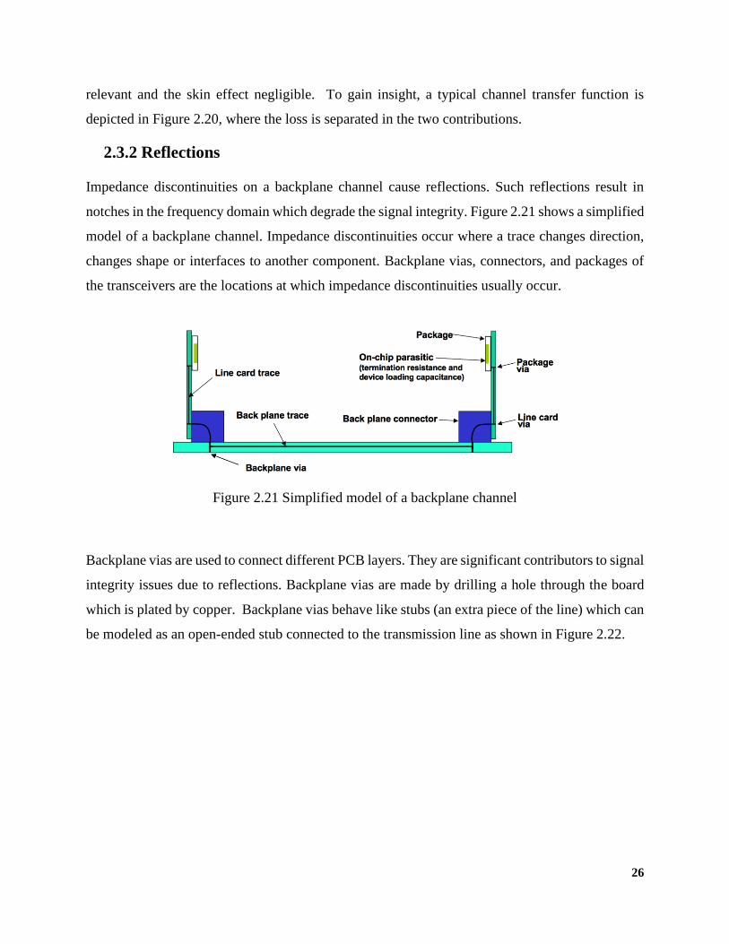
2.3.2 Reflections
Impedance discontinuities on a backplane channel cause reflections. Such reflections result in
notches in the frequency domain which degrade the signal integrity. Figure 2.21 shows a simplified
model of a backplane channel. Impedance discontinuities occur where a trace changes direction,
changes shape or interfaces to another component. Backplane vias, connectors, and packages of
the transceivers are the locations at which impedance discontinuities usually occur.
Backplane vias are used to connect different PCB layers. They are significant contributors to signal
integrity issues due to reflections. Backplane vias are made by drilling a hole through the board
which is plated by copper. Backplane vias behave like stubs (an extra piece of the line) which can
be modeled as an open-ended stub connected to the transmission line as shown in Figure 2.22.
Figure 2.21 Simplified model of a backplane channel
27
Vias introduce notches in the frequency response, which block signal propagation along the
transmission line at certain frequencies as shown in Figure 2.23. The frequency location of the
notches is related to the physical location and length of the open stubs and the dielectric constant
of the material used.
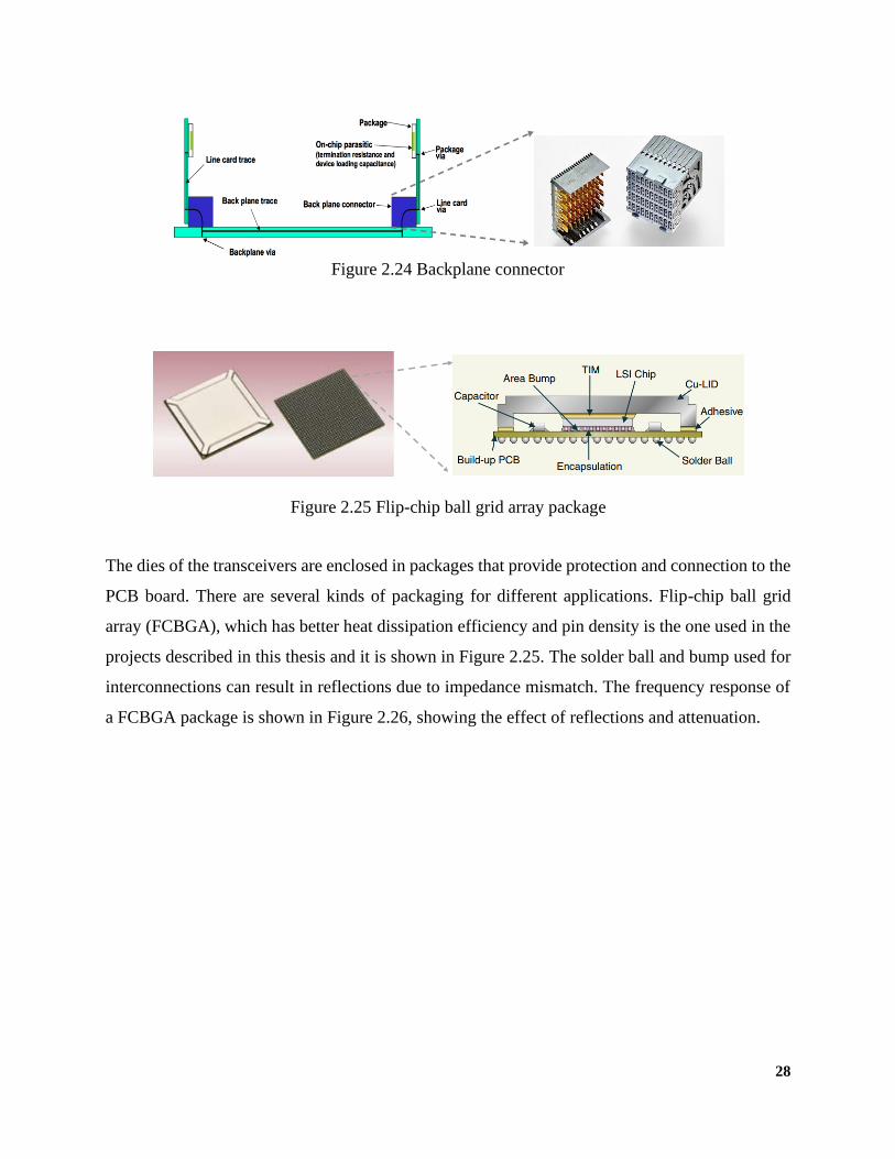
Backplane connectors, shown in Figure 2.24, are used to transfer signals from two different PCBs.
Typically, differential pair density is between 16-32 pairs/cm. The impedance mismatch of
backplane connectors causes reflections. Moreover, the pins of connectors cause cross-talk due to
poor isolation.
Figure 2.23 Measured notches caused by via stub [62]
Figure 2.22 Via stub model
28
The dies of the transceivers are enclosed in packages that provide protection and connection to the
PCB board. There are several kinds of packaging for different applications. Flip-chip ball grid
array (FCBGA), which has better heat dissipation efficiency and pin density is the one used in the
projects described in this thesis and it is shown in Figure 2.25. The solder ball and bump used for
interconnections can result in reflections due to impedance mismatch. The frequency response of
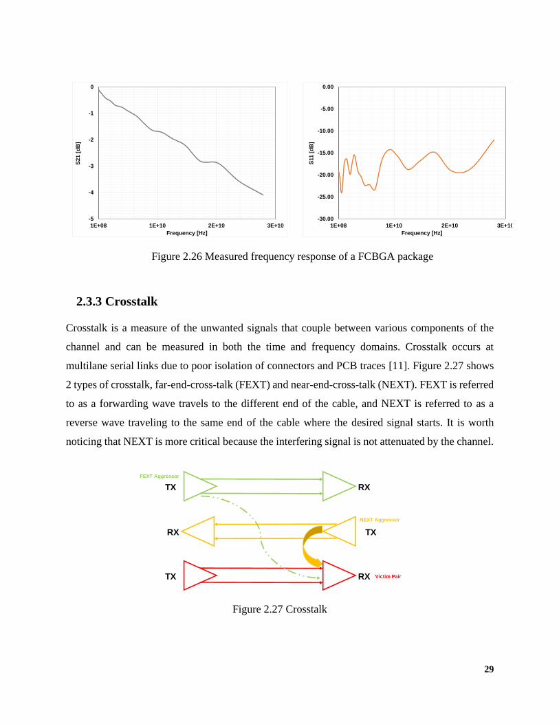
a FCBGA package is shown in Figure 2.26, showing the effect of reflections and attenuation.
Figure 2.25 Flip-chip ball grid array package
Figure 2.24 Backplane connector
29
2.3.3 Crosstalk
Crosstalk is a measure of the unwanted signals that couple between various components of the
channel and can be measured in both the time and frequency domains. Crosstalk occurs at
multilane serial links due to poor isolation of connectors and PCB traces [11]. Figure 2.27 shows
2 types of crosstalk, far-end-cross-talk (FEXT) and near-end-cross-talk (NEXT). FEXT is referred
to as a forwarding wave travels to the different end of the cable, and NEXT is referred to as a
reverse wave traveling to the same end of the cable where the desired signal starts. It is worth
noticing that NEXT is more critical because the interfering signal is not attenuated by the channel.
Figure 2.26 Measured frequency response of a FCBGA package
-5
-4
-3
-2
-1
0
1E+08 1E+10 2E+10 3E+10
S21
[d
B]
Frequency [Hz]
-30.00
-25.00
-20.00
-15.00
-10.00
-5.00
0.00
1E+08 1E+10 2E+10 3E+10
S11
[d
B]
Frequency [Hz]
Figure 2.27 Crosstalk
TX RX
TXRX
TX RX
FEXT Aggressor
NEXT Aggressor
Victim Pair
30
High-speed serial link transceivers use differential signaling to reject common mode aggressors.
However, crosstalk is canceled partially at high data rates because real differential pairs have
asymmetries that translate common-mode aggressors to differential mode.
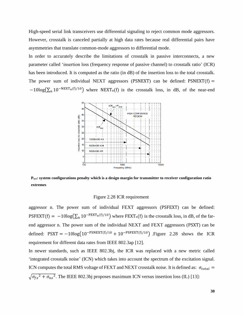
In order to accurately describe the limitations of crosstalk in passive interconnects, a new
parameter called ‘insertion loss (frequency response of passive channel) to crosstalk ratio’ (ICR)
has been introduced. It is computed as the ratio (in dB) of the insertion loss to the total crosstalk.
The power sum of individual NEXT aggressors (PSNEXT) can be defined: PSNEXT(f) =
−10log(∑ 10−NEXTn(f)/10n ) where NEXTn(f) is the crosstalk loss, in dB, of the near-end
aggressor n. The power sum of individual FEXT aggressors (PSFEXT) can be defined:
PSFEXT(f) = −10log(∑ 10−FEXTn(f)/10n ) where FEXTn(f) is the crosstalk loss, in dB, of the far-
end aggressor n. The power sum of the individual NEXT and FEXT aggressors (PSXT) can be
defined: PSXT = −10log(10−PSNEXT(f)/10 + 10−PSFEXT(f)/10) .Figure 2.28 shows the ICR
requirement for different data rates from IEEE 802.3ap [12].
In newer standards, such as IEEE 802.3bj, the ICR was replaced with a new metric called
‘integrated crosstalk noise’ (ICN) which takes into account the spectrum of the excitation signal.
ICN computes the total RMS voltage of FEXT and NEXT crosstalk noise. It is defined as: 𝜎𝑡𝑜𝑡𝑎𝑙 =
√𝜎𝑓𝑥2 + 𝜎𝑛𝑥2. The IEEE 802.3bj proposes maximum ICN versus insertion loss (IL) [13]:
Psys: system configurations penalty which is a design margin for transmitter to receiver configuration ratio
extremes
Figure 2.28 ICR requirement

31
𝜎𝑡𝑜𝑡𝑎𝑙 ≤ {8 4𝑑𝐵 ≤ 𝐼𝐿 ≤ 10.4𝑑𝐵
12.1 − 0.393 ∗ 𝐼𝐿(𝑑𝐵) 10.4𝑑𝐵 < 𝐼𝐿 ≤ 22.64𝑑𝐵.
32
Chapter 3 Analog equalization techniques
Abstract
A continuous-time-linear equalizer is a peaking filter with high-frequency gain boosting transfer
function that effectively compensates the frequency attenuation and dispersion of a channel. A
continuous-time equalizer requires less power consumption and smaller chip area compared to a
decision feedback equalizer (DFE), and thus it is an attractive solution for low-power high-speed
serial receivers. In this chapter, the evolution of CTLEs is introduced. In order to provide precise
equalizations, the CTLE evolves from one stage to multiple stages, and the low frequency equalizer
is introduced to remove the residual ISI due to skin effect. As an alternative to conventional CTLEs,
the split-path equalizer, which divides the signals into multiple paths is presented. Tanks to the
split-path structure, the CTLE can tune DC gain and zeros’ frequency independently. So that it
gives more flexibility to shape the transfer function. Broadband techniques are helpful to extend
the operating frequency of CTLEs. Inductive peaking and negative capacitance techniques that
are widely implemented in tens of Gb/s transceivers are introduced.
3.1 Introduction
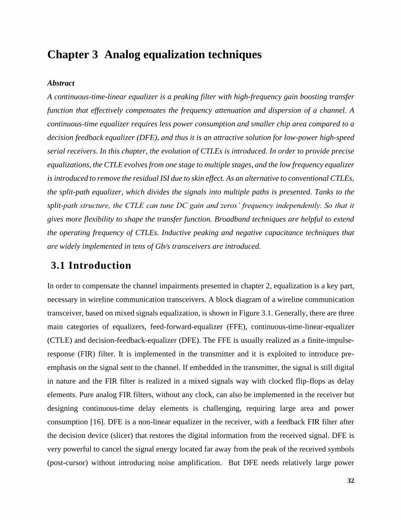
In order to compensate the channel impairments presented in chapter 2, equalization is a key part,
necessary in wireline communication transceivers. A block diagram of a wireline communication
transceiver, based on mixed signals equalization, is shown in Figure 3.1. Generally, there are three
main categories of equalizers, feed-forward-equalizer (FFE), continuous-time-linear-equalizer
(CTLE) and decision-feedback-equalizer (DFE). The FFE is usually realized as a finite-impulse-
response (FIR) filter. It is implemented in the transmitter and it is exploited to introduce pre-
emphasis on the signal sent to the channel. If embedded in the transmitter, the signal is still digital
in nature and the FIR filter is realized in a mixed signals way with clocked flip-flops as delay
elements. Pure analog FIR filters, without any clock, can also be implemented in the receiver but
designing continuous-time delay elements is challenging, requiring large area and power
consumption [16]. DFE is a non-linear equalizer in the receiver, with a feedback FIR filter after
the decision device (slicer) that restores the digital information from the received signal. DFE is
very powerful to cancel the signal energy located far away from the peak of the received symbols
(post-cursor) without introducing noise amplification. But DFE needs relatively large power
33
consumption and hardware complexity and therefore several receivers in short reach links are
implemented with only the CTLEs for power and area savings [17]. Traditionally, the CTLE is
realized with a differential pair degenerated by a parallel resistance-capacitance impedance that
introduces a zero-pole pair to boost the high frequency gain and compensate the high frequency
loss of the channel. However, state-of-the-art CTLE evolved from this simple implementation
toward more complicated structures, e.g. with a split-path approach [18]. The CTLE is always
present and plays a major role in shaping the transfer function of the receiver. A more in-depth
analysis of CTLE characteristics, both in frequency domain and time domain, is presented in this
chapter. Moreover, to satisfy the increasing data rate requirements, necessitating circuits operating
at higher and higher frequency, broadband circuit techniques implemented in state-of-the-art
CTLEs are also introduced in this chapter. Typically, a receiver with only CTLE is able to
compensate channel loss at Nyquist frequency up to 20dB [25] [28].
3.2 CTLE operation and evolution
State-of-the-art wireline communication transceivers must embrace and specify faster data rates to
satisfy the increasing bandwidth demand of the communication infrastructure. To achieve a good
Figure of Merit (FOM), transceivers employ CTLE as a low-cost, low power option. This drives a
continuous evolution of the CTLE to support higher speed and improve equalization performances.
Figure 3.1 Transceiver based on mixed signals equalization
PLL
TX RX
De
se
ria
lize
r
Se
ria
lize
r
CDR
Ref. Clock
Td Td
∑
Td
∑ ∑ ∑
TX FIR Equalization
∑--
RX CTLE + DFE EqualizationT
X D
AT
A
RX
DA
TA
Frequency
Ch
an
ne
l L
os
s
-20
-18
-16
-14
-12
-10
-8
-6
1E+07 4E+09 8E+09 1E+10 2E+10
Tit
le
Title
34
The traditional CTLE is realized with a simple differential pair with resistive and capacitive, Rs-
Cs, degeneration, shown in Figure 3.2 (a), that introduces a zero-pole pair in the transfer function,
plotted in Figure 3.2 (b). The transfer function can be expressed as: 𝑉𝑜𝑢𝑡
𝑉𝑖𝑛(𝑠) =
𝑔𝑚𝑅𝐿
1+𝑔𝑚𝑅𝑠
2
1+𝑠 𝜔𝑧⁄
1+𝑠 𝜔𝑝1⁄
1
1+𝑠 𝜔𝑝2⁄, where 𝜔𝑧 =
1
𝑅𝑠𝐶𝑠, 𝜔𝑝1 =
1+𝑔𝑚𝑅𝑠
2
𝑅𝑠𝐶𝑠, 𝜔𝑝2 =
1
𝑅𝐿𝐶𝐿 By tuning Rs and Cs, the
zero-pole pair can be moved in frequency. Moreover, DC gain or equivalently the high frequency
boost, is also changed by Rs. If the desired signal amplitude is fixed at the output of the receiver,
a variable-gain-amplifier (VGA) is necessary to compensate the DC gain variation of the CTLE.
The high-frequency boost of CTLE compensates the high-frequency loss of a channel. In the
following paragraphs, the characteristics of CTLE are analyzed both in frequency and time domain.
Insights will be given to explain how the CTLE characteristics influence the eye diagram.
3.2.1 One-stage equalizer
Figure 3.3a plots the inverse magnitude of the frequency response of a Synectic channel [61],
widely used in 25Gb/s communication, and the transfer function of a one-stage CTLE. By using
this equalizer cascaded with the channel, the loss at Nyquist frequency (12.5Gb/s) is reduced from
(a) (b)
Figure 3.2 Schematic of traditional CTLE and transfer function
Vin+ Vin-RS
gm
Vdd
CS
Vout- +
RLCL
-4
-2
0
2
4
6
8
1E+08 1E+09 1E+10 1E+11
Tit
le
Title
Frequency [GHz]
0.1
6
4
8G
ain
[d
B]
2
-2
1 10 100
0
-4
Cs
Rs
35
16.8dB to 12dB. Figure 3.3b shows the single-symbol response of the channel alone and of the
channel with the cascaded CTLE. Clearly, the addition of the CTLE reduces the pulse-spreading
effect across the bit boundary. Looking at the eye diagrams, shown in Figure 3.4., the inter-symbol
interference is reduced by introducing the CTLE after the channel.
Looking again at Figure 3.3, the inverse of the channel response has a sharper slope than the
response of the one-stage CTLE at Nyquist frequency. This is attributed to the dielectric loss of
the channel, relevant as the operation frequency increases.
(a) (b)
Figure 3.3 Frequency and symbol response of channel and CTLE
0
5
10
15
20
1.00E+08 1.00E+09 1.00E+10 1.00E+11
0.1
15
10
20
Gain
[d
B]
1 10 100
5
0
16.8 dB
4.8dB
Frequency [GHz]
Inverse channel
One-stage CTLE
-2.00E-01
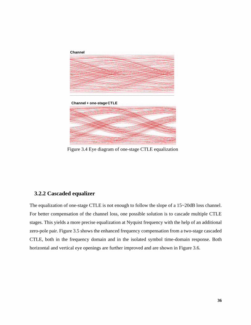
0.00E+00
2.00E-01
4.00E-01
6.00E-01
8.00E-01
1.00E+00
1.20E+00
0 1E-10 2E-10 3E-10 4E-10 5E-10
CTLE PUSLE NORM (V) CHANNEL PULSE NORM (V)
Time [ns]0
0.6
0.4
1.2
No
rmalize
d
Am
pli
tud
e
0.2
0
0.1 0.2 0.3
0.8
1
0.4
Channel
One-stage CTLE
0.5
Table 3.1 Cursors in symbol response of the channel and one-stage CTLE
1st pre-
cursor
1st post-
cursor
2nd post-
cursor
3rd post-
cursor
Channel 0.20 0.57 0.25 0.13
One-stage
CTLE0.13 0.40 0.14 0.08
36
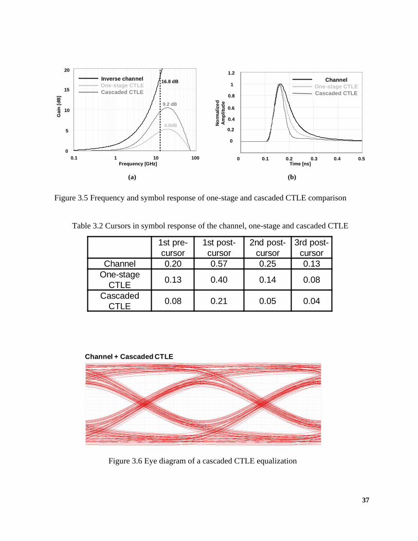
3.2.2 Cascaded equalizer
The equalization of one-stage CTLE is not enough to follow the slope of a 15~20dB loss channel.
For better compensation of the channel loss, one possible solution is to cascade multiple CTLE
stages. This yields a more precise equalization at Nyquist frequency with the help of an additional
zero-pole pair. Figure 3.5 shows the enhanced frequency compensation from a two-stage cascaded
CTLE, both in the frequency domain and in the isolated symbol time-domain response. Both
horizontal and vertical eye openings are further improved and are shown in Figure 3.6.
Figure 3.4 Eye diagram of one-stage CTLE equalization
Channel
Channel + one-stage CTLE
37
(a) (b)
Figure 3.5 Frequency and symbol response of one-stage and cascaded CTLE comparison
0.1
15
10
20
Gain
[d
B]
1 10 100
5
0
Frequency [GHz]
0
5
10
15
20
1.00E+08 1.00E+09 1.00E+10 1.00E+11
16.8 dB
4.8dB
9.2 dB
Inverse channel
One-stage CTLE
Cascaded CTLE
-2.00E-01
0.00E+00
2.00E-01
4.00E-01
6.00E-01
8.00E-01
1.00E+00
1.20E+00
0 1E-10 2E-10 3E-10 4E-10 5E-10
CTLE PUSLE NORM (V) CHANNEL PULSE NORM (V) CTLE 2 pulse (V)
Time [ns]0
0.6
0.4
1.2
No
rmalize
d
Am
pli
tud
e
0.2
0
0.8
1Channel
One-stage CTLE
Cascaded CTLE
0.1 0.2 0.3 0.4 0.5
Table 3.2 Cursors in symbol response of the channel, one-stage and cascaded CTLE
1st pre-
cursor
1st post-
cursor
2nd post-
cursor
3rd post-
cursor
Channel 0.20 0.57 0.25 0.13
One-stage
CTLE0.13 0.40 0.14 0.08
Cascaded
CTLE0.08 0.21 0.05 0.04
Figure 3.6 Eye diagram of a cascaded CTLE equalization
Channel + Cascaded CTLE
38
3.2.3 Low frequency equalizer
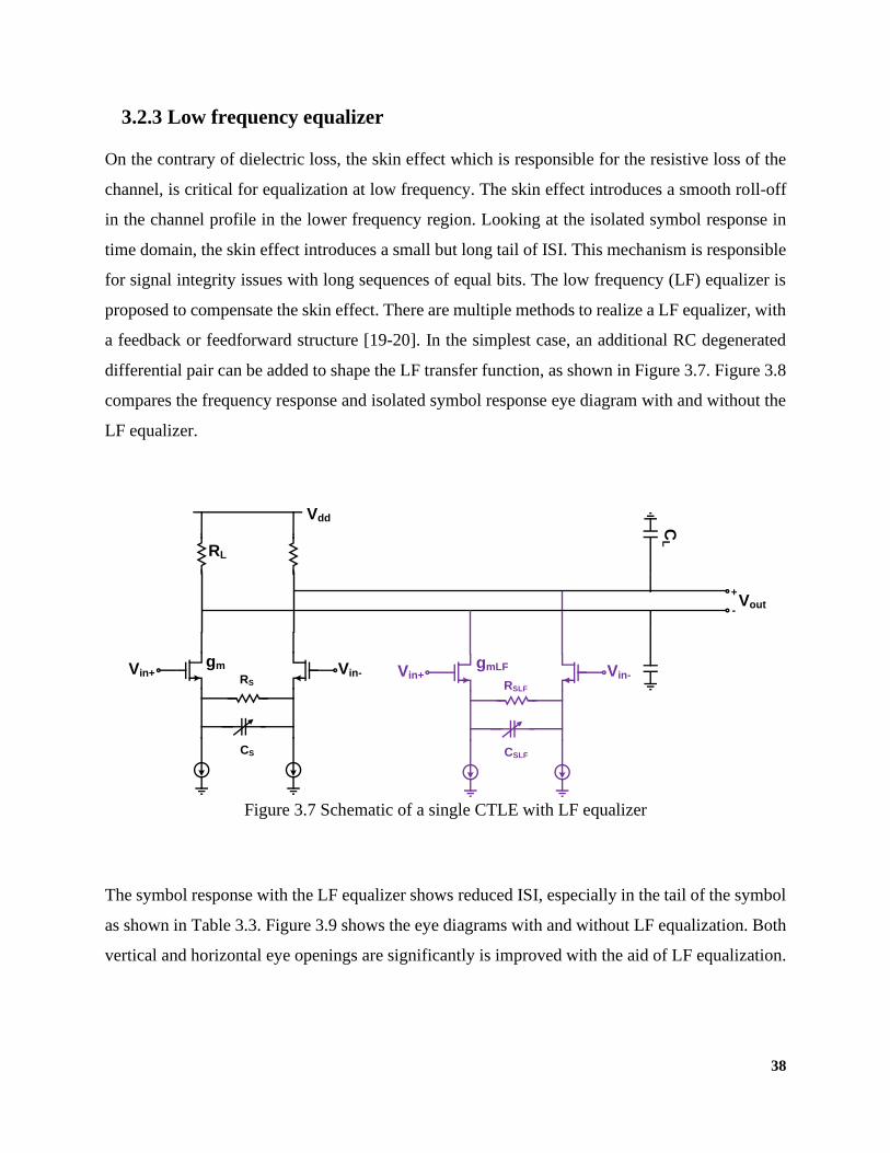
On the contrary of dielectric loss, the skin effect which is responsible for the resistive loss of the
channel, is critical for equalization at low frequency. The skin effect introduces a smooth roll-off
in the channel profile in the lower frequency region. Looking at the isolated symbol response in
time domain, the skin effect introduces a small but long tail of ISI. This mechanism is responsible
for signal integrity issues with long sequences of equal bits. The low frequency (LF) equalizer is
proposed to compensate the skin effect. There are multiple methods to realize a LF equalizer, with
a feedback or feedforward structure [19-20]. In the simplest case, an additional RC degenerated
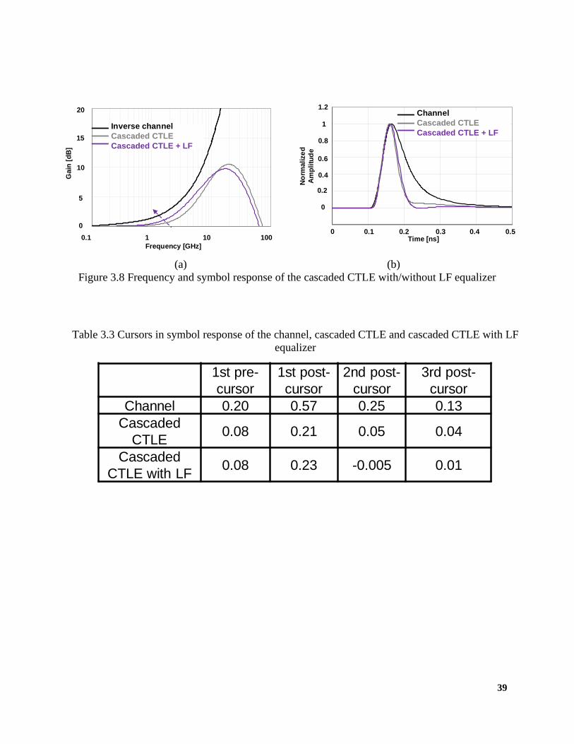
differential pair can be added to shape the LF transfer function, as shown in Figure 3.7. Figure 3.8
compares the frequency response and isolated symbol response eye diagram with and without the
LF equalizer.
The symbol response with the LF equalizer shows reduced ISI, especially in the tail of the symbol
as shown in Table 3.3. Figure 3.9 shows the eye diagrams with and without LF equalization. Both
vertical and horizontal eye openings are significantly is improved with the aid of LF equalization.
Figure 3.7 Schematic of a single CTLE with LF equalizer
Vin+ Vin-RS
gm
Vdd
CS
Vout-
+
RL
CL
Vin+ Vin-RSLF
gmLF
CSLF
39
(a) (b)
Figure 3.8 Frequency and symbol response of the cascaded CTLE with/without LF equalizer
0
5
10
15
20
1.00E+08 1.00E+09 1.00E+10 1.00E+11
0.1
15
10
20
Gain
[d
B]
1 10 100
5
0
Frequency [GHz]
Inverse channel
Cascaded CTLE
Cascaded CTLE + LF
-2.00E-01
0.00E+00
2.00E-01
4.00E-01
6.00E-01
8.00E-01
1.00E+00
1.20E+00
0 1E-10 2E-10 3E-10 4E-10 5E-10
CHANNEL PULSE NORM (V) CTLE 2 pulse (V) CTLE 2 pulse (V)
Time [ns]0
0.6
0.4
1.2
No
rmalize
d
Am
pli
tud
e
0.2
0
0.8
1
Channel
Cascaded CTLE
Cascaded CTLE + LF
0.1 0.2 0.3 0.4 0.5
Table 3.3 Cursors in symbol response of the channel, cascaded CTLE and cascaded CTLE with LF
equalizer
1st pre-
cursor
1st post-
cursor
2nd post-
cursor
3rd post-
cursor
Channel 0.20 0.57 0.25 0.13
Cascaded
CTLE0.08 0.21 0.05 0.04
Cascaded
CTLE with LF0.08 0.23 -0.005 0.01
40
3.2.4 Split-path equalizer
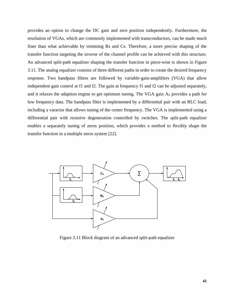
The split-path equalizer, which divides the signals into multiple paths, can be an alternative to the
degenerated differential pair [21]. A simple split-path is shown in Figure 3.10, in which one path
comprises a high pass filter to amplify the high frequency component and the other path is an all
pass filter or a low pass filter to match the time delay of the first path. Instead of tuning Rs and Cs
in the degenerated differential pair, the gain of the variable-gain-amplifier (VGA) A0 and B0 are
used to change the DC gain and zero position in this equalization scheme. This architecture
Figure 3.9 Eye diagram of the cascaded CTLE with/without LF equalizer equalization
Channel + Cascaded CTLE
Channel + Cascaded CTLE + LF Equalizer
Figure 3.10 Block diagram of a simple split-path equalizer
A0
B0
41
provides an option to change the DC gain and zero position independently. Furthermore, the
resolution of VGAs, which are commonly implemented with transconductors, can be made much
finer than what achievable by trimming Rs and Cs. Therefore, a more precise shaping of the
transfer function targeting the inverse of the channel profile can be achieved with this structure.
An advanced split-path equalizer shaping the transfer function in piece-wise is shown in Figure
3.11. The analog equalizer consists of three different paths in order to create the desired frequency
response. Two bandpass filters are followed by variable-gain-amplifiers (VGA) that allow
independent gain control at f1 and f2. The gain at frequency f1 and f2 can be adjusted separately,
and it relaxes the adaption engine to get optimum tuning. The VGA gain A0 provides a path for
low frequency data. The bandpass filter is implemented by a differential pair with an RLC load,
including a varactor that allows tuning of the center frequency. The VGA is implemented using a
differential pair with resistive degeneration controlled by switches. The split-path equalizer
enables a separately tuning of zeros position, which provides a method to flexibly shape the
transfer function in a multiple zeros system [22].
Figure 3.11 Block diagram of an advanced split-path equalizer
C0
B0
A0
f1
f2
f1 f2
42
3.3 Broadband techniques
As the operating frequency of analog equalizers increases, broadband techniques are necessary to
extend the bandwidth of the gain stages. There are several ways to extend bandwidth, in this
chapter the inductive peaking and negative cap canceling techniques will be presented.
3.3.1 Inductive peaking
With the advent of monolithic inductors, inductive peaking techniques have become feasible
in integrated circuits. The idea is to allow the capacitance that limits the bandwidth to resonate
with an inductor, thereby improving the speed. The resonance must, of course, occur with minimal
peaking and overshoot so as to provide a well-behaved response to random data.
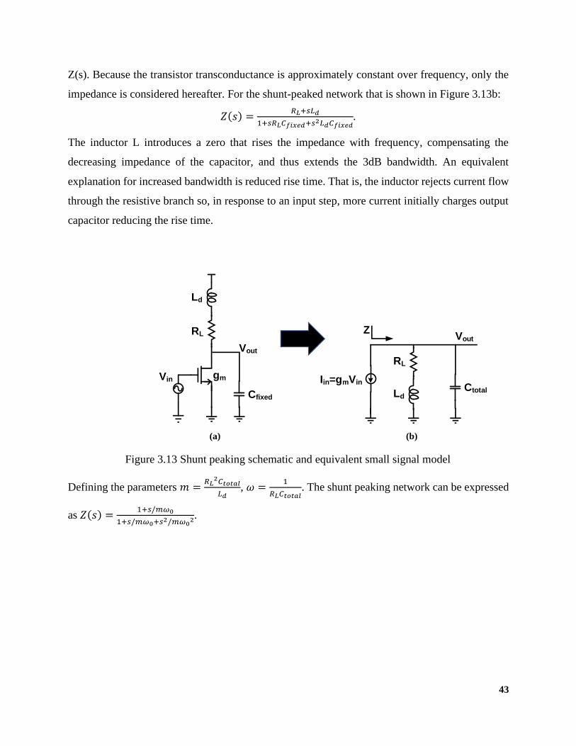
Shunt peaking
Shunt peaking is a bandwidth extension technique in which an inductor connected in series with
the load resistor shunts the output capacitor. The simplified schematic showing this technique is
reported in Figure 3.13. Treating the transistor as a small-signal dependent current source, the gain
is simply the product of the transistor transconductance, gm, and the impedance of the passive load,
(a) (b)
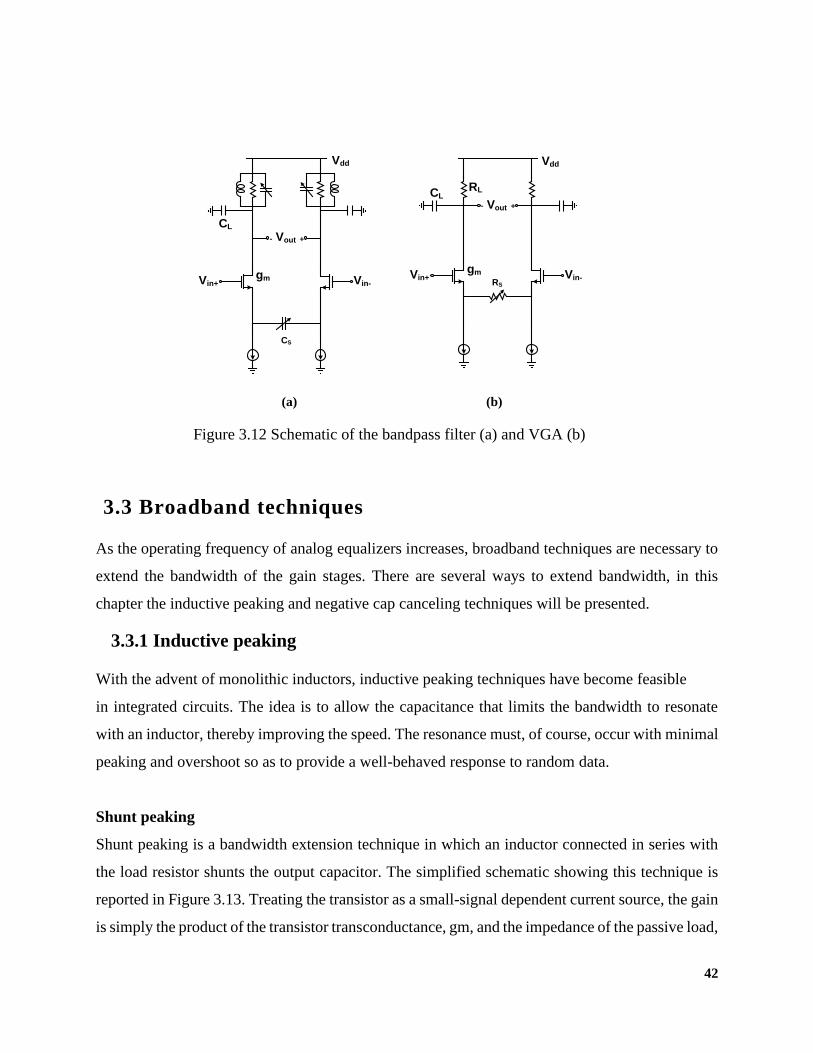
Figure 3.12 Schematic of the bandpass filter (a) and VGA (b)
Vin+ Vin-gm
Vdd
CS
Vout- +
CL
Vin+ Vin-RS
gm
Vdd
Vout- +
RLCL
43
Z(s). Because the transistor transconductance is approximately constant over frequency, only the
impedance is considered hereafter. For the shunt-peaked network that is shown in Figure 3.13b:
𝑍(𝑠) =𝑅𝐿+𝑠𝐿𝑑
1+𝑠𝑅𝐿𝐶𝑓𝑖𝑥𝑒𝑑+𝑠2𝐿𝑑𝐶𝑓𝑖𝑥𝑒𝑑
.
The inductor L introduces a zero that rises the impedance with frequency, compensating the
decreasing impedance of the capacitor, and thus extends the 3dB bandwidth. An equivalent
explanation for increased bandwidth is reduced rise time. That is, the inductor rejects current flow
through the resistive branch so, in response to an input step, more current initially charges output
capacitor reducing the rise time.
Defining the parameters 𝑚 =𝑅𝐿
2𝐶𝑡𝑜𝑡𝑎𝑙
𝐿𝑑, 𝜔 =
1
𝑅𝐿𝐶𝑡𝑜𝑡𝑎𝑙. The shunt peaking network can be expressed
as 𝑍(𝑠) =1+𝑠/𝑚𝜔0
1+𝑠/𝑚𝜔0+𝑠2/𝑚𝜔02.
(a) (b)
Figure 3.13 Shunt peaking schematic and equivalent small signal model
RL
Ld
Cfixed
Vin
Vout
gm
RL
LdCtotal
Iin=gmVin
ZVout
44
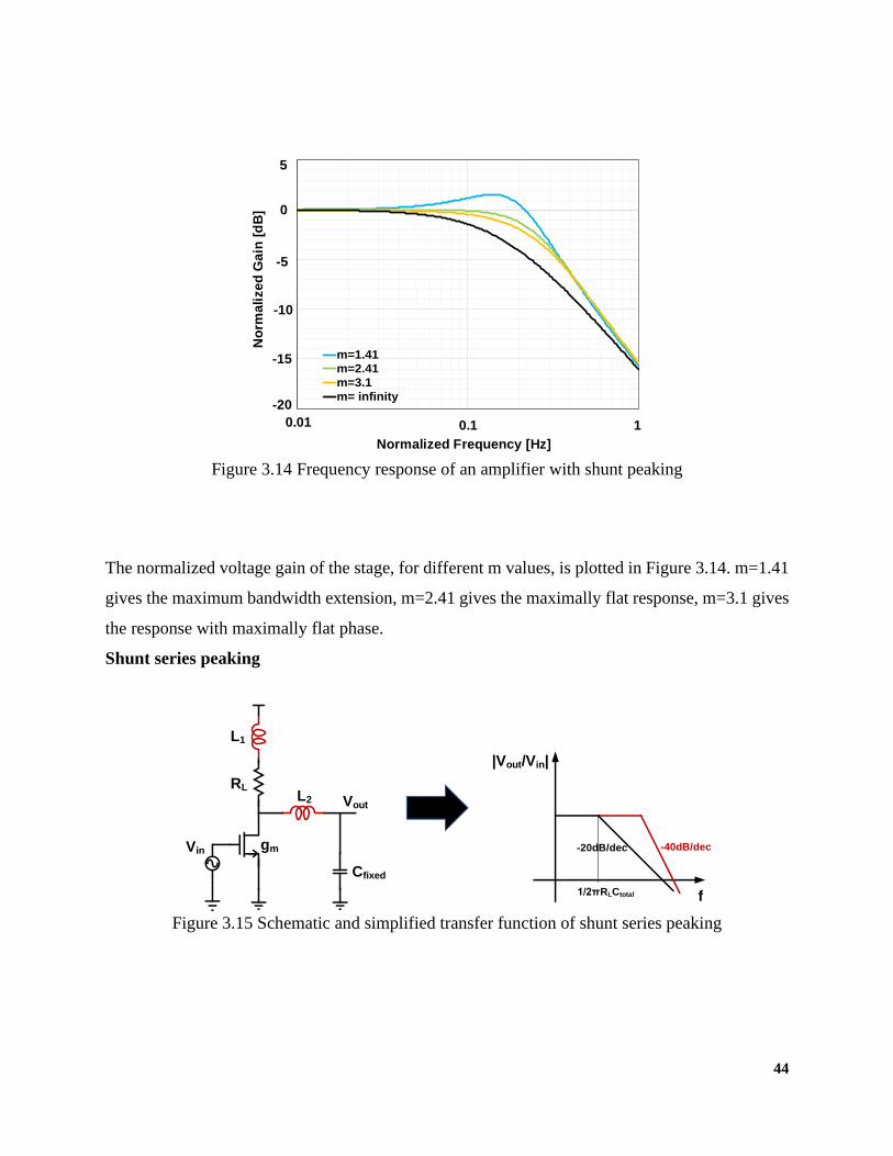
The normalized voltage gain of the stage, for different m values, is plotted in Figure 3.14. m=1.41
gives the maximum bandwidth extension, m=2.41 gives the maximally flat response, m=3.1 gives
the response with maximally flat phase.
Shunt series peaking
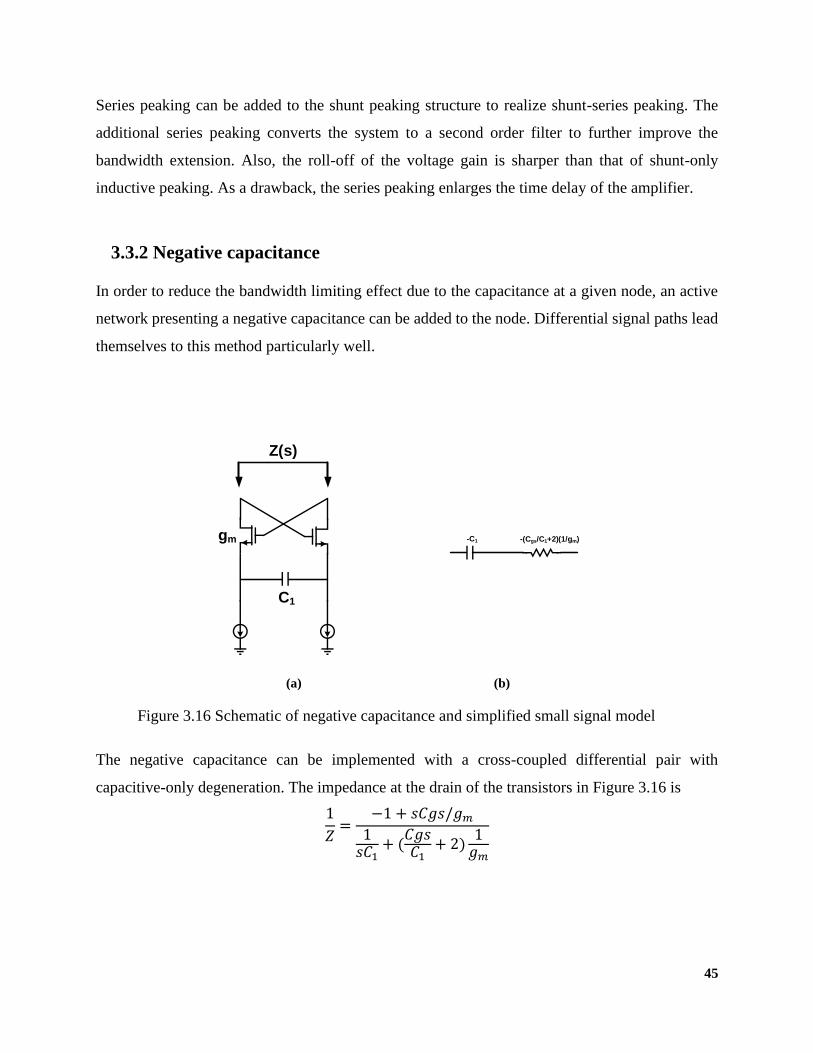
Figure 3.15 Schematic and simplified transfer function of shunt series peaking
RL
L1
Cfixed
Vin
Vout
gm
L2
f
|Vout/Vin|
-20dB/dec -40dB/dec
1/2πRLCtotal
Figure 3.14 Frequency response of an amplifier with shunt peaking
-20
-15
-10
-5
0
5
0.01 0.1 1
No
rma
lize
d G
ain
[d
B]
Normalized Frequency [Hz]
m=1.41
m=2.41
m=3.1
m= infinity
Normalized Frequency [Hz]
0.01 0.1
-15
-10
-5
0
5
No
rma
lize
d G
ain
[d
B]
1
-20
45
Series peaking can be added to the shunt peaking structure to realize shunt-series peaking. The
additional series peaking converts the system to a second order filter to further improve the
bandwidth extension. Also, the roll-off of the voltage gain is sharper than that of shunt-only
inductive peaking. As a drawback, the series peaking enlarges the time delay of the amplifier.
3.3.2 Negative capacitance
In order to reduce the bandwidth limiting effect due to the capacitance at a given node, an active
network presenting a negative capacitance can be added to the node. Differential signal paths lead
themselves to this method particularly well.
The negative capacitance can be implemented with a cross-coupled differential pair with
capacitive-only degeneration. The impedance at the drain of the transistors in Figure 3.16 is
1
𝑍=
−1 + 𝑠𝐶𝑔𝑠/𝑔𝑚1𝑠𝐶1
+ (𝐶𝑔𝑠𝐶1
+ 2)1𝑔𝑚
(a) (b)
Figure 3.16 Schematic of negative capacitance and simplified small signal model
gm
C1
-C1 -(Cgs/C1+2)(1/gm)
Z(s)
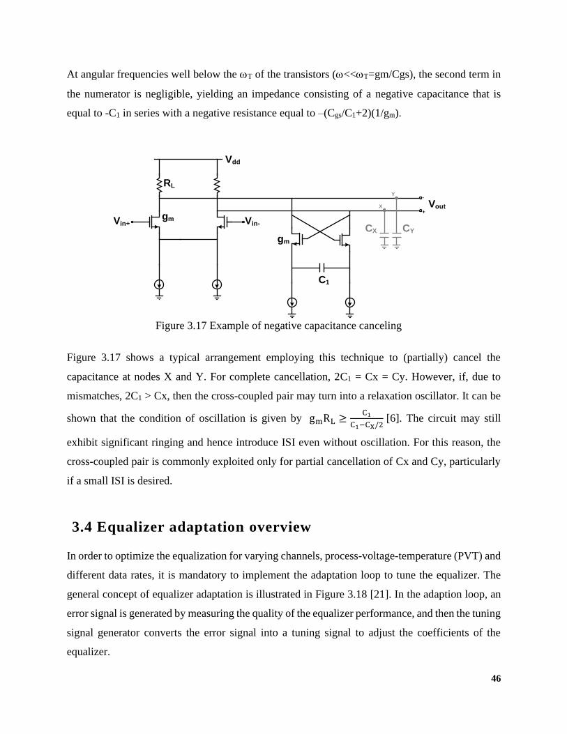
46
At angular frequencies well below the T of the transistors (<<T=gm/Cgs), the second term in
the numerator is negligible, yielding an impedance consisting of a negative capacitance that is
equal to -C1 in series with a negative resistance equal to –(Cgs/C1+2)(1/gm).
Figure 3.17 shows a typical arrangement employing this technique to (partially) cancel the
capacitance at nodes X and Y. For complete cancellation, 2C1 = Cx = Cy. However, if, due to
mismatches, 2C1 > Cx, then the cross-coupled pair may turn into a relaxation oscillator. It can be
shown that the condition of oscillation is given by gmRL ≥C1
C1−CX/2 [6]. The circuit may still
exhibit significant ringing and hence introduce ISI even without oscillation. For this reason, the
cross-coupled pair is commonly exploited only for partial cancellation of Cx and Cy, particularly
if a small ISI is desired.
3.4 Equalizer adaptation overview
In order to optimize the equalization for varying channels, process-voltage-temperature (PVT) and
different data rates, it is mandatory to implement the adaptation loop to tune the equalizer. The
general concept of equalizer adaptation is illustrated in Figure 3.18 [21]. In the adaption loop, an
error signal is generated by measuring the quality of the equalizer performance, and then the tuning
signal generator converts the error signal into a tuning signal to adjust the coefficients of the
equalizer.
Figure 3.17 Example of negative capacitance canceling
Vin+ Vin-gm
Vdd
Vout
RL
gm
CX
-
+
CY
C1
X
Y
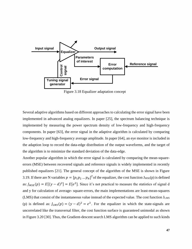
47
Several adaptive algorithms based on different approaches to calculating the error signal have been
implemented in advanced analog equalizers. In paper [25], the spectrum balancing technique is
implemented by measuring the power spectrum density of low-frequency and high-frequency
components. In paper [63], the error signal in the adaptive algorithm is calculated by comparing
low-frequency and high-frequency average amplitude. In paper [64], an eye monitor is included in
the adaption loop to record the data-edge distribution of the output waveforms, and the target of
the algorithm is to minimize the standard deviation of the data-edge.
Another popular algorithm in which the error signal is calculated by comparing the mean-square-
errors (MSE) between recovered signals and reference signals is widely implemented in recently
published equalizers [21]. The general concept of the algorithm of the MSE is shown in Figure
3.19. If there are N variables 𝑝 = [𝑝1𝑝2…𝑝𝑁]𝑇of the equalizer, the cost function JMSE(p) is defined
as: 𝐽𝑀𝑆𝐸(𝑝) = 𝐸[(𝑦 − 𝑑)2] = 𝐸[𝑒2]. Since it’s not practical to measure the statistics of signal d
and y for calculation of average- square-errors, the main implementations are least-mean-squares
(LMS) that consist of the instantaneous value instead of the expected value. The cost function JLMS
(p) is defined as: 𝐽𝐿𝑀𝑆(𝑝) = (𝑦 − 𝑑)2 = 𝑒2 . For the equalizer in which the state-signals are
uncorrelated like the transversal filter, the cost function surface is guaranteed unimodal as shown
in Figure 3.20 [30]. Thus, the Gradient-descent search LMS algorithm can be applied to such kinds
Figure 3.18 Equalizer adaptation concept
EqualizerInput signal Output signal
Error
computation
Tuning signal
generator
Co
ntr
ol
sig
nal Reference signal
Parameters
of interest
Error signal
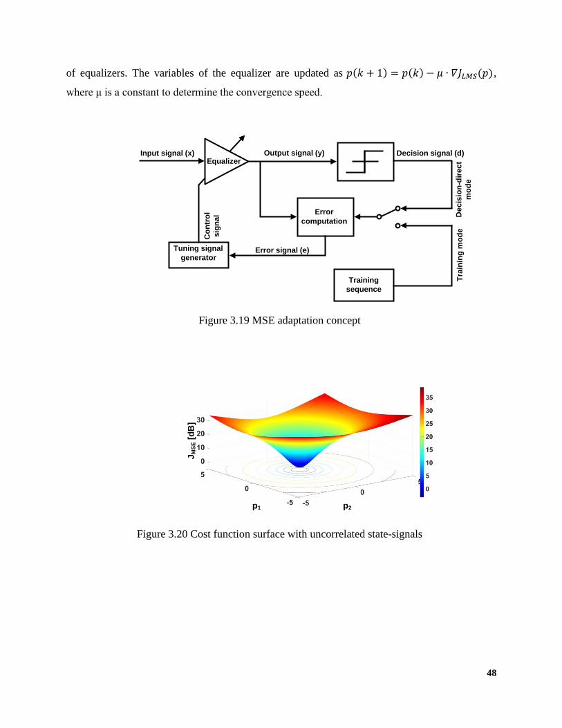
48
of equalizers. The variables of the equalizer are updated as 𝑝(𝑘 + 1) = 𝑝(𝑘) − 𝜇 ∙ 𝛻𝐽𝐿𝑀𝑆(𝑝),
where μ is a constant to determine the convergence speed.
Figure 3.19 MSE adaptation concept
EqualizerInput signal (x) Output signal (y)
Error
computation
Tuning signal
generator
Co
ntr
ol
sig
na
l De
cis
ion
-dir
ec
t
mo
de
Decision signal (d)
Training
sequence
Tra
inin
g m
od
e
Error signal (e)
Figure 3.20 Cost function surface with uncorrelated state-signals
JM
SE [
dB
]
p1 p2
49
Chapter 4 Flexible transversal continuous-time linear
equalizer operating up to 25Gb/s in 28nm CMOS
Abstract
A flexible transversal continuous-time linear equalizer is presented in this chapter. Transceivers
for backplane serial links at 25Gb/s and beyond demand equalizers with high accuracy and
flexibility in matching the channel response. To satisfy the high accuracy requirement, in this
chapter, a very flexible continuous-time linear equalizer (CTLE) with a transversal architecture
is proposed. In chapter 3, the concept to tune gain and zeros separately in a split-path equalizer
have been shown. Similar to such an approach, the proposed equalizer features variable DC gain
and two zeros that can be tuned independently. The transversal architecture makes it compatible
with gradient descent algorithms, allowing optimal adaptation of the gain and zero frequency
locations and improved equalization accuracy. The CTLE was realized in a 28nm CMOS
technology and measurements are presented at data rate from 5Gb/s to 25Gb/s across 20dB-loss
channels. Core power dissipation is 17mW from 1V supply and horizontal eye opening at BER=
10-12 is larger than 50% UI, comparing favorably against previously reported equalizers targeting
similar data-rate and channel loss.
4.1 Introduction
As introduced in chapter 1, the explosive growth of internet traffic, driven by multimedia and
cloud services, continuously pushes for higher bandwidth and aggressive scaling of I/Os for
high-speed electrical links. Ensuring link reliability and low power consumption are key design
targets in view of the increased I/O densities on the same chip. Recent standards have been
introduced to support NRZ signaling with data-rate up to 25-28 Gb/s and transceivers built-in
advanced CMOS technology nodes have been demonstrated [20, 23]. At this speed, typical
backplanes of few tens of cm length introduce a channel loss in excess of 30dB at Nyquist
frequency, and improvement in channel equalization is mandatory as a consequence of the large
inter-symbol interference (ISI). Equalizers must be flexible, operating at variable speed over
different channels, and continuously adapted to counteract environmental drifts (temperature and
humidity) responsible for a slowly varying channel transfer function. The common practice at
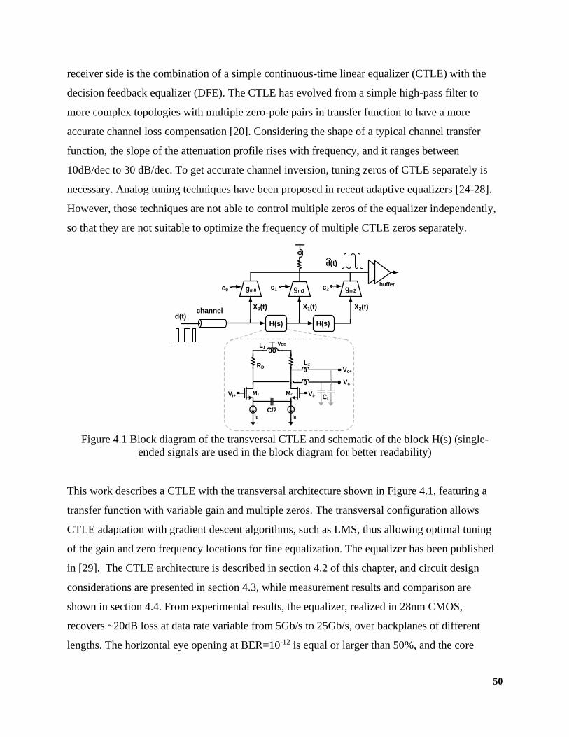
50
receiver side is the combination of a simple continuous-time linear equalizer (CTLE) with the
decision feedback equalizer (DFE). The CTLE has evolved from a simple high-pass filter to
more complex topologies with multiple zero-pole pairs in transfer function to have a more
accurate channel loss compensation [20]. Considering the shape of a typical channel transfer
function, the slope of the attenuation profile rises with frequency, and it ranges between
10dB/dec to 30 dB/dec. To get accurate channel inversion, tuning zeros of CTLE separately is
necessary. Analog tuning techniques have been proposed in recent adaptive equalizers [24-28].
However, those techniques are not able to control multiple zeros of the equalizer independently,
so that they are not suitable to optimize the frequency of multiple CTLE zeros separately.
This work describes a CTLE with the transversal architecture shown in Figure 4.1, featuring a
transfer function with variable gain and multiple zeros. The transversal configuration allows
CTLE adaptation with gradient descent algorithms, such as LMS, thus allowing optimal tuning
of the gain and zero frequency locations for fine equalization. The equalizer has been published
in [29]. The CTLE architecture is described in section 4.2 of this chapter, and circuit design
considerations are presented in section 4.3, while measurement results and comparison are
shown in section 4.4. From experimental results, the equalizer, realized in 28nm CMOS,
recovers ~20dB loss at data rate variable from 5Gb/s to 25Gb/s, over backplanes of different
lengths. The horizontal eye opening at BER=10-12 is equal or larger than 50%, and the core
Figure 4.1 Block diagram of the transversal CTLE and schematic of the block H(s) (single-
ended signals are used in the block diagram for better readability)
H(s)
X0(t) X1(t) X2(t)
d(t)channel
RD
M1 M2
C/2IB
Vi+
Vo+
VDD
IB
L1
L2
c0
d(t)
c1 c2
H(s)
Vi-
Vo-
gm0 gm1 gm2
buffer
CL
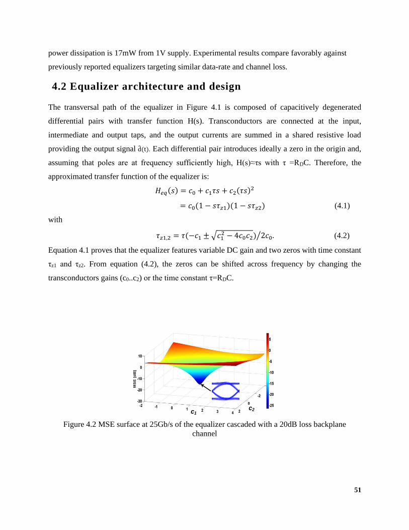
51
power dissipation is 17mW from 1V supply. Experimental results compare favorably against
previously reported equalizers targeting similar data-rate and channel loss.
4.2 Equalizer architecture and design
The transversal path of the equalizer in Figure 4.1 is composed of capacitively degenerated
differential pairs with transfer function H(s). Transconductors are connected at the input,
intermediate and output taps, and the output currents are summed in a shared resistive load
providing the output signal d̂(t). Each differential pair introduces ideally a zero in the origin and,
assuming that poles are at frequency sufficiently high, H(s)≈τs with τ =RDC. Therefore, the
approximated transfer function of the equalizer is:
𝐻𝑒𝑞(𝑠) = 𝑐0 + 𝑐1𝜏𝑠 + 𝑐2(𝜏𝑠)2
= 𝑐0(1 − 𝑠𝜏𝑧1)(1 − 𝑠𝜏𝑧2) (4.1)
with
𝜏𝑧1,2 = 𝜏(−𝑐1 ±√𝑐12 − 4𝑐0𝑐2) 2𝑐0⁄ . (4.2)
Equation 4.1 proves that the equalizer features variable DC gain and two zeros with time constant
τz1 and τz2. From equation (4.2), the zeros can be shifted across frequency by changing the
transconductors gains (c0..c2) or the time constant τ=RDC.
Figure 4.2 MSE surface at 25Gb/s of the equalizer cascaded with a 20dB loss backplane
channel
D1D2c2c1
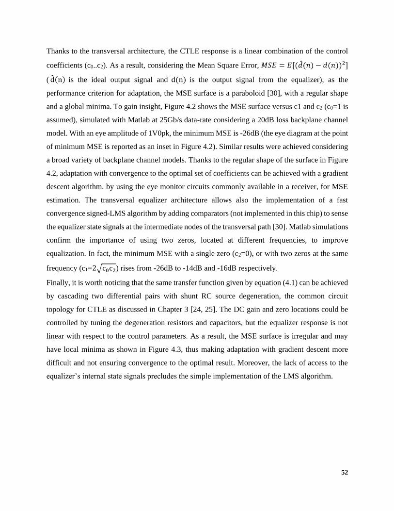
52
Thanks to the transversal architecture, the CTLE response is a linear combination of the control
coefficients (c0..c2). As a result, considering the Mean Square Error, 𝑀𝑆𝐸 = 𝐸[(�̂�(𝑛) − 𝑑(𝑛))2]
( d̂(n) is the ideal output signal and d(n) is the output signal from the equalizer), as the
performance criterion for adaptation, the MSE surface is a paraboloid [30], with a regular shape
and a global minima. To gain insight, Figure 4.2 shows the MSE surface versus c1 and c2 (c0=1 is
assumed), simulated with Matlab at 25Gb/s data-rate considering a 20dB loss backplane channel
model. With an eye amplitude of 1V0pk, the minimum MSE is -26dB (the eye diagram at the point
of minimum MSE is reported as an inset in Figure 4.2). Similar results were achieved considering
a broad variety of backplane channel models. Thanks to the regular shape of the surface in Figure
4.2, adaptation with convergence to the optimal set of coefficients can be achieved with a gradient
descent algorithm, by using the eye monitor circuits commonly available in a receiver, for MSE
estimation. The transversal equalizer architecture allows also the implementation of a fast
convergence signed-LMS algorithm by adding comparators (not implemented in this chip) to sense
the equalizer state signals at the intermediate nodes of the transversal path [30]. Matlab simulations
confirm the importance of using two zeros, located at different frequencies, to improve
equalization. In fact, the minimum MSE with a single zero (c2=0), or with two zeros at the same
frequency (c1=2√c0c2) rises from -26dB to -14dB and -16dB respectively.
Finally, it is worth noticing that the same transfer function given by equation (4.1) can be achieved
by cascading two differential pairs with shunt RC source degeneration, the common circuit
topology for CTLE as discussed in Chapter 3 [24, 25]. The DC gain and zero locations could be
controlled by tuning the degeneration resistors and capacitors, but the equalizer response is not
linear with respect to the control parameters. As a result, the MSE surface is irregular and may
have local minima as shown in Figure 4.3, thus making adaptation with gradient descent more
difficult and not ensuring convergence to the optimal result. Moreover, the lack of access to the
equalizer’s internal state signals precludes the simple implementation of the LMS algorithm.
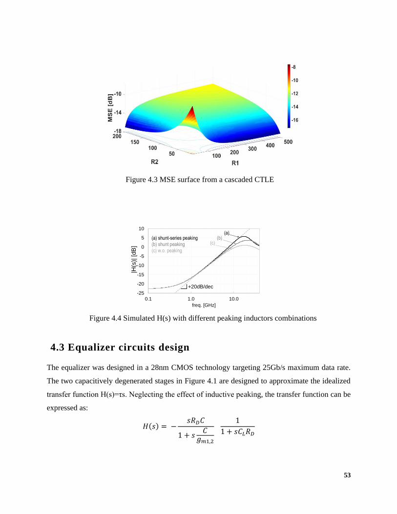
53
4.3 Equalizer circuits design
The equalizer was designed in a 28nm CMOS technology targeting 25Gb/s maximum data rate.
The two capacitively degenerated stages in Figure 4.1 are designed to approximate the idealized
transfer function H(s)=τs. Neglecting the effect of inductive peaking, the transfer function can be
expressed as:
𝐻(𝑠) = −𝑠𝑅𝐷𝐶
1 + 𝑠𝐶
𝑔𝑚1,2
1
1 + 𝑠𝐶𝐿𝑅𝐷
Figure 4.3 MSE surface from a cascaded CTLE
Figure 4.4 Simulated H(s) with different peaking inductors combinations
-25
-20
-15
-10
-5
0
5
10
0.1 1.0 10.0
|H(s
)| [
dB
]
freq. [GHz]
+20dB/dec
(a) shunt-series peaking
(b) shunt peaking
(c) w.o. peaking
(a) (b)
(c)
|H(s
)| [dB
]
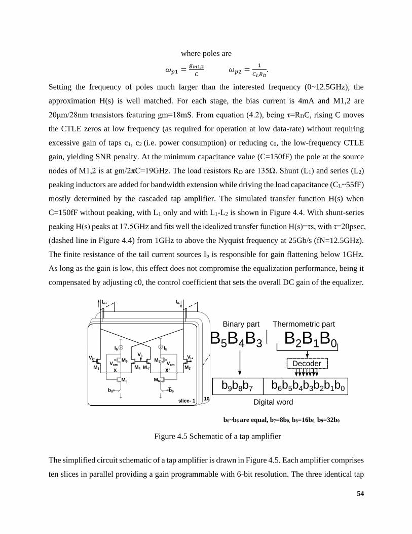
54
where poles are
𝜔𝑝1 =𝑔𝑚1,2
𝐶 𝜔𝑝2 =
1
𝐶𝐿𝑅𝐷.
Setting the frequency of poles much larger than the interested frequency (0~12.5GHz), the
approximation H(s) is well matched. For each stage, the bias current is 4mA and M1,2 are
20μm/28nm transistors featuring gm=18mS. From equation (4.2), being τ=RDC, rising C moves
the CTLE zeros at low frequency (as required for operation at low data-rate) without requiring
excessive gain of taps c1, c2 (i.e. power consumption) or reducing c0, the low-frequency CTLE
gain, yielding SNR penalty. At the minimum capacitance value (C=150fF) the pole at the source
nodes of M1,2 is at gm/2πC=19GHz. The load resistors RD are 135Ω. Shunt (L1) and series (L2)
peaking inductors are added for bandwidth extension while driving the load capacitance (CL~55fF)
mostly determined by the cascaded tap amplifier. The simulated transfer function H(s) when
C=150fF without peaking, with L1 only and with L1-L2 is shown in Figure 4.4. With shunt-series
peaking H(s) peaks at 17.5GHz and fits well the idealized transfer function H(s)=τs, with τ=20psec,
(dashed line in Figure 4.4) from 1GHz to above the Nyquist frequency at 25Gb/s (fN=12.5GHz).
The finite resistance of the tail current sources Ib is responsible for gain flattening below 1GHz.
As long as the gain is low, this effect does not compromise the equalization performance, being it
compensated by adjusting c0, the control coefficient that sets the overall DC gain of the equalizer.
The simplified circuit schematic of a tap amplifier is drawn in Figure 4.5. Each amplifier comprises
ten slices in parallel providing a gain programmable with 6-bit resolution. The three identical tap
b0~b6 are equal, b7=8b0, b8=16b0, b9=32b0
Figure 4.5 Schematic of a tap amplifier
Vi+ Vi+
b0b0
Vi-
Io+ Io-
slice- 1 10
Ib Ib
Vcm Vcm
M5
M6
M4'
M6'
M3 M4
M5'
M3'X X’
B5B4B3 B2B1B0
Binary part Thermometric part
b6b5b4b3b2b1b0
Decoder
b9b8b7
Digital word
55
amplifiers (gm0, gm1, gm2 in Figure 4.1) are connected to the same load to control the gain. To ensure
gain monotonicity with respect to the digital control code, essential for adaptation, a combination
of binary- and thermometric-weighted slices are used. The circuit in each slice is made of two
differential transconductors (M3,4 and M3’,4’) driven by the same input signals but delivering
currents with opposite sign, allowing the overall gain to span from negative to positive values.
The linearity of a traditional differential pair is poor due to the fixed tail current source. A pseudo-
differential pair has better linearity without removing the limit set by the constant biasing current
source, but requires a proper circuit for setting the bias point independently from the input
common-mode. Based on this, a class-AB pseudo-differential pair with a flipped-voltage follower
is proposed. Transistors M5,5’ are biased at the gate with the common mode of the input signal
(sensed at the center tap of a resistive divider, not shown) and together with M6,6’ form flipped
voltage followers forcing low impedance at the common source nodes X, X’. In this way M3,4 and
M3’,4’ work as Class-AB pseudo-differential pairs, featuring enhanced linearity. The flipped-
voltage follower provides better sourcing capability and keeps the common source node more
stable than using a simpler common drain transistor as shown in Figure 4.6b. This is proved by the
simulated transfer characteristic in Figure 4.7 for the 3 transconductors in Figure 4.6. The flipped
voltage follower transconductor has twice the linear range than a simple differential pair, at the
same quiescent current, leading to an input 1dB compression point near 1Vpk-pk. In this way the
equalizer can withstand large input swing with low distortion, thus preserving high SNR when
recovering large channel loss. The quiescent current consumption of each tap amplifier is 3mA
and maximum gain is 14mS.
The output currents from the three-tap amplifiers in the equalizer are summed in a shared load,
realized with resistors and shunt peaking inductors for bandwidth extension. The equalizer is
followed by a programmable-gain two-stage buffer to drive the instruments for experimental
characterization.
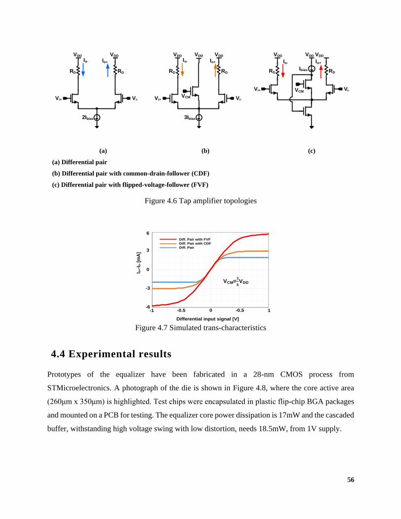
56
4.4 Experimental results
Prototypes of the equalizer have been fabricated in a 28-nm CMOS process from
STMicroelectronics. A photograph of the die is shown in Figure 4.8, where the core active area
(260μm x 350μm) is highlighted. Test chips were encapsulated in plastic flip-chip BGA packages
and mounted on a PCB for testing. The equalizer core power dissipation is 17mW and the cascaded
buffer, withstanding high voltage swing with low distortion, needs 18.5mW, from 1V supply.
(a) (b) (c)
(a) Differential pair
(b) Differential pair with common-drain-follower (CDF)
(c) Differential pair with flipped-voltage-follower (FVF)
Figure 4.6 Tap amplifier topologies
Vi+ Vi-VCM
IbiasRD RD
Io- Io+
Vi+ Vi-
RD RD
Io- Io+
2Ibias
Vi+ Vi-
RD RD
Io- Io+
3Ibias
VCM
VDD VDD VDD VDDVDD VDD VDDVDD
Figure 4.7 Simulated trans-characteristics
-6.E-03
-3.E-03
0.E+00
3.E-03
6.E-03
-0.5 -0.25 0 0.25 0.5
Title
Differential input signal [V]
-1
I o+-I
o- [m
A]
-0.5 0 1-0.5
3
6
0
-3
-6
Diff. Pair with FVF
Diff. Pair with CDF
Diff. Pair
VCM=
VDD
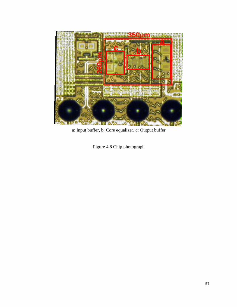
57
a: Input buffer, b: Core equalizer, c: Output buffer
Figure 4.8 Chip photograph
26
0µ
m
350µm
ca
b
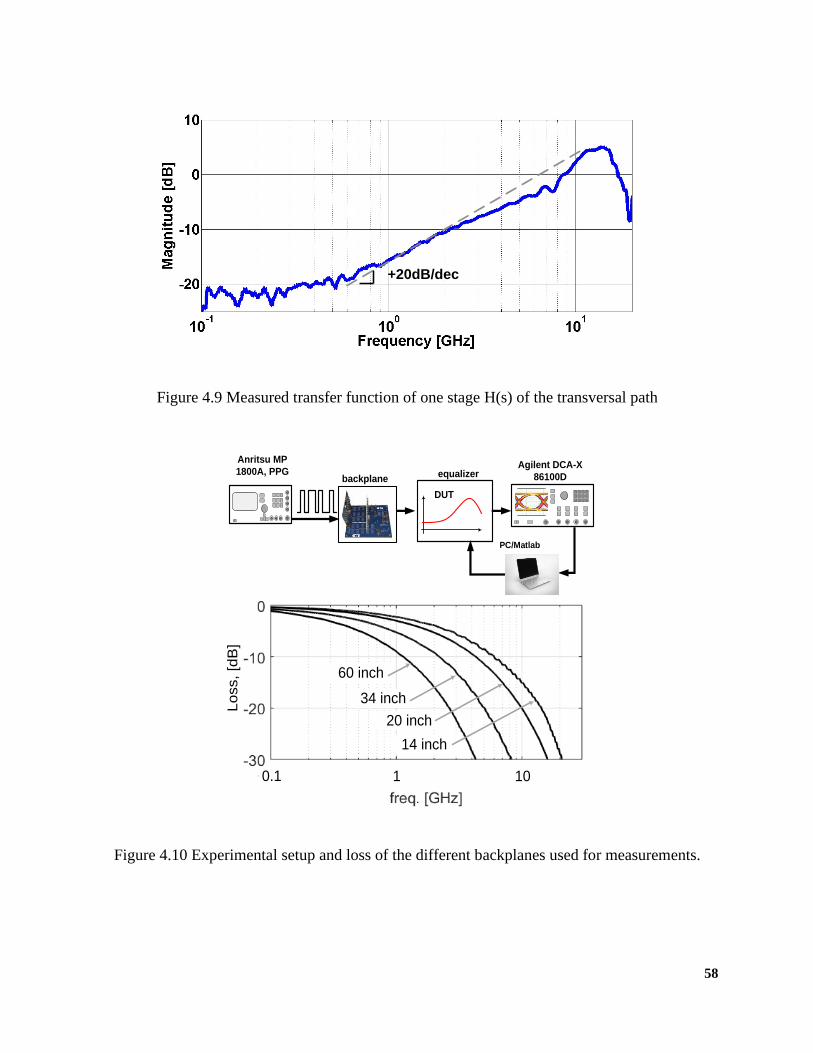
58
Figure 4.9 Measured transfer function of one stage H(s) of the transversal path
Figure 4.10 Experimental setup and loss of the different backplanes used for measurements.
+20dB/dec
0.1 1 10
equalizer
Anritsu MP
1800A, PPG backplane
DUT
Agilent DCA-X
86100D
PC/Matlab
Loss,
[dB
]
60 inch
34 inch
20 inch
14 inch
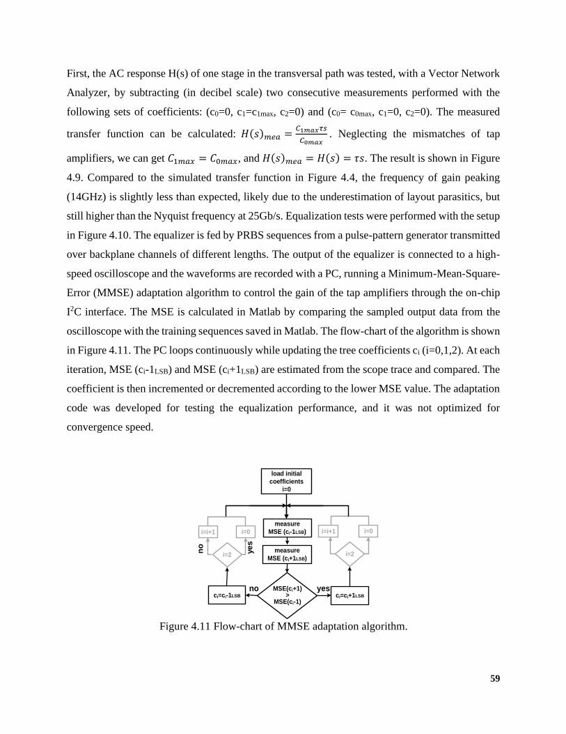
59
First, the AC response H(s) of one stage in the transversal path was tested, with a Vector Network
Analyzer, by subtracting (in decibel scale) two consecutive measurements performed with the
following sets of coefficients: (c0=0, c1=c1max, c2=0) and (c0= c0max, c1=0, c2=0). The measured
transfer function can be calculated: 𝐻(𝑠)𝑚𝑒𝑎 =𝐶1𝑚𝑎𝑥𝜏𝑠
𝐶0𝑚𝑎𝑥. Neglecting the mismatches of tap
amplifiers, we can get 𝐶1𝑚𝑎𝑥 = 𝐶0𝑚𝑎𝑥, and 𝐻(𝑠)𝑚𝑒𝑎 = 𝐻(𝑠) = 𝜏𝑠. The result is shown in Figure
4.9. Compared to the simulated transfer function in Figure 4.4, the frequency of gain peaking
(14GHz) is slightly less than expected, likely due to the underestimation of layout parasitics, but
still higher than the Nyquist frequency at 25Gb/s. Equalization tests were performed with the setup
in Figure 4.10. The equalizer is fed by PRBS sequences from a pulse-pattern generator transmitted
over backplane channels of different lengths. The output of the equalizer is connected to a high-
speed oscilloscope and the waveforms are recorded with a PC, running a Minimum-Mean-Square-
Error (MMSE) adaptation algorithm to control the gain of the tap amplifiers through the on-chip
I2C interface. The MSE is calculated in Matlab by comparing the sampled output data from the
oscilloscope with the training sequences saved in Matlab. The flow-chart of the algorithm is shown
in Figure 4.11. The PC loops continuously while updating the tree coefficients ci (i=0,1,2). At each
iteration, MSE (ci-1LSB) and MSE (ci+1LSB) are estimated from the scope trace and compared. The
coefficient is then incremented or decremented according to the lower MSE value. The adaptation
code was developed for testing the equalization performance, and it was not optimized for
convergence speed.
Figure 4.11 Flow-chart of MMSE adaptation algorithm.
no
yes
load initial
coefficients
i=0
measure
MSE (ci-1LSB)
ci=ci+1LSB
measure
MSE (ci+1LSB)
MSE(ci+1)>
MSE(ci-1)
i=i+1
i=2
i=0
ci=ci-1LSB
yesno
i=i+1
i=2
i=0
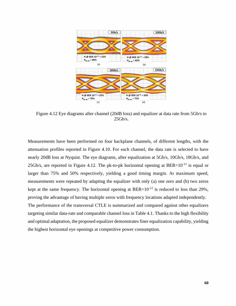
60
Measurements have been performed on four backplane channels, of different lengths, with the
attenuation profiles reported in Figure 4.10. For each channel, the data rate is selected to have
nearly 20dB loss at Nyquist. The eye diagrams, after equalization at 5Gb/s, 10Gb/s, 18Gb/s, and
25Gb/s, are reported in Figure 4.12. The pk-to-pk horizontal opening at BER=10-12 is equal or
larger than 75% and 50% respectively, yielding a good timing margin. At maximum speed,
measurements were repeated by adapting the equalizer with only (a) one zero and (b) two zeros
kept at the same frequency. The horizontal opening at BER=10-12 is reduced to less than 29%,
proving the advantage of having multiple zeros with frequency locations adapted independently.
The performance of the transversal CTLE is summarized and compared against other equalizers
targeting similar data-rate and comparable channel loss in Table 4.1. Thanks to the high flexibility
and optimal adaptation, the proposed equalizer demonstrates finer equalization capability, yielding
the highest horizontal eye openings at competitive power consumption.
Figure 4.12 Eye diagrams after channel (20dB loss) and equalizer at data rate from 5Gb/s to
25Gb/s.
(a) (b)
(c) (d)
5Gb/s 10Gb/s
18Gb/s 25Gb/s
H @ BER 10-12 = 52%Hpk-pk = 86%
H @ BER 10-12 = 58%Hpk-pk = 82%
H @ BER 10-12 = 55%Hpk-pk = 76%
H @ BER 10-12 = 50%Hpk-pk = 75%
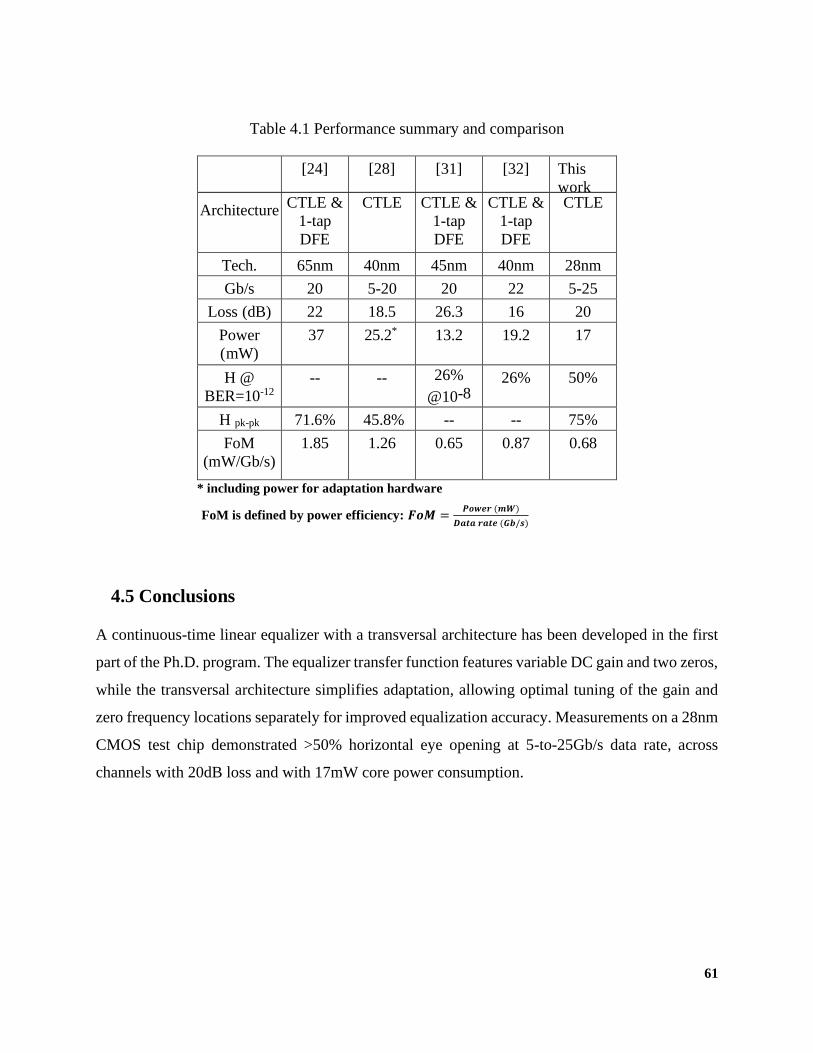
61
4.5 Conclusions
A continuous-time linear equalizer with a transversal architecture has been developed in the first
part of the Ph.D. program. The equalizer transfer function features variable DC gain and two zeros,
while the transversal architecture simplifies adaptation, allowing optimal tuning of the gain and
zero frequency locations separately for improved equalization accuracy. Measurements on a 28nm
CMOS test chip demonstrated >50% horizontal eye opening at 5-to-25Gb/s data rate, across
channels with 20dB loss and with 17mW core power consumption.
Table 4.1 Performance summary and comparison
[24] [28] [31] [32] This
work
Architecture CTLE &
1-tap
DFE
CTLE CTLE &
1-tap
DFE
CTLE &
1-tap
DFE
CTLE
Tech. 65nm 40nm 45nm 40nm 28nm
Gb/s 20 5-20 20 22 5-25
Loss (dB) 22 18.5 26.3 16 20
Power
(mW) 37 25.2* 13.2 19.2 17
H @
BER=10-12
-- -- 26%
@10-8
26% 50%
H pk-pk 71.6% 45.8% -- -- 75%
FoM
(mW/Gb/s)
1.85 1.26 0.65 0.87 0.68
* including power for adaptation hardware
FoM is defined by power efficiency: 𝑭𝒐𝑴 =𝑷𝒐𝒘𝒆𝒓 (𝒎𝑾)
𝑫𝒂𝒕𝒂 𝒓𝒂𝒕𝒆 (𝑮𝒃/𝒔)
62
Chapter 5 PAM-4 analog front-end for 64Gb/s transceiver in
28nm CMOS FDSOI
Abstract
A PAM-4 analog front-end for a transceiver operating up to 64Gb/s in 28nm CMOS FDSOI,
tailored to short-reach electrical links is presented. The analog front-end includes variable-gain-
amplifiers (VGAs), and flexible CTLE with low, mid and high frequency channel loss compensation.
The VGA combines two different topologies that give high linearity and flat frequency response.
The receiver equalization is based only on the flexible CTLE which proves a very accurate channel
inversion through a transfer function that can be optimally adapted at low, mid and high frequency
independently. The CTLE meets the performance requirements of CEI-56G-VSR without requiring
DFE implementation. As a result, timing constraints for comparators in data and edge sampling
paths may be relaxed by using track-and-hold stages, saving power consumption. The full
transceiver (TX, RX and clock generation) operates from 16Gb/s to 64Gb/s in PAM-4 and 8Gb/s
to 32Gb/s in NRZ. A TX-to-RX link at 64Gb/s, across a 16.8dB-loss channel reaches 10-12 minimum
BER and 0.19UI horizontal eye opening at BER=10-6, with 5.02mW/Gb/s power dissipation.
5.1 Introduction
The constant growth of digitally intensive services, such as the Internet of Things (IoT),
multimedia on demand, cloud storage and cloud computing, is driving the continuous upgrade of
telecommunication infrastructures and data-centers to support an exponential network traffic
increase. New standards for electrical interconnects, addressing the need for higher communication
speed, introduced PAM-4 in the migration path from 28Gb/s per lane to 56Gb/s and beyond
(112Gb/s projects are currently in progress) [33].
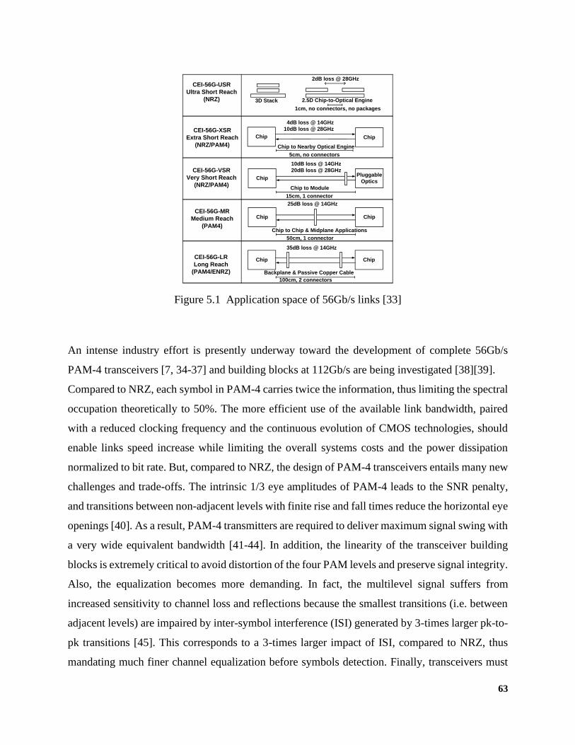
63
An intense industry effort is presently underway toward the development of complete 56Gb/s
PAM-4 transceivers [7, 34-37] and building blocks at 112Gb/s are being investigated [38][39].
Compared to NRZ, each symbol in PAM-4 carries twice the information, thus limiting the spectral
occupation theoretically to 50%. The more efficient use of the available link bandwidth, paired
with a reduced clocking frequency and the continuous evolution of CMOS technologies, should
enable links speed increase while limiting the overall systems costs and the power dissipation
normalized to bit rate. But, compared to NRZ, the design of PAM-4 transceivers entails many new
challenges and trade-offs. The intrinsic 1/3 eye amplitudes of PAM-4 leads to the SNR penalty,
and transitions between non-adjacent levels with finite rise and fall times reduce the horizontal eye
openings [40]. As a result, PAM-4 transmitters are required to deliver maximum signal swing with
a very wide equivalent bandwidth [41-44]. In addition, the linearity of the transceiver building
blocks is extremely critical to avoid distortion of the four PAM levels and preserve signal integrity.
Also, the equalization becomes more demanding. In fact, the multilevel signal suffers from
increased sensitivity to channel loss and reflections because the smallest transitions (i.e. between
adjacent levels) are impaired by inter-symbol interference (ISI) generated by 3-times larger pk-to-
pk transitions [45]. This corresponds to a 3-times larger impact of ISI, compared to NRZ, thus
mandating much finer channel equalization before symbols detection. Finally, transceivers must
Figure 5.1 Application space of 56Gb/s links [33]
3D Stack 2.5D Chip-to-Optical Engine
2dB loss @ 28GHz
1cm, no connectors, no packages
Chip Chip
Chip to Nearby Optical Engine
4dB loss @ 14GHz
10dB loss @ 28GHz
5cm, no connectors
ChipPluggable
Optics
Chip to Module
15cm, 1 connector
10dB loss @ 14GHz
20dB loss @ 28GHz
Chip Chip
Chip to Chip & Midplane Applications
50cm, 1 connector
25dB loss @ 14GHz
Chip Chip
Backplane & Passive Copper Cable
100cm, 2 connectors
35dB loss @ 14GHz
CEI-56G-USR
Ultra Short Reach
(NRZ)
CEI-56G-XSR
Extra Short Reach
(NRZ/PAM4)
CEI-56G-VSR
Very Short Reach
(NRZ/PAM4)
CEI-56G-MR
Medium Reach
(PAM4)
CEI-56G-LR
Long Reach
(PAM4/ENRZ)
64
comply with legacy components, supporting a wide interval of data-rates and NRZ signaling at
reduced speed, still maintaining power efficiency.
The application space envisioned for 56Gb/s electrical interfaces is depicted in Figure 5.1. Very
different scenarios are considered, from ultra-short links between chips mounted within the same
package, with negligible interconnect loss and reflections, up to long-reach links where the
electrical interface must cope with up to 1mt-long channels (either backplane or cable) and the
severe reflections generated by multiple packages and connectors. The harsh operating condition
of long-reach links is driving the migration toward ADC-based receivers, where complex and
flexible equalization and symbol detection are performed by digital signal processing (DSP) [46-
48]. 56Gb/s PAM-4 receivers, implemented in state-of-the-art 16nm FinFet technology,
demonstrated operation over 30-35dB channel loss at 14GHz Nyquist frequency, with a
normalized power consumption (excluding the DSP power) in the range 4.4-6.6mW/Gb/s
[7][36][37]. Considering the DSP power, the total RX power consumption reported in [37] is above
8mW/Gb/s. To improve the energy efficiency over links with reduced channel loss and reflections,
e.g. in medium- or very-short-reach links for chip-to-chip or chip-to-module interconnects (Figure
5.1), power scalable ADC-based receivers have been proposed [36][37]. But for such applications,
analog PAM-4 receivers may offer higher power and area saving [41][49]. A main limiting factor
to the efficiency of analog receivers is the implementation of the decision feedback equalizer
(DFE). PAM-4 requires hardware triplication and improved resolution, compared to NRZ, rising
challenges to satisfy critical DFE feedback timing at low power also with advanced CMOS
technology nodes [41].
In this chapter, a PAM-4 analog front-end for transceiver operating up to 64Gb/s is presented. The
CTLE of the analog front-end features a transfer function optimally adapted at low, mid, and high
frequency, allowing to meet the performance requirements of CEI-56G-VSR scenario with margin.
Not requiring DFE, relaxed timing constraints allow implementing data, edge and eye monitor
detection with track-and-hold stages, drastically reducing the power requirements. At 64Gb/s the
full receiver requires 180mW from a single 1V supply, corresponding to 2.8mW/Gb/s only. The
full transceiver operates from 16Gb/s to 64Gb/s in PAM-4 and from 8Gb/s to 32Gb/s in NRZ. A
TX-to-RX link at 64Gb/s across a 16.8dB-loss channel proves 10-12 minimum BER and 0.19UI
horizontal eye opening at BER=10-6, with 5.02mW/Gb/s power dissipation (comprising RX, TX
and clocks generation).
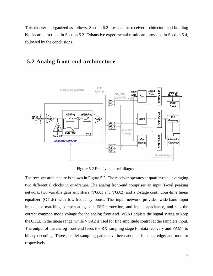
65
This chapter is organized as follows. Section 5.2 presents the receiver architecture and building
blocks are described in Section 5.3. Exhaustive experimental results are provided in Section 5.4,
followed by the conclusions.
5.2 Analog front-end architecture
The receiver architecture is shown in Figure 5.2. The receiver operates at quarter-rate, leveraging
two differential clocks in quadrature. The analog front-end comprises an input T-coil peaking
network, two variable gain amplifiers (VGA1 and VGA2) and a 2-stage continuous-time linear
equalizer (CTLE) with low-frequency boost. The input network provides wide-band input
impedance matching compensating pad, ESD protection, and input capacitance, and sets the
correct common mode voltage for the analog front-end. VGA1 adjusts the signal swing to keep
the CTLE in the linear range, while VGA2 is used for fine amplitude control at the samplers input.
The output of the analog front-end feeds the RX sampling stage for data recovery and PAM4 to
binary decoding. Three parallel sampling paths have been adopted for data, edge, and monitor
respectively.
Figure 5.2 Receivers block diagram
MID Freq
LOW Freq
HIGH Freq RX In
Data
CLK
Recovery
Adaptation
Controller
Data Out40MSB+40LSB
Edge
Eye
MonitorANALOG FRONT-END
CTLE
PIs & DCD
control
PRBS
Check
LP
BK
From TX
CLK
8-phases
VGA2
DE
MU
X 4
:40
CKIP, CKINCKQP,CKQN
VGA1
Input
Data
Output
Data
CLK
Threshold Set
From clocks generator
DE
MU
X 4
:40
DE
MU
X 4
:40
DC
DD
CD
DC
DD
CD
DC
DD
CD
66
Since the receiver operates at quarter-rate, after data sampling, thermometer to binary decoders
provide 4MSB+4LSB NRZ streams, further parallelized by 4:40 demultiplexers. Data path outputs
are also used by the clock recovery unit, in combination with the outputs of the edge path, to set
the optimal clock sampling phase. Early-late information for the second-order clock-recovery,
driving the Phase Interpolators, is derived after demultiplexers, allowing selective removal of
undesired PAM4 transitions in the digital domain. The undesired PAM4 transitions are from
simultaneous LSB/MSB transitions. Those transitions have undesired timing distributions at the
LSB comparator threshold [40]. Furthermore, data path outputs are used by the adaptation
controller, in combination with measurements performed through the eye monitor path, to
implement the digital calibration engine. Specifically, the integrated eye monitor builds PAM-4
signal statistics for adaptation of the samplers’ thresholds, VGA gains, and CTLE frequency
response. Finally, data path outputs are used by the integrated PRBS BER checker. Offsets in the
analog front-end and in each comparator are calibrated with dedicated autozeroing routines at start-
up.
Details of the most critical stages in the analog front-end, i.e. VGAs and CTLE, and of the
sampling stages are provided in the next subsection.
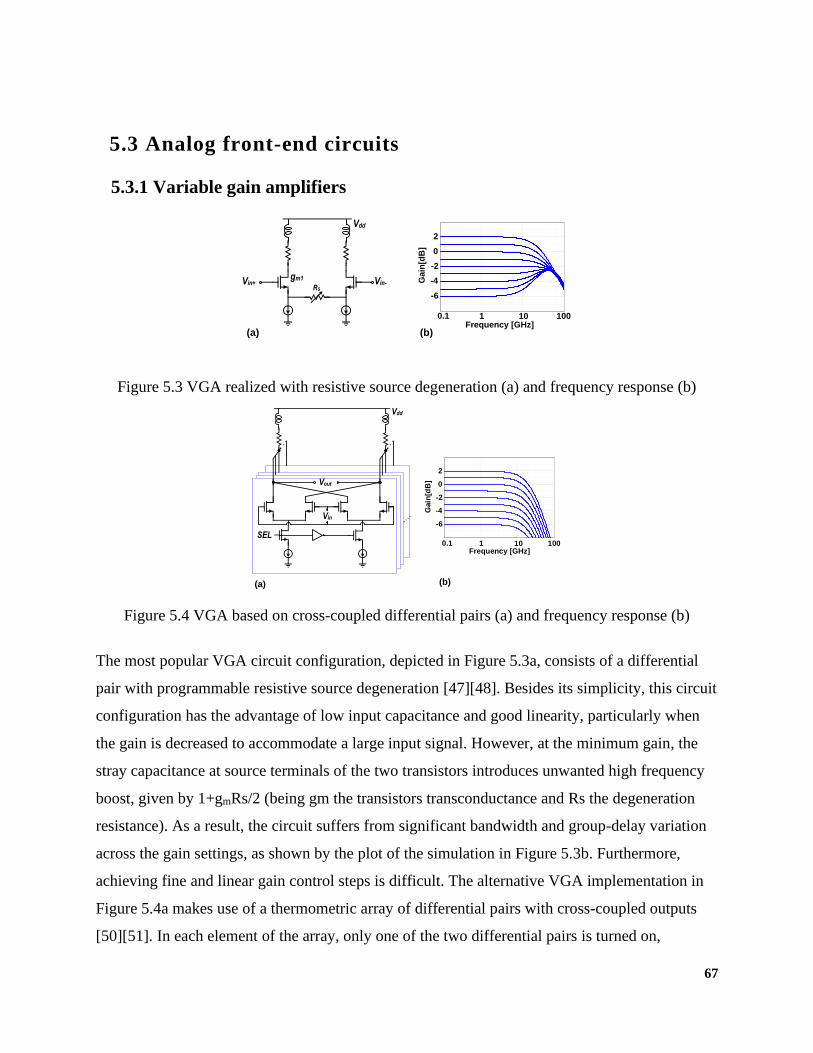
67
5.3 Analog front-end circuits
5.3.1 Variable gain amplifiers
The most popular VGA circuit configuration, depicted in Figure 5.3a, consists of a differential
pair with programmable resistive source degeneration [47][48]. Besides its simplicity, this circuit
configuration has the advantage of low input capacitance and good linearity, particularly when
the gain is decreased to accommodate a large input signal. However, at the minimum gain, the
stray capacitance at source terminals of the two transistors introduces unwanted high frequency
boost, given by 1+gmRs/2 (being gm the transistors transconductance and Rs the degeneration
resistance). As a result, the circuit suffers from significant bandwidth and group-delay variation
across the gain settings, as shown by the plot of the simulation in Figure 5.3b. Furthermore,
achieving fine and linear gain control steps is difficult. The alternative VGA implementation in
Figure 5.4a makes use of a thermometric array of differential pairs with cross-coupled outputs
[50][51]. In each element of the array, only one of the two differential pairs is turned on,
Figure 5.3 VGA realized with resistive source degeneration (a) and frequency response (b)
Figure 5.4 VGA based on cross-coupled differential pairs (a) and frequency response (b)
Vin+ Vin-RS
gm1
Vdd
-8
-6
-4
-2
0
2
4
1E+08 1E+09 1E+10 1E+11
Ga
in [
dB
]
Frequency [Hz]
2
0
-2
-4
-6
Ga
in[d
B]
Frequency [GHz]0.1 1 10 100
(a) (b)
-8
-6
-4
-2
0
2
4
1E+08 1E+09 1E+10 1E+11
Gain
[d
B]
Frequency [Hz]
2
0
-2
-4
-6
Gain
[dB
]
Frequency [GHz]0.1 1 10 100
(b)
Vin
SEL
Vdd
(a)
Vout
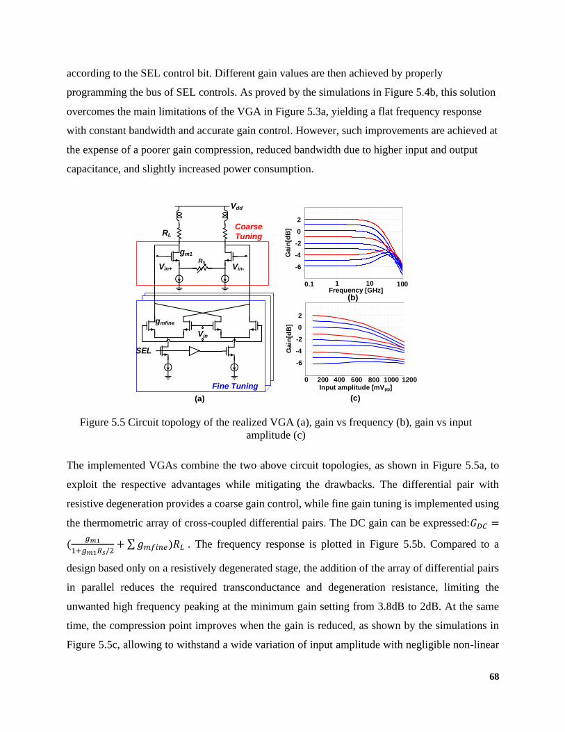
68
according to the SEL control bit. Different gain values are then achieved by properly
programming the bus of SEL controls. As proved by the simulations in Figure 5.4b, this solution
overcomes the main limitations of the VGA in Figure 5.3a, yielding a flat frequency response
with constant bandwidth and accurate gain control. However, such improvements are achieved at
the expense of a poorer gain compression, reduced bandwidth due to higher input and output
capacitance, and slightly increased power consumption.
The implemented VGAs combine the two above circuit topologies, as shown in Figure 5.5a, to
exploit the respective advantages while mitigating the drawbacks. The differential pair with
resistive degeneration provides a coarse gain control, while fine gain tuning is implemented using
the thermometric array of cross-coupled differential pairs. The DC gain can be expressed:𝐺𝐷𝐶 =
(𝑔𝑚1
1+𝑔𝑚1𝑅𝑠/2+ ∑𝑔𝑚𝑓𝑖𝑛𝑒)𝑅𝐿 . The frequency response is plotted in Figure 5.5b. Compared to a
design based only on a resistively degenerated stage, the addition of the array of differential pairs
in parallel reduces the required transconductance and degeneration resistance, limiting the
unwanted high frequency peaking at the minimum gain setting from 3.8dB to 2dB. At the same
time, the compression point improves when the gain is reduced, as shown by the simulations in
Figure 5.5c, allowing to withstand a wide variation of input amplitude with negligible non-linear
Figure 5.5 Circuit topology of the realized VGA (a), gain vs frequency (b), gain vs input
amplitude (c)
Vin
SEL
Vin+ Vin-
RS
gm1
Vdd
Fine Tuning
Coarse
Tuning
-8
-6
-4
-2
0
2
4
1E+08 1E+09 1E+10 1E+11
Gain
[d
B]
Frequency [Hz]
Frequency [GHz]0.1 1 10 100
2
0
-2
-4
-6
Gain
[dB
]
-8
-6
-4
-2
0
2
4
0 200 400 600 800 1000 1200
Gain
[d
B]
Input [mVppd]
2
0
-2
-4
-6
Gain
[dB
]
200 400 600 800 1000 12000Input amplitude [mVpp]
(a)
(b)
(c)
gmfine
RL
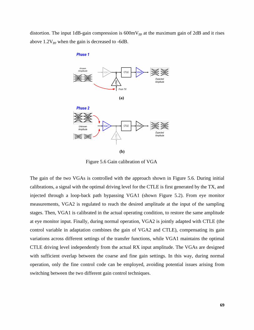
69
distortion. The input 1dB-gain compression is 600mVpp at the maximum gain of 2dB and it rises
above 1.2Vpp when the gain is decreased to -6dB.
The gain of the two VGAs is controlled with the approach shown in Figure 5.6. During initial
calibrations, a signal with the optimal driving level for the CTLE is first generated by the TX, and
injected through a loop-back path bypassing VGA1 (shown Figure 5.2). From eye monitor
measurements, VGA2 is regulated to reach the desired amplitude at the input of the sampling
stages. Then, VGA1 is calibrated in the actual operating condition, to restore the same amplitude
at eye monitor input. Finally, during normal operation, VGA2 is jointly adapted with CTLE (the
control variable in adaptation combines the gain of VGA2 and CTLE), compensating its gain
variations across different settings of the transfer functions, while VGA1 maintains the optimal
CTLE driving level independently from the actual RX input amplitude. The VGAs are designed
with sufficient overlap between the coarse and fine gain settings. In this way, during normal
operation, only the fine control code can be employed, avoiding potential issues arising from
switching between the two different gain control techniques.
(a)
(b)
Figure 5.6 Gain calibration of VGA
CTLE
LPB
K
VGA2
Expected
Amplitude
Phase 1
Known
AmplitudeVGA1
From TX
VGA1 CTLE
LPB
K
VGA2Unknown
Amplitude
Expected
Amplitude
Phase 2
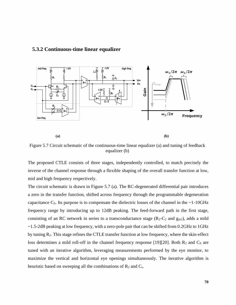
70
5.3.2 Continuous-time linear equalizer
The proposed CTLE consists of three stages, independently controlled, to match precisely the
inverse of the channel response through a flexible shaping of the overall transfer function at low,
mid and high frequency respectively.
The circuit schematic is drawn in Figure 5.7 (a). The RC-degenerated differential pair introduces
a zero in the transfer function, shifted across frequency through the programmable degeneration
capacitance CS. Its purpose is to compensate the dielectric losses of the channel in the ~1-10GHz
frequency range by introducing up to 12dB peaking. The feed-forward path in the first stage,
consisting of an RC network in series to a transconductance stage (R2-C2 and gm2), adds a mild
~1.5-2dB peaking at low frequency, with a zero-pole pair that can be shifted from 0.2GHz to 1GHz
by tuning R2. This stage refines the CTLE transfer function at low frequency, where the skin-effect
loss determines a mild roll-off in the channel frequency response [19][20]. Both R2 and CS are
tuned with an iterative algorithm, leveraging measurements performed by the eye monitor, to
maximize the vertical and horizontal eye openings simultaneously. The iterative algorithm is
heuristic based on sweeping all the combinations of R2 and Cs.
(a) (b)
Figure 5.7 Circuit schematic of the continuous-time linear equalizer (a) and tuning of feedback
equalizer (b)
mid freq.
low freq.
Vin+
Vo-
Vo+
high freq.
gm2+-
+-
Vin-
gm3+-
+
-
gm5+-
+
-gm4
RS
CS
R2
C2
gm1
R1 R3
RF
CF /2
1.0V
+-
+
-
Cp
1.0V 1.0V
L3
Gloop
Gain
Frequency /𝟐
/𝟐 𝟐/𝟐
71
The last stage of the CTLE, implemented with a feedback topology, introduces additional high-
frequency boost (up to 6dB) to finely recover the steep roll-off of the channel profile close to
Nyquist frequency. Neglecting the shunt peaking inductor L3, circuit analysis yields the following
transfer function, from the input of gm3 to the output of the CTLE:
𝐻𝐻𝐹(𝜔) =𝑔𝑚3𝑅3
1+𝐺𝐿𝑂𝑂𝑃
(1+𝑗𝜔
𝜔𝑓)
(1+𝑗𝜔
𝜔1)(1+𝑗
𝜔
𝜔2) (5.1)
where GLOOP=gm5R3gm4RF is the static loop gain and f=1/RFCF. The two poles 1,2 in equation
(5.1) are given by:
𝜔1,2 =𝜔𝑓+𝜔𝑝±√𝜔𝑓
2+𝜔𝑝2−2𝜔𝑓𝜔𝑝(1+2𝐺𝐿𝑂𝑂𝑃)
2 (5.2)
with p =1/R3CP the angular frequency of the parasitic pole at the output nodes of gm3. To ensure
stability with a wide margin, and to minimize distortion due to excessive group-delay variation,
the stage is designed to operate with loop gain low enough such that, from (5.2), 1,2 are real. In
this condition, the dependence from GLOOP of (5.2) can be linearly approximated, yielding:
𝜔1 ≈ 𝜔𝑓 (1 +𝜔𝑝
𝜔𝑝−𝜔𝑓𝐺𝐿𝑂𝑂𝑃)
𝜔2 ≈ 𝜔𝑝 (1 +𝜔𝑝
𝜔𝑝−𝜔𝑓𝐺𝐿𝑂𝑂𝑃)
(5.3)
From (5.1) and (5.3), the peaking of the stage, i.e. max(|HHF()|/|HHF(−0)|), is controlled by
GLOOP reducing the low-frequency gain and by pushing the two poles to higher frequency.
Assuming that p is sufficiently high, such that 2 >> 1, max(|HHF()|/|HHF(−0)|) = 1+GLOOP.
The main advantage of the feedback topology is that the position of the zero in HHF() is constant.
As a result, a very selective control of the CTLE transfer function can be achieved through GLOOP
at high frequency with negligible impact at low and mid-frequency, greatly simplifying the CTLE
adaptation. The tuning of feedback equalizer is plotted in Figure 5.7 (b). The variation of low-
frequency gain, leading to variation of the output eye amplitude, is compensated by VGA2 after
the CTLE. Moreover, the feedback topology allows HHF() to be continuously adapted with a
Least Mean Squares algorithm, during normal RX operation, by taking the CTLE output signal as
gradient information and using the eye monitor for error slicing [30].
The equalization accuracy of the proposed CTLE is demonstrated through simulations considering
an openly available reference channel for 56Gb/s short-reach links [52] in Figure 5.8. Simulations
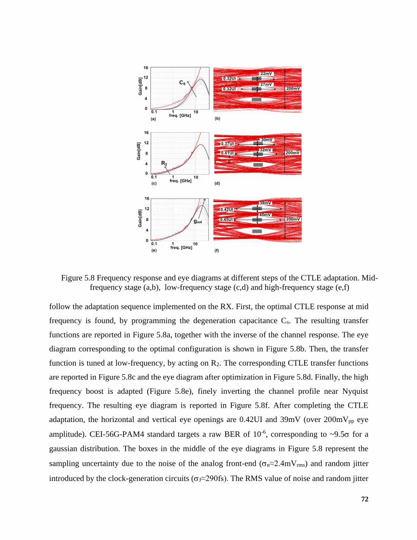
72
follow the adaptation sequence implemented on the RX. First, the optimal CTLE response at mid
frequency is found, by programming the degeneration capacitance Cs. The resulting transfer
functions are reported in Figure 5.8a, together with the inverse of the channel response. The eye
diagram corresponding to the optimal configuration is shown in Figure 5.8b. Then, the transfer
function is tuned at low-frequency, by acting on R2. The corresponding CTLE transfer functions
are reported in Figure 5.8c and the eye diagram after optimization in Figure 5.8d. Finally, the high
frequency boost is adapted (Figure 5.8e), finely inverting the channel profile near Nyquist
frequency. The resulting eye diagram is reported in Figure 5.8f. After completing the CTLE
adaptation, the horizontal and vertical eye openings are 0.42UI and 39mV (over 200mVpp eye
amplitude). CEI-56G-PAM4 standard targets a raw BER of 10-6, corresponding to ~9.5 for a
gaussian distribution. The boxes in the middle of the eye diagrams in Figure 5.8 represent the
sampling uncertainty due to the noise of the analog front-end (n≈2.4mVrms) and random jitter
introduced by the clock-generation circuits (J≈290fs). The RMS value of noise and random jitter
Figure 5.8 Frequency response and eye diagrams at different steps of the CTLE adaptation. Mid-
frequency stage (a,b), low-frequency stage (c,d) and high-frequency stage (e,f)
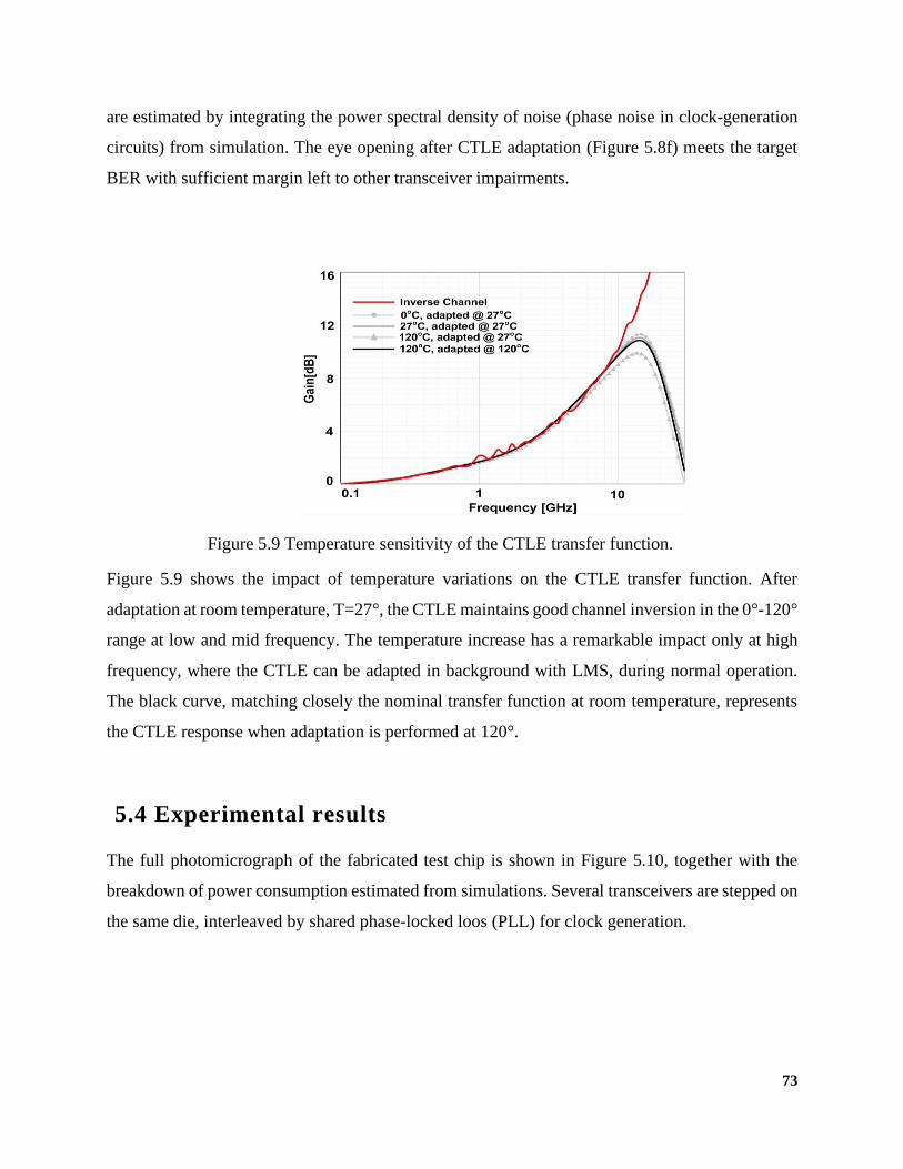
73
are estimated by integrating the power spectral density of noise (phase noise in clock-generation
circuits) from simulation. The eye opening after CTLE adaptation (Figure 5.8f) meets the target
BER with sufficient margin left to other transceiver impairments.
Figure 5.9 shows the impact of temperature variations on the CTLE transfer function. After
adaptation at room temperature, T=27°, the CTLE maintains good channel inversion in the 0°-120°
range at low and mid frequency. The temperature increase has a remarkable impact only at high
frequency, where the CTLE can be adapted in background with LMS, during normal operation.
The black curve, matching closely the nominal transfer function at room temperature, represents
the CTLE response when adaptation is performed at 120°.
5.4 Experimental results
The full photomicrograph of the fabricated test chip is shown in Figure 5.10, together with the
breakdown of power consumption estimated from simulations. Several transceivers are stepped on
the same die, interleaved by shared phase-locked loos (PLL) for clock generation.
Figure 5.9 Temperature sensitivity of the CTLE transfer function.
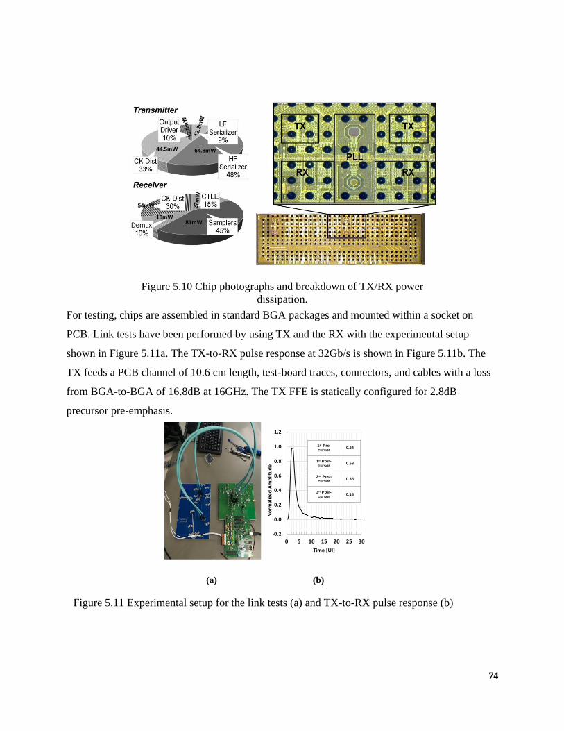
74
For testing, chips are assembled in standard BGA packages and mounted within a socket on
PCB. Link tests have been performed by using TX and the RX with the experimental setup
shown in Figure 5.11a. The TX-to-RX pulse response at 32Gb/s is shown in Figure 5.11b. The
TX feeds a PCB channel of 10.6 cm length, test-board traces, connectors, and cables with a loss
from BGA-to-BGA of 16.8dB at 16GHz. The TX FFE is statically configured for 2.8dB
precursor pre-emphasis.
Figure 5.10 Chip photographs and breakdown of TX/RX power
dissipation.
44.5mW 64.8mW
54mW
81mW18mW
(a) (b)
Figure 5.11 Experimental setup for the link tests (a) and TX-to-RX pulse response (b)
-0.2
0.0
0.2
0.4
0.6
0.8
1.0
1.2
0 5 10 15 20 25 30
No
rmal
ize
d A
mp
litu
de
Time [UI]
(a) (b)
1st Pre-cursor
0.24
1st Post-cursor
0.58
2nd Post-cursor
0.36
3rd Post-cursor
0.14
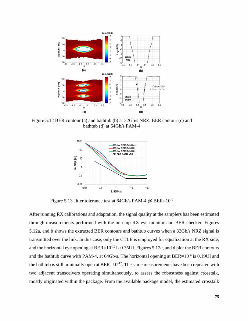
75
After running RX calibrations and adaptation, the signal quality at the samplers has been estimated
through measurements performed with the on-chip RX eye monitor and BER checker. Figures
5.12a, and b shows the extracted BER contours and bathtub curves when a 32Gb/s NRZ signal is
transmitted over the link. In this case, only the CTLE is employed for equalization at the RX side,
and the horizontal eye opening at BER=10-12 is 0.35UI. Figures 5.12c, and d plot the BER contours
and the bathtub curve with PAM-4, at 64Gb/s. The horizontal opening at BER=10-6 is 0.19UI and
the bathtub is still minimally open at BER=10-12. The same measurements have been repeated with
two adjacent transceivers operating simultaneously, to assess the robustness against crosstalk,
mostly originated within the package. From the available package model, the estimated crosstalk
Figure 5.12 BER contour (a) and bathtub (b) at 32Gb/s NRZ. BER contour (c) and
bathtub (d) at 64Gb/s PAM-4
Figure 5.13 Jitter tolerance test at 64Gb/s PAM-4 @ BER=10-6
0.01
0.1
1
10
100
1000
0.01 0.1 1 10 100
SJ
amp
l [U
I]
SJ f[MHz]
RX Jtol CDR GainMaxRX Jtol CDR GainMidRX Jtol CDR GainMinCEI 56G PAM4 VSR
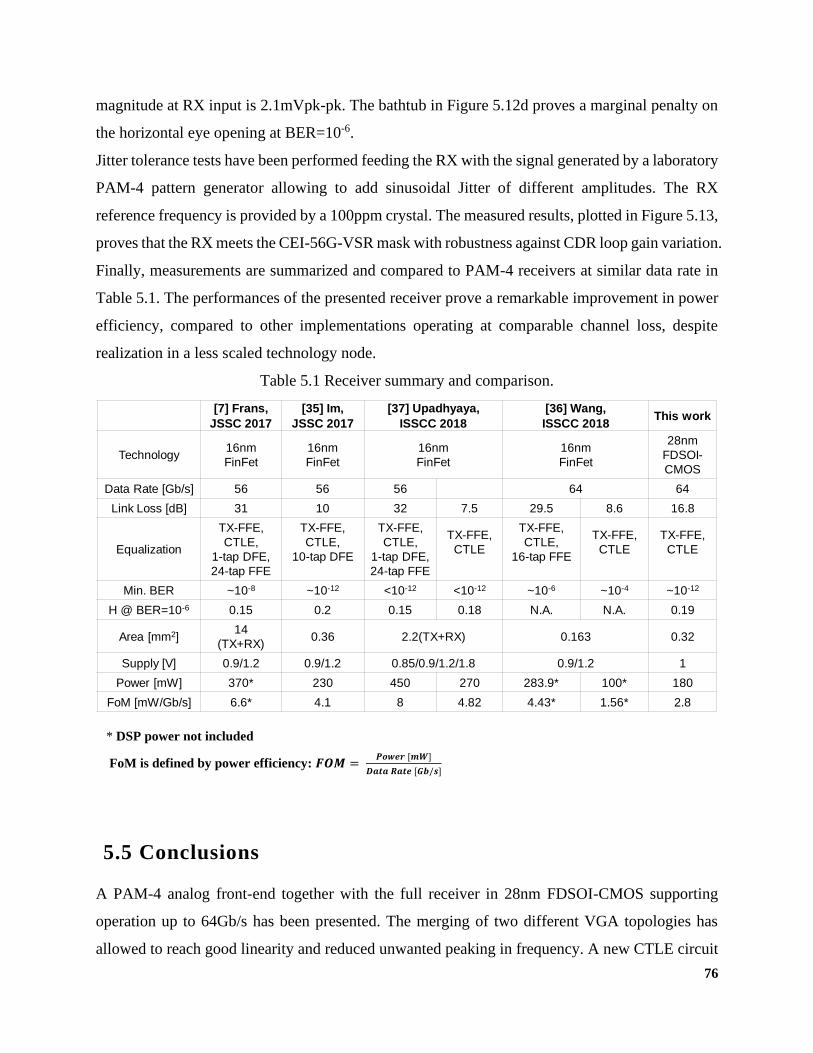
76
magnitude at RX input is 2.1mVpk-pk. The bathtub in Figure 5.12d proves a marginal penalty on
the horizontal eye opening at BER=10-6.
Jitter tolerance tests have been performed feeding the RX with the signal generated by a laboratory
PAM-4 pattern generator allowing to add sinusoidal Jitter of different amplitudes. The RX
reference frequency is provided by a 100ppm crystal. The measured results, plotted in Figure 5.13,
proves that the RX meets the CEI-56G-VSR mask with robustness against CDR loop gain variation.
Finally, measurements are summarized and compared to PAM-4 receivers at similar data rate in
Table 5.1. The performances of the presented receiver prove a remarkable improvement in power
efficiency, compared to other implementations operating at comparable channel loss, despite
realization in a less scaled technology node.
5.5 Conclusions
A PAM-4 analog front-end together with the full receiver in 28nm FDSOI-CMOS supporting
operation up to 64Gb/s has been presented. The merging of two different VGA topologies has
allowed to reach good linearity and reduced unwanted peaking in frequency. A new CTLE circuit
Table 5.1 Receiver summary and comparison.
* DSP power not included
FoM is defined by power efficiency: 𝑭𝑶𝑴 = 𝑷𝒐𝒘𝒆𝒓 [𝒎𝑾]
𝑫𝒂𝒕𝒂 𝑹𝒂𝒕𝒆 [𝑮𝒃/𝒔]
[7] Frans,
JSSC 2017
[35] Im,
JSSC 2017
[37] Upadhyaya,
ISSCC 2018
[36] Wang,
ISSCC 2018This work
Technology16nm
FinFet
16nm
FinFet
16nm
FinFet
16nm
FinFet
28nm
FDSOI-
CMOS
Data Rate [Gb/s] 56 56 56 64 64
Link Loss [dB] 31 10 32 7.5 29.5 8.6 16.8
Equalization
TX-FFE,
CTLE,
1-tap DFE,
24-tap FFE
TX-FFE,
CTLE,
10-tap DFE
TX-FFE,
CTLE,
1-tap DFE,
24-tap FFE
TX-FFE,
CTLE
TX-FFE,
CTLE,
16-tap FFE
TX-FFE,
CTLE
TX-FFE,
CTLE
Min. BER ~10-8 ~10-12 <10-12 <10-12 ~10-6 ~10-4 ~10-12
H @ BER=10-6 0.15 0.2 0.15 0.18 N.A. N.A. 0.19
Area [mm2]14
(TX+RX)0.36 2.2(TX+RX) 0.163 0.32
Supply [V] 0.9/1.2 0.9/1.2 0.85/0.9/1.2/1.8 0.9/1.2 1
Power [mW] 370* 230 450 270 283.9* 100* 180
FoM [mW/Gb/s] 6.6* 4.1 8 4.82 4.43* 1.56* 2.8

77
topology, featuring high flexibility and accuracy to match the channel response has been proposed.
The CTLE meets the equalization requirements of CEI-56G-VSR links with margin, allowing the
implementation of a mostly-analog RX, without DFE, thus saving significant power consumption.
At 64 Gb/s, a TX-to-RX link over 16.8dB-loss channel reaches 10-6 BER with a 0.19UI timing
margin, requiring only 2.8mW/Gb/s for the full receiver.
78
Chapter 6 PAM-4 analog front-end for 112Gb/s receiver in
7nm FinFet
Abstract
The analog front-end for a PAM-4 receiver operating up to 112Gb/s in 7nm FinFet is presented
in this chapter. It comprises a variable-gain-amplifier (VGA) and a flexible CTLE with low, mid
and high frequency channel-loss compensation, followed by a buffer. Particular care was paid to
design high linearity circuits, a key aspect to maintain PAM-4 signal integrity with the low supply
voltage of 0.9V, constrained by the adopted technology. T-coil peaking and capacitance
neutralization are exploited in CTLE to extend the operation frequency above 28GHz. The analog
front-end can be used for short reach link or long reach link when merged with an ADC-based
receiver back end. Simulations are performed with a reference channel (Synectic channel)
featuring 15dB loss at Nyquist frequency. The results prove that this analog front-end can
successfully support 112Gb/s PAM signaling.
6.1 Introduction
As presented in Chapter 1, the continuous growth of IP traffic pushes the development of serial
link transceivers supporting higher speed. Recently, 100Gb/s per lane and 400Gb/s in four lanes
physical layers are specified in IEEE 802.3ck Ethernet standards and 112Gb/s serial link
transceivers are being investigated to double the data rate of 56Gb/s transceivers with improved
power efficiency [53]. Digital circuits tremendously benefit from transistor scaling in 16nm or
7nm FinFet technology [54], such that the speed and power dissipation are improved while scaling
the chip area. The development of transceivers combining analog circuits and digital systems may
also take advantage of the higher performance of the digital circuits. However, the consolidated
analog circuits developed in previous nodes, such as 28nm FD SOI, are not guaranteed to work
properly with just scaling in 16nm/7nm FinFet technology due to significant changes in transistor
behavior, new complex layout rules, and modeling techniques [55]. The analog design challenges
in FinFet technology are also raised by lower operating voltages, severe impact of post-layout of
small vias and fins, and a remarkable reduction of the allowed current density in the metal lines.
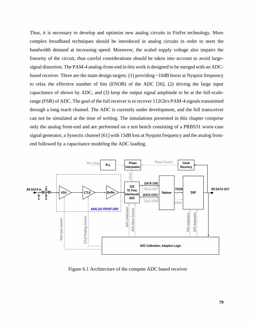
79
Thus, it is necessary to develop and optimize new analog circuits in FinFet technology. More
complex broadband techniques should be introduced in analog circuits in order to meet the
bandwidth demand at increasing speed. Moreover, the scaled supply voltage also impairs the
linearity of the circuit, thus careful considerations should be taken into account to avoid large-
signal distortion. The PAM-4 analog-front-end in this work is designed to be merged with an ADC-
based receiver. Three are the main design targets: (1) providing ~10dB boost at Nyquist frequency
to relax the effective number of bits (ENOB) of the ADC [56], (2) driving the large input
capacitance of shown by ADC, and (3) keep the output signal amplitude to be at the full-scale-
range (FSR) of ADC. The goal of the full receiver is to recover 112Gb/s PAM-4 signals transmitted
through a long reach channel. The ADC is currently under development, and the full transceiver
can not be simulated at the time of writing. The simulations presented in this chapter comprise
only the analog front-end and are performed on a test bench consisting of a PRBS31 worst-case
signal generator, a Synectic channel [61] with 15dB loss at Nyquist frequency and the analog front-
end followed by a capacitance modeling the ADC loading.
Figure 6.1 Architecture of the compete ADC based receiver
RX DATA InBuffer
32X
7b Time
Interleaved
ADC
RX DATA OUT
ADC Calibration, Adaption Logic
DSPRetimer
ANALOG FRONT-END
VGA CTLE
Clo
ck
Phase Control
AD
C C
alib
rati
on
AD
C S
kew
Co
ntr
ol
FF
E A
dap
tati
on
CT
LE
Pea
kin
g C
on
tro
l
VG
A G
ain
Co
ntr
ol
DF
E A
dap
tati
on
Clock
7X32b
PLLPhase
Interpolator
Clock
Recovery
Ref. Clock
DATA CH0
Clock CH0
Clock CH31
DATA CH31
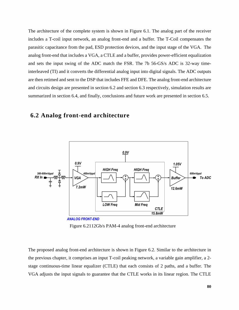
80
The architecture of the complete system is shown in Figure 6.1. The analog part of the receiver
includes a T-coil input network, an analog front-end and a buffer. The T-Coil compensates the
parasitic capacitance from the pad, ESD protection devices, and the input stage of the VGA. The
analog front-end that includes a VGA, a CTLE and a buffer, provides power-efficient equalization
and sets the input swing of the ADC match the FSR. The 7b 56-GS/s ADC is 32-way time-
interleaved (TI) and it converts the differential analog input into digital signals. The ADC outputs
are then retimed and sent to the DSP that includes FFE and DFE. The analog front-end architecture
and circuits design are presented in section 6.2 and section 6.3 respectively, simulation results are
summarized in section 6.4, and finally, conclusions and future work are presented in section 6.5.
6.2 Analog front-end architecture
The proposed analog front-end architecture is shown in Figure 6.2. Similar to the architecture in
the previous chapter, it comprises an input T-coil peaking network, a variable gain amplifier, a 2-
stage continuous-time linear equalizer (CTLE) that each consists of 2 paths, and a buffer. The
VGA adjusts the input signals to guarantee that the CTLE works in its linear region. The CTLE
Figure 6.2112Gb/s PAM-4 analog front-end architecture
HiGH Freq
LOW Freq
HIGH Freq
RX In
ANALOG FRONT-END
CTLE
Buffer
Mid Freq
To ADCVGA
300-600mVppd 400mVppd 600mVppd
1.05V
0.9V
0.9V
15.8mW
12.6mW7.2mW
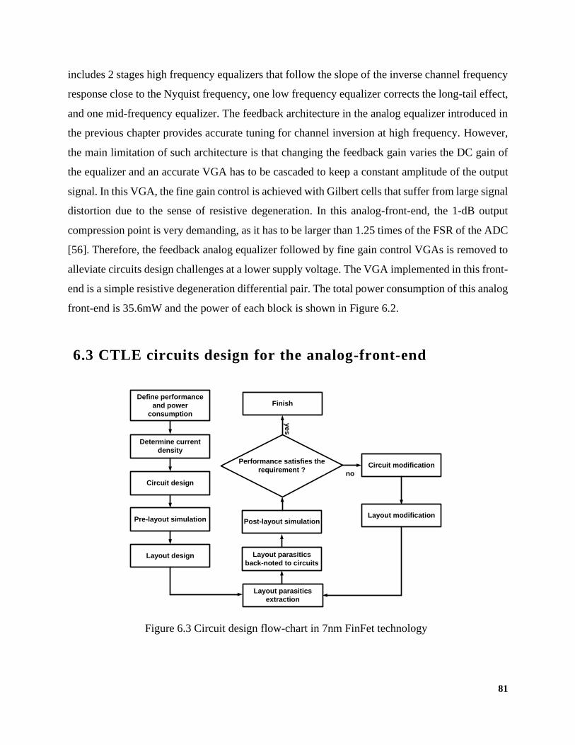
81
includes 2 stages high frequency equalizers that follow the slope of the inverse channel frequency
response close to the Nyquist frequency, one low frequency equalizer corrects the long-tail effect,
and one mid-frequency equalizer. The feedback architecture in the analog equalizer introduced in
the previous chapter provides accurate tuning for channel inversion at high frequency. However,
the main limitation of such architecture is that changing the feedback gain varies the DC gain of
the equalizer and an accurate VGA has to be cascaded to keep a constant amplitude of the output
signal. In this VGA, the fine gain control is achieved with Gilbert cells that suffer from large signal
distortion due to the sense of resistive degeneration. In this analog-front-end, the 1-dB output
compression point is very demanding, as it has to be larger than 1.25 times of the FSR of the ADC
[56]. Therefore, the feedback analog equalizer followed by fine gain control VGAs is removed to
alleviate circuits design challenges at a lower supply voltage. The VGA implemented in this front-
end is a simple resistive degeneration differential pair. The total power consumption of this analog
front-end is 35.6mW and the power of each block is shown in Figure 6.2.
6.3 CTLE circuits design for the analog-front-end
Figure 6.3 Circuit design flow-chart in 7nm FinFet technology
Define performance
and power
consumption
Determine current
density
Circuit design
Pre-layout simulation
Layout design
Layout parasitics
extraction
Layout parasitics
back-noted to circuits
Post-layout simulation
Performance satisfies the
requirement ?Circuit modification
Layout modification
Finish
ye
s
no
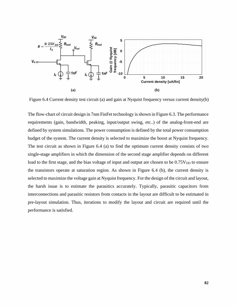
82
The flow-chart of circuit design in 7nm FinFet technology is shown in Figure 6.3. The performance
requirements (gain, bandwidth, peaking, input/output swing, etc..) of the analog-front-end are
defined by system simulations. The power consumption is defined by the total power consumption
budget of the system. The current density is selected to maximize the boost at Nyquist frequency.
The test circuit as shown in Figure 6.4 (a) to find the optimum current density consists of two
single-stage amplifiers in which the dimension of the second stage amplifier depends on different
load to the first stage, and the bias voltage of input and output are chosen to be 0.75VDD to ensure
the transistors operate at saturation region. As shown in Figure 6.4 (b), the current density is
selected to maximize the voltage gain at Nyquist frequency. For the design of the circuit and layout,
the harsh issue is to estimate the parasitics accurately. Typically, parasitic capacitors from
interconnections and parasitic resistors from contacts in the layout are difficult to be estimated in
pre-layout simulation. Thus, iterations to modify the layout and circuit are required until the
performance is satisfied.
(a) (b)
Figure 6.4 Current density test circuit (a) and gain at Nyquist frequency versus current density(b)
Vin
VDD
Rload
VDD
Vout
Rload
Ib Ib1nF 1nF
𝑹 = .𝟐 𝑽𝑫𝑫
𝒃
Gain
@ N
yq
uis
t
fre
qu
en
cy [
dB
]
Current density [uA/fin]
5
0
-5
-10-10.00
-5.00
0.00
5.00
0 5 10 15 20
Tit
le
Title0 5 10 15 20
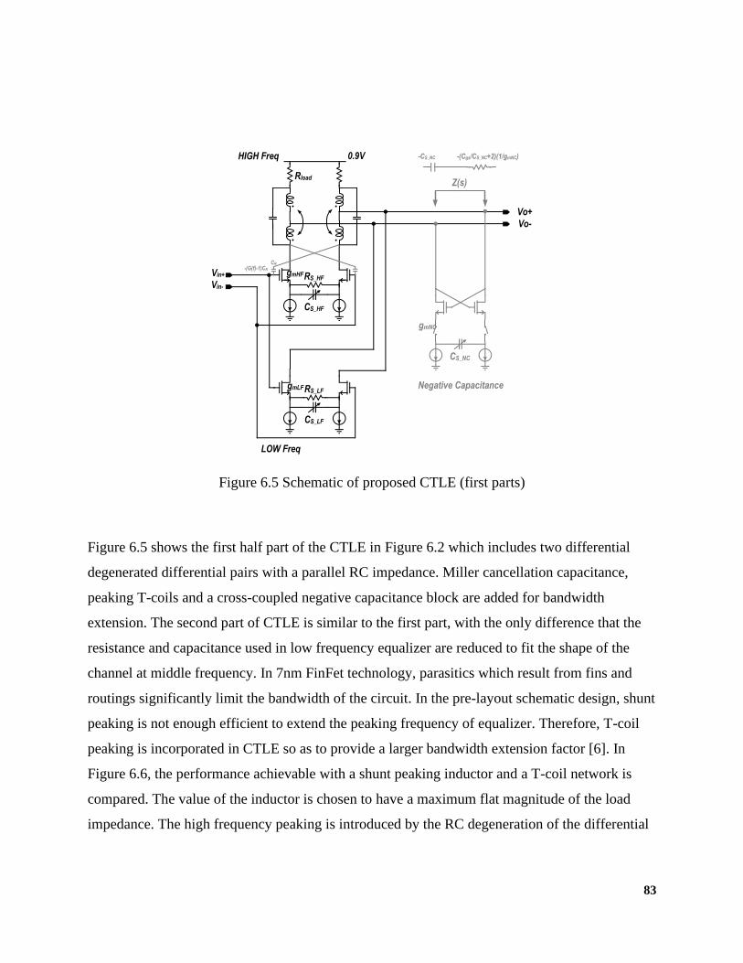
83
Figure 6.5 shows the first half part of the CTLE in Figure 6.2 which includes two differential
degenerated differential pairs with a parallel RC impedance. Miller cancellation capacitance,
peaking T-coils and a cross-coupled negative capacitance block are added for bandwidth
extension. The second part of CTLE is similar to the first part, with the only difference that the
resistance and capacitance used in low frequency equalizer are reduced to fit the shape of the
channel at middle frequency. In 7nm FinFet technology, parasitics which result from fins and
routings significantly limit the bandwidth of the circuit. In the pre-layout schematic design, shunt
peaking is not enough efficient to extend the peaking frequency of equalizer. Therefore, T-coil
peaking is incorporated in CTLE so as to provide a larger bandwidth extension factor [6]. In
Figure 6.6, the performance achievable with a shunt peaking inductor and a T-coil network is
compared. The value of the inductor is chosen to have a maximum flat magnitude of the load
impedance. The high frequency peaking is introduced by the RC degeneration of the differential
Figure 6.5 Schematic of proposed CTLE (first parts)
HIGH Freq
Vin+
Vin-
RS_HF
CS_HF
gmHF
Rload
0.9V
RS_LF
CS_LF
gmLF
CS_NC
gmNC
Vo-
Vo+
LOW Freq
Negative Capacitance
-CS_NC -(Cgs/CS_NC+2)(1/gmNC)
Z(s)
-(G(f)-1)CN
CN
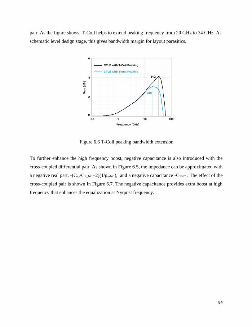
84
pair. As the figure shows, T-Coil helps to extend peaking frequency from 20 GHz to 34 GHz. At
schematic level design stage, this gives bandwidth margin for layout parasitics.
To further enhance the high frequency boost, negative capacitance is also introduced with the
cross-coupled differential pair. As shown in Figure 6.5, the impedance can be approximated with
a negative real part, -(Cgs/CS_NC+2)(1/gmNC), and a negative capacitance -CSNC . The effect of the
cross-coupled pair is shown In Figure 6.7. The negative capacitance provides extra boost at high
frequency that enhances the equalization at Nyquist frequency.
Figure 6.6 T-Coil peaking bandwidth extension
0
2
4
6
1E+08 1E+09 1E+10 1E+11
Tit
le
TitleFrequency [GHz]
0.1 1 10
0
4
6
100
Ga
in [
dB
]
2
20G
34G
CTLE with T-Coil Peaking
CTLE with Shunt Peaking
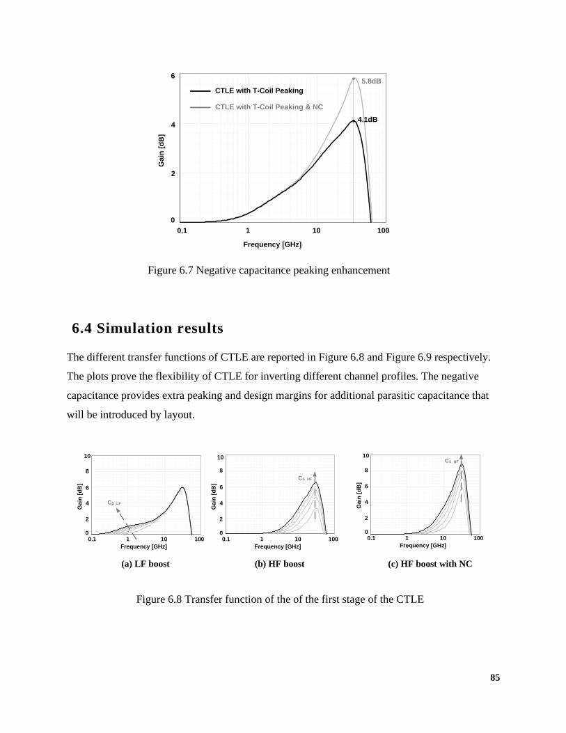
85
6.4 Simulation results
The different transfer functions of CTLE are reported in Figure 6.8 and Figure 6.9 respectively.
The plots prove the flexibility of CTLE for inverting different channel profiles. The negative
capacitance provides extra peaking and design margins for additional parasitic capacitance that
will be introduced by layout.
Figure 6.7 Negative capacitance peaking enhancement
0
2
4
6
1E+08 1E+09 1E+10 1E+11
Tit
le
TitleFrequency [GHz]
0.1 1 10
0
4
6
100
Ga
in [
dB
]
CTLE with T-Coil Peaking
CTLE with T-Coil Peaking & NC
5.8dB
4.1dB
2
(a) LF boost (b) HF boost (c) HF boost with NC
Figure 6.8 Transfer function of the of the first stage of the CTLE
Frequency [GHz]
0.1 1 10
2
4
6
8
100
Ga
in [
dB
]
00
2
4
6
8
10
1E+08 1E+09 1E+10 1E+11
Tit
le
Title
10
0
2
4
6
8
10
1E+08 1E+09 1E+10 1E+11
Tit
le
Title
Frequency [GHz]
0.1 1 10
2
4
6
8
100
Ga
in [
dB
]
0
10
0
2
4
6
8
10
1E+08 1E+09 1E+10 1E+11
Tit
le
TitleFrequency [GHz]
0.1 1 10
2
4
6
8
100
Ga
in [
dB
]
0
10
CS_LF
CS_HF
CS_HF
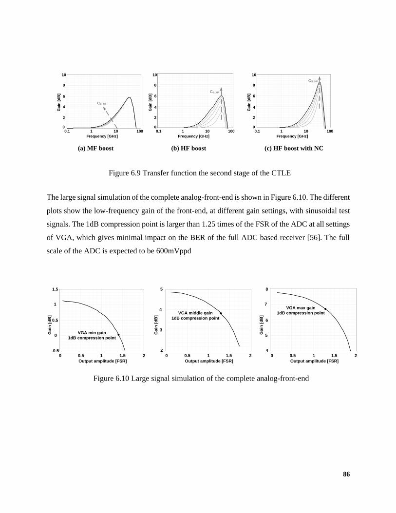
86
The large signal simulation of the complete analog-front-end is shown in Figure 6.10. The different
plots show the low-frequency gain of the front-end, at different gain settings, with sinusoidal test
signals. The 1dB compression point is larger than 1.25 times of the FSR of the ADC at all settings
of VGA, which gives minimal impact on the BER of the full ADC based receiver [56]. The full
scale of the ADC is expected to be 600mVppd
(a) MF boost (b) HF boost (c) HF boost with NC
Figure 6.9 Transfer function the second stage of the CTLE
0
2
4
6
8
10
1E+08 1E+09 1E+10 1E+11
Tit
le
Title
0
2
4
6
8
10
1E+08 1E+09 1E+10 1E+11
Tit
le
Title
Frequency [GHz]
0.1 1 10
2
4
6
8
100
Ga
in [
dB
]
0
10
Frequency [GHz]
0.1 1 10
2
4
6
8
100
Ga
in [
dB
]
0
10
Frequency [GHz]
0.1 1 10
2
4
6
8
100
Ga
in [
dB
]
0
10
0
2
4
6
8
10
1E+08 1E+09 1E+10 1E+11
Tit
le
Title
CS_HF
CS_HF
CS_MF
Figure 6.10 Large signal simulation of the complete analog-front-end
-0.5
0
0.5
1
1.5
0.00 0.50 1.00 1.50 2.00
Tit
le
Title
2
3
4
5
0.00 0.50 1.00 1.50 2.00
Tit
le
Title
4
5
6
7
8
0.00 0.50 1.00 1.50 2.00
Tit
le
Title2
1
0
Output amplitude [FSR]
0 0.5 1-0.5
0.5
1.5
Ga
in [
dB
]
1.5
2
5
3
Output amplitude [FSR]
0 0.5 1
2
4
1.5
Ga
in [
dB
]
2
8
5
Output amplitude [FSR]
0 0.5 1
4
6
1.5
Ga
in [
dB
]
7
VGA min gain
1dB compression point
VGA middle gain
1dB compression point
VGA max gain
1dB compression point
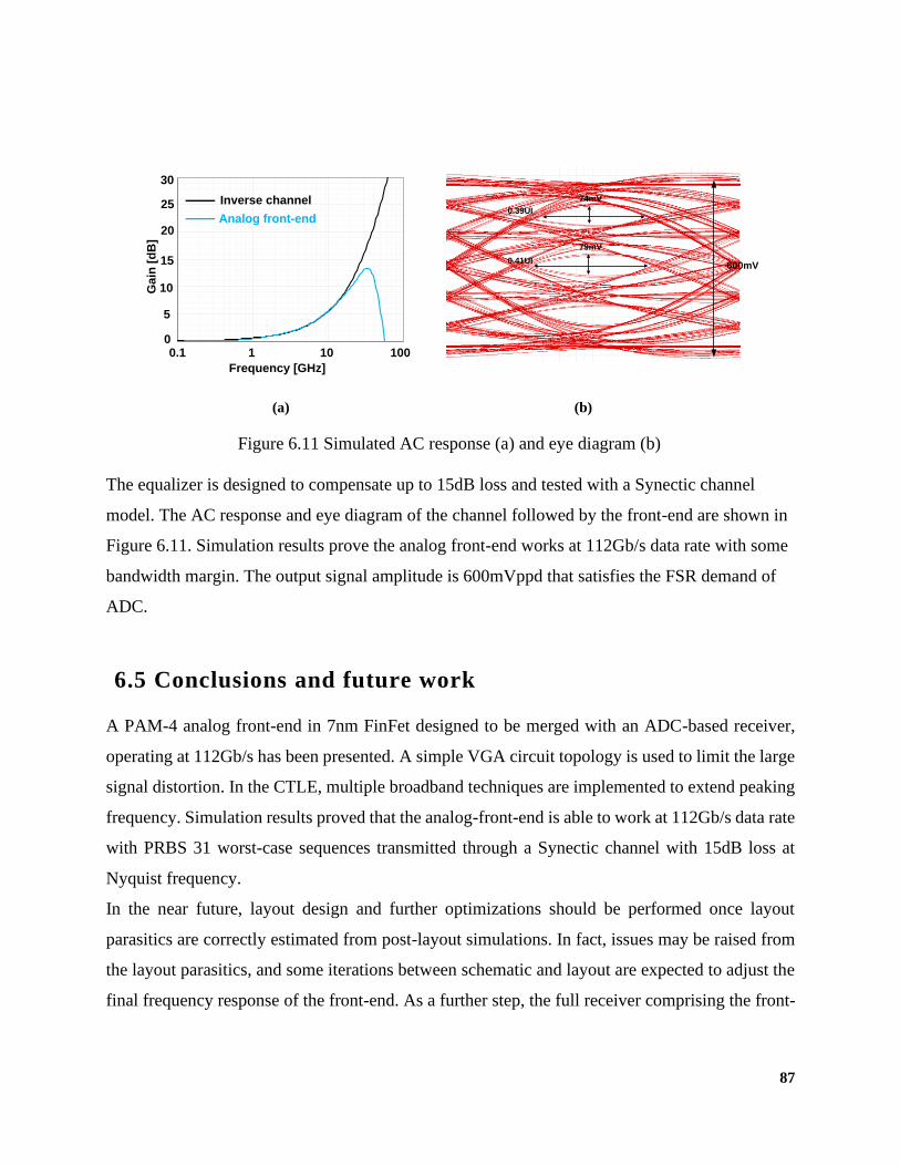
87
The equalizer is designed to compensate up to 15dB loss and tested with a Synectic channel
model. The AC response and eye diagram of the channel followed by the front-end are shown in
Figure 6.11. Simulation results prove the analog front-end works at 112Gb/s data rate with some
bandwidth margin. The output signal amplitude is 600mVppd that satisfies the FSR demand of
ADC.
6.5 Conclusions and future work
A PAM-4 analog front-end in 7nm FinFet designed to be merged with an ADC-based receiver,
operating at 112Gb/s has been presented. A simple VGA circuit topology is used to limit the large
signal distortion. In the CTLE, multiple broadband techniques are implemented to extend peaking
frequency. Simulation results proved that the analog-front-end is able to work at 112Gb/s data rate
with PRBS 31 worst-case sequences transmitted through a Synectic channel with 15dB loss at
Nyquist frequency.
In the near future, layout design and further optimizations should be performed once layout
parasitics are correctly estimated from post-layout simulations. In fact, issues may be raised from
the layout parasitics, and some iterations between schematic and layout are expected to adjust the
final frequency response of the front-end. As a further step, the full receiver comprising the front-
(a) (b)
Figure 6.11 Simulated AC response (a) and eye diagram (b)
0
5
10
15
20
25
30
1E+08 1E+09 1E+10 1E+11
Tit
le
Title
Frequency [GHz]
0.1 1 100
5
10
15
20
25
30
100
Ga
in [
dB
]
Inverse channel
Analog front-end
0.41UI
79mV
0.39UI
74mV
600mV

88
end connected to a behavioral model of the ADC has to be simulated to verify the overall
performance.
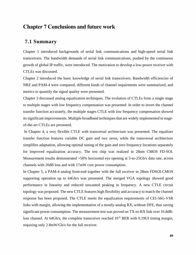
89
Chapter 7 Conclusions and future work
7.1 Summary
Chapter 1 introduced backgrounds of serial link communications and high-speed serial link
transceivers. The bandwidth demands of serial link communications, pushed by the continuous
growth of global IP traffic, were introduced. The motivation to develop a low-power receiver with
CTLEs was discussed.
Chapter 2 introduced the basic knowledge of serial link transceivers. Bandwidth efficiencies of
NRZ and PAM-4 were compared, different kinds of channel impairments were summarized, and
metrics to quantify the signal quality were presented.
Chapter 3 discussed analog equalization techniques. The evolution of CTLEs from a single stage
to multiple stages with low frequency compensation was presented. In order to invert the channel
transfer function accurately, the multiple stages CTLE with low frequency compensation showed
its significant improvements. Multiple broadband techniques that are widely implemented in stage-
of-the-art CTLEs are presented.
In Chapter 4, a very flexible CTLE with transversal architecture was presented. The equalizer
transfer function features variable DC gain and two zeros, while the transversal architecture
simplifies adaptation, allowing optimal tuning of the gain and zero frequency locations separately
for improved equalization accuracy. The test chip was realized in 28nm CMOS FD-SOI.
Measurement results demonstrated >50% horizontal eye opening at 5-to-25Gb/s data rate, across
channels with 20dB loss and with 17mW core power consumption.
In Chapter 5, a PAM-4 analog front-end together with the full receiver in 28nm FDSOI-CMOS
supporting operation up to 64Gb/s was presented. The merged VGA topology showed good
performance in linearity and reduced unwanted peaking in frequency. A new CTLE circuit
topology was proposed. The new CTLE features high flexibility and accuracy to match the channel
response has been proposed. The CTLE meets the equalization requirements of CEI-56G-VSR
links with margin, allowing the implementation of a mostly-analog RX, without DFE, thus saving
significant power consumption. The measurement test was proved on TX-to-RX link over 16.8dB-
loss channel. At 64Gb/s, the complete transceiver reached 10-6 BER with 0.19UI timing margin,
requiring only 2.8mW/Gb/s for the full receiver.
90
In Chapter 6, a PAM-4 analog front-end in 7nm FinFet for an ADC based receiver operating up to
112Gb/s was presented. A simple VGA circuit topology was used in architecture to limit the large
signal distortion. Multiple broadband techniques were also implemented to extend peaking
frequency. Simulation results proved that the analog-front-end was able to work at 112Gb/s data
rate with PRBS 31 worst-case sequences transmitted through a Synectic channel with 15dB loss
at Nyquist frequency.
7.2 Future work
The demand for a higher speed serial link is unstoppable. The fast-growing cloud services are
pushing the development of higher speed data centers [14]. The >100Gb/s serial links per lane for
the next generation 800Gb Ethernet are currently exploited. For the 112Gb/s PAM-4 analog front-
end in 7nm FinFet, optimizing the performance after post-layout extraction is the nearest target.
Since there are many layout dependent effects that impact the bandwidth and linearity, some
iterations between schematic and layout are expected to adjust the final response of the front-end.
The physical layers of serial link transceivers are moving to advanced FinFet technology nodes.
The transceivers with ADC-based receivers have shown its powerful performance [57] in long-
reach channels (>30dB loss). However, the ADC is still a power-hungry component. For short -
reach link (<20dB loss), a full-analog solution is also attractive to save power. In 16nm/7nm FinFet
technology, analog designs are constrained by scaled supply voltage, parasitics of Fins and layout
dependent effects. In order to realize a compact full-analog receiver, some new circuit topologies
should be exploited. For example, replacing long-channel length transistors with stack of short-
channel length transistors to make current tails saves area and reduces the parasitic resistance [55].
The very flexible CTLE with transverse architecture presented in Chapter 3was not applied to
56Gb/s or 112Gb/s PAM-4 receivers. The reason is that the linearity of high-resolution VGAs
impacts the PAM-4 system more than the NRZ system. To incorporate this CTLE architecture, it
is rewarding to exploit new techniques to keep high linearity of VGAs.
91
References:
[1] Cisco Global Cloud Index: Forecast and Methodology, 2014–2019 White paper, 2016.
[Online]. Available:
https://www.cisco.com/c/dam/m/en_us/serviceprovider/ciscoknowledgenetwork/files/547_1
1_10-15-DocumentsCisco_GCI_Deck_2014-2019_for_CKN__10NOV2015_.pdf
[2] Cisco Visual Networking Index: Forecast and Trends, 2017–2022 White Paper, 2019.
[Online]. Available: https://www.cisco.com/c/en/us/solutions/collateral/service-
provider/visual-networking-index-vni/white-paper-c11-741490.html
[3] OIF's CEI 56G Interfaces –Key Building Blocks for Optics in the 400G Data Center, 2015.
[Online]. Available: https://www.oiforum.com/wp-content/uploads/2019/01/150928_Mkt-
Focus-ECOC-Panel-OIF.pdf
[4] Demystifying 40 Gigabit Ethernet Physical Layer Interfaces in Data Centers, Synopsis,
[Online]. Available: https://www.synopsys.com/designware-ip/technical-
bulletin/demystifying-40-interfaces.html
[5] J. Liu, X. Lin, “Equalization in high-speed communication systems”, IEEE Circuits and
Systems Magazine vol. 4, no. 2, 2004.
[6] B. Razavi, Design of Integrated Circuits for Optical Communications, M. G. Hill, 2nd Ed.,
2012.
[7] Y.Frans, J. Shin, L. Zhou, P. Upadhyaya, J. Im, V. Kireev, M. Elzeftawi, H. Hedayati, T.
Pham, S. Asuncion, C. Borrelli, G. Zhang, H. Zhang, and K. Chang, “A 56-Gb/s PAM4
Wireline Transceiver Using a 32-Way Time-Interleaved SAR ADC in 16-nm FinFET”,
IEEE Journal of Solid State Circuits (JSSC), vol. 52, pp. 1101 - 1110, January 2017.
[8] W. Dally, Digital Systems Engineering 1st Edition, Cambridge Univ. Press, 1st Ed., 2008
[9] IC Package, Fujitsu, 2011. [Online]. Available:
https://www.fujitsu.com/cn/en/Images/a810000114e-en.pdf
[10] Adee Ran, Kent Lusted “Accounting for transmitter noise in system budget”, 2013. [Online]. Available: http://www.ieee802.org/3/bj/public/jul13/ran_3bj_01a_0713.pdf
[11] SerDes Design Part 4: Frequency Domain Analysis for High Data Rate SerDes Links,
Mentor, 2018. [Online]. Available:
https://blogs.mentor.com/hyperblog/blog/2018/04/01/serdes-design-part-4-frequency-
domain-analysis-for-high-data-rate-serdes-links/
[12] IEEE 802.3ap, Insertion Loss to Crosstalk Ratio (ICR) [Online]. Available:
http://www.ieee802.org/3/ap/public/may06/healey_02_0506.pdf
[13] IEEE 802.3bj: 100GBASE-CR4 Specifications [Online].Available:
http://www.ieee802.org/3/bj/public/may12/diminico_01a_0512.pdf
[14] The 2018 Ethernet Roadmap, Ethernet alliance. [Online]. Available:
https://ethernetalliance.org/the-2018-ethernet-roadmap/
92
[15] T. Anand, "Wireline Link Performance Survey," [Online]. Available:
https://web.engr.oregonstate.edu/~anandt/linksurvey
[16] F. Loi, E. Mammei, F. Radice, M. Bruccoleri, S. Erba, M. Bassi, and A. Mazzanti, “A 25-
Gb/s FIR equalizer based on highly linear all-pass delay line stages in 28-nm LP CMOS," in
IEEE Radio Frequency Integrated Circuits Symposium (RFIC), May 2015.
[17] E. Depaoli ; E. Monaco ; G. Steffan ; M. Mazzini ; H. Zhang ; W. Audoglio ; O. Belotti ; A.
A. Rossi ; G. Albasini ; M. Pozzoni ; S. Erba ; A. Mazzanti, “A 4.9pJ/b 16-to-64Gb/s PAM-
4 VSR transceiver in 28nm FDSOI CMOS” in IEEE International Solid - State Circuits
Conference - (ISSCC), February, 2018.
[18] W.-Z. Chen, S.-H. Huang, G.-W. Wu, C.-C. Liu, Y.-T. Huang, C.-F. Chiu, W.-H. Chang,
Y.-Z. Juang, A 3.125 Gbps CMOS fully integrated optical receiver with adaptive analog
equalizer, in IEEE Asian Solid-State Circuits Conference 2007 (ASSCC’07), November,
2007.
[19] S. Parikh T. Kao, Y. Hidaka, J. Jiang, A. Toda, S. Mcleod, W. Walker, Y. Koyanagi, T.
Shibuya, J. Yamada, “A 32Gb/s Wireline Receiver with a Low-Frequency Equalizer,
CTLE and 2-Tap DFE in 28nm CMOS”, in IEEE International Solid - State Circuits
Conference - (ISSCC), February 2013.
[20] B. Zhang, K. Khanoyan, H. Hatamkhani, H. Tong, K. Hu, S. Fallahi, K. Vakilian, A.
Brewster, “A 28Gb/s Multi-Standard Serial-Link Transceiver for Backplane Applications in
28nm CMOS”, in IEEE International Solid - State Circuits Conference - (ISSCC), February
2015.
[21] C. Gasca, S. Pueyo, C. Chagoyen, CMOS Continuous- Time Adaptive Equalizers for High-
Speed Serial Links, Springer, 2015.
[22] S. Shahramian, C. Ting, A. Sheikholeslami, H. Tamura, M. Kibune, “A Pattern-Guided
Adaptive Equalizer in 65nm CMOS”, in IEEE International Solid - State Circuits
Conference - (ISSCC), February 2011.
[23] P. Francese, M. Brändli, C. Menolfi, M. Kossel, T. Morf, L. Kull, A. Cevrero, H.Yueksel, I.
Oezkaya, D. Luu, T. Toifl, “A 30Gb/s 0.8pJ/b 14nm FinFET receiver data-path”, in IEEE
International Solid-State Circuits Conference (ISSCC), February, 2016.
[24] Y.M. Ying and S.I. Liu, “A 20Gb/s digitally adaptive equalizer/DFE with blind sampling”,
in IEEE International Solid-State Circuits Conference (ISSCC), February, 2011.
[25] J. Lee, “A 20-Gb/s adaptive equalizer in 0.13-μm CMOS technology”, IEEE Journal of
Solid-State Circuits, vol. 41, no. 9, pp. 2058–2066, September 2006.
[26] H.Y. Joo, K.-S. Ha, and L.-S. Kim, “Data Pattern-Tolerant Adaptive Equalizer Using
Spectrum Balancing Method”, Proceedings IEEE Symposium on VLSI circuits, 2009.
[27] W. S. Kim, C. K. Seong, and W. Y. Choi, “A 5.4Gb/s adaptive equalizer using
asynchronous-sampling histograms”, in IEEE International Solid-State Circuits Conference
(ISSCC), February 2011.
[28] Y.-F. Lin, et al., “A 5-20 Gb/s Power Scalable Adaptive Linear Equalizer Using Edge
Counting”, in Proceedings IEEE Asian Solid-State Circuits Conf. (ASSCC), November,
2014.
93
[29] H. Zhang, E. Monaco, M. Bassi, A. Mazzanti, “Five to 25 Gb/s continuous time linear
equaliser with transversal architecture”, IET Electronics Letters, vol.53, no.10, Dec. 2017,
pp.1629-1630.
[30] A. Carusone and D. A. Johns, "Analogue adaptive filters: past and present", in IEEE
Proceedings Circuits, Devices and Systems, vol. 147, no. 1, pp. 82-90, Feb 2000.”
[31] J. E. Proesel and T. O. Dickson, “A 20-Gb/s, 0.66-pJ/bit serial receiver with 2-stage
continuous-time linear equalizer and 1-tap deci-sion feedback equalizer in 45 nm SOI
CMOS”, in Proceedings IEEE Symposium on VLSI circuits 2011.
[32] K. Jung, A. Amirkhany, K. Kaviani, “A 0.94mW/Gb/s 22Gb/s 2-tap partial-response DFE
receiver in 40nm LP CMOS”, in IEEE International Solid-State Circuits Conference
(ISSCC), February 2013.
[33] OIF's CEI 56G Interfaces – Key Building Blocks for Optics in the 400G Data Center,
[Online]. Available: https://www.oiforum.com/wp-content/uploads/2019/01/150928_Mkt-
Focus-ECOC-Panel-OIF.pdf/
[34] K. Gopalakrishnan et al., "3.4 A 40/50/100Gb/s PAM-4 Ethernet transceiver in 28nm
CMOS," in IEEE International Solid-State Circuits Conference (ISSCC), February, 2016
[35] J. Im et al., "A 40-to-56 Gb/s PAM-4 Receiver With Ten-Tap Direct Decision-Feedback
Equalization in 16-nm FinFET," in IEEE Journal of Solid-State Circuits, vol. 52, no. 12, pp.
3486-3502, Dec. 2017.
[36] L. Wang, Y. Fu, M. LaCroix, E. Chong and A. C. Carusone, "A 64Gb/s PAM-4 transceiver
utilizing an adaptive threshold ADC in 16nm FinFET," in IEEE International Solid-State
Circuits Conference (ISSCC), February, 2018.
[37] P. Upadhyaya et al., "A fully adaptive 19-to-56Gb/s PAM-4 wireline transceiver with a
configurable ADC in 16nm FinFET," I in IEEE International Solid-State Circuits
Conference (ISSCC), February, 2018.
[38] J. Kim et al., "A 112Gb/s PAM-4 transmitter with 3-Tap FFE in 10nm CMOS," in IEEE
International Solid-State Circuits Conference (ISSCC), February 2018.
[39] C. Menolfi et al., "A 112Gb/S 2.6pJ/b 8-Tap FFE PAM-4 SST TX in 14nm CMOS," in
IEEE International Solid-State Circuits Conference (ISSCC), February 2018.
[40] J. L. Zerbe et al., "Equalization and clock recovery for a 2.5-10-Gb/s 2-PAM/4-PAM
backplane transceiver cell," in IEEE Journal of Solid-State Circuits, vol. 38, no. 12, pp.
2121-2130, Dec. 2003.
[41] J. Kim, et al., "A 16-to-40Gb/s quarter-rate NRZ/PAM4 dual-mode transmitter in 14nm
CMOS," in IEEE International Solid-State Circuits Conference (ISSCC), February 2015.
[42] M. Bassi, F. Radice, M. Bruccoleri, S. Erba and A. Mazzanti, "A 45Gb/s PAM-4 transmitter
delivering 1.3Vppd output swing with 1V supply in 28nm CMOS FDSOI," in IEEE
International Solid-State Circuits Conference (ISSCC), February 2016.
[43] T. O. Dickson et al.: "A 1.8pJ/b 56Gb/s PAM-4 Transmitter with Fractionally Spaced FFE in
14nm CMOS”, IEEE International Solid-State Circuits Conference (ISSCC), February 2017.

94
[44] G.Steffan et al.: “A 64Gb/s PAM-4 Transmitter with 4-Tap FFE and 2.26pJ/b Energy
Efficiency in 28nm CMOS FDSOI,” in IEEE International Solid-State Circuits Conference
(ISSCC), February 2017.
[45] A. Roshan-Zamir, O. Elhadidy, H. W. Yang and S. Palermo, "A Reconfigurable 16/32 Gb/s
Dual-Mode NRZ/PAM4 SerDes in 65-nm CMOS," in IEEE Journal of Solid-State Circuits,
vol. 52, no. 9, pp. 2430-2447, Sept. 2017.
[46] S. Palermo et al., "CMOS ADC-based receivers for high-speed electrical and optical links,"
in IEEE Communications Magazine, vol. 54, no. 10, pp. 168-175, October 2016.
[47] D. Cui et al., "3.2 A 320mW 32Gb/s 8b ADC-based PAM-4 analog front-end with
programmable gain control and analog peaking in 28nm CMOS," in IEEE International
Solid-State Circuits Conference (ISSCC), February 2016.
[48] Aurangozeb, A. D. Hossain, M. Mohammad and M. Hossain, "Channel-Adaptive ADC and
TDC for 28 Gb/s PAM-4 Digital Receiver," in IEEE Journal of Solid-State Circuits, vol. 53,
no. 3, pp. 772-788, March 2018.
[49] P.-J.Peng et al., “A 56Gb/s PAM-4/NRZ Transceiver in 40nm CMOS”, in IEEE
International Solid-State Circuits Conference (ISSCC), February 2017.
[50] E. Mammei et al., "Analysis and Design of a Power-Scalable Continuous-Time FIR
Equalizer for 10 Gb/s to 25 Gb/s Multi-Mode Fiber EDC in 28 nm LP CMOS," in IEEE
Journal of Solid-State Circuits, vol. 49, no. 12, pp. 3130-3140, Dec. 2014.
[51] Chih-Fan Liao and Shen-Iuan Liu, "A 10Gb/s CMOS AGC Amplifier with 35dB Dynamic
Range for 10Gb Ethernet," in IEEE International Solid-State Circuits Conference (ISSCC),
February 2006.
[52] IEEE 802.3, 52Gb/s Chip to Module Channels using zQSFP+, [Online]. Available:
http://www.ieee802.org/3/bs/public/14_11/dudek_3bs_01_1114.pdf
[53] IEEE 802.3ck, [Online]. Available: http://www.ieee802.org/3/ck/
[54] 7nm Technology, [Online]. Available:
https://www.tsmc.com/english/dedicatedFoundry/technology/7nm.htm
[55] Alvin L. S. Loke, et. “Analog/mixed-signal design challenges in 7-nm CMOS and beyond”,
in IEEE Custom Integrated Circuits Conference (CICC), 2018.
[56] Sam Palermo, et. “Analog-to-Digital Converter-Based Serial Links: An overview”, in IEEE
Solid-State Circuits Magazine, 2018.
[57] Matteo Pisati, et. “A Sub-250mW 1-to-56Gb/s Continuous-Range PAM-4 42.5dB IL
ADC/DAC-Based Transceiver in 7nm FinFET”, in IEEE International Solid-State Circuits
Conference (ISSCC), February 2019.
[58] The 2016 Ethernet Roadmap, Ethernet alliance. [Online]. Available:
https://ethernetalliance.org/roadmap/
[59] Intel, AN 835: PAM4 Signaling Fundamentals, [Online]. Available:
https://www.intel.com/content/www/us/en/programmable/documentation/qjz151251236455
0.html#yqa1512517379332
95
[60] A Design of Experiments for Gigabit Serial Backplane Channels, Keysight, [Online].
Available: http://literature.cdn.keysight.com/litweb/pdf/5989-8864EN.pdf
[61] F. Loi, “Adaptive Analog Transversal Equalizers for High-Speed Serial Links”, Ph.D.
dissertation, University of Pavia, 2015.
[62] V. Stojanovic, “Channel-limited high-speed links: Modeling, analysis and design,” Ph.D.
dissertation, Stanford University, 2004.
[63] H. Uchiki, Y. Ota, M. Tani, Y. Hayakawa, K. Asahina, “A 6Gb/s RX Equalizer Adapted Using
Direct Measurement of the Equalizer Output Amplitude” in IEEE International Solid-State
Circuits Conference (ISSCC), February 2008.
[64] F. Gerfers, G. Besten, P. Petkov, J. Conder, A. Koellmann, “A 0.2–2 Gb/s 6x OSR Receiver
Using a Digitally Self-Adaptive Equalizer”, in IEEE Journal of Solid-State Circuits, vol. 43,
no. 6, pp. 1436 - 1448, June 2008.
96
Appendix
List of publications:
[1] H. Zhang ; E. Monaco ; M. Bassi ; A. Mazzanti “Five to 25Gb/s continuous time linear
equaliser with transversal architecture” in Electronics Letters, Volume: 53, Issue: 25, Pages: 1629
– 1630, 2017.
[2] H. Zhang ; E. Monaco ; M. Bassi ; A. Mazzanti , “Flexible Transversal Continuous-Time
Linear Equalizer Operating up to 25Gb/s in 28nm CMOS” in IEEE International Symposium on
Circuits and Systems (ISCAS), May 2018.
[3] Emanuele Depaoli ; Enrico Monaco ; Giovanni Steffan ; Marco Mazzini ; Hongyang Zhang ;
Walter Audoglio ; Oscar Belotti ; Augusto Andrea Rossi ; Guido Albasini ; Massimo Pozzoni ;
Simone Erba ; Andrea Mazzanti, “A 4.9pJ/b 16-to-64Gb/s PAM-4 VSR transceiver in 28nm
FDSOI CMOS” in IEEE International Solid - State Circuits Conference (ISSCC), Feburary 2018.
[4] E. Depaoli, H. Zhang, M. Mazzini, W. Audoglio, A. A. Rossi, G. Albasini, M. Pozzoni, S.
Erba, E. Temporiti, A. Mazzanti, “A 64Gb/s Low-Power Transceiver for Short- Reach PAM-4
Electrical Links in 28nm FDSOI CMOS” in Journal of Solid-State Circuits (JSSC) Volume: 54 ,
Issue: 1, January 2019.


![Alessandro Reali Curriculum Vitˆ - unipv · Alessandro Reali Curriculum Vitˆ [Last update: December 7th, 2018] 1 Contacts - Born in Pavia (PV) on February 28th, 1977 - Marital status:](https://static.fdocuments.in/doc/165x107/5c69746209d3f25c6a8d19d4/alessandro-reali-curriculum-vit-unipv-alessandro-reali-curriculum-vit.jpg)


![RICERCA @UNIPVnews.unipv.it/wp-content/uploads/2017/01/bozza-31-maggio-pagine-A4_light.pdf · Cortile delle Magnolie, Università di Pavia RICERCA @UNIPV lniie^f^gmhZeeZm^lmZmZngbio'g^plbeFZ`Zsbg^]^eeNgbo^klbm¨]bIZobZ](https://static.fdocuments.in/doc/165x107/5e211b904ff4a2195948e4f0/ricerca-cortile-delle-magnolie-universit-di-pavia-ricerca-unipv-lniiefgmhzeezmlmzmzngbiogplbefzzsbgeengboklbmbizobz.jpg)