System in Package Solutions using Fan-Out Wafer Level Packaging Technology
31
System in Package Solutions using Fan-Out Wafer Level Packaging Technology J. Campos; S. Kroehnert; E. O’Toole; V. Henriques; V. Chatinho; A. Martins; J. Teixeira; A. Cardoso; A. Janeiro; I. Barros; O. Tavares; R. Almeida June 27 th , 2013 SEMI Networking Day: Packaging - Key for System Integration
Transcript of System in Package Solutions using Fan-Out Wafer Level Packaging Technology
System in Package Solutions using
Fan-Out Wafer Level Packaging Technology
J. Campos; S. Kroehnert; E. O’Toole; V. Henriques; V. Chatinho; A. Martins;
J. Teixeira; A. Cardoso; A. Janeiro; I. Barros; O. Tavares; R. Almeida
June 27th, 2013
SEMI Networking Day:
Packaging - Key for System Integration
Nanium · SiP Solutions using FO-WLP, June 27th, 2013; Internal Use
Content
Introduction to FO-WLP and WLSiP
Enablers of WLSiP
WLSiP developments based on FO-WLP
Summary & Conclusions
Acknowledgement
2

Nanium · SiP Solutions using FO-WLP, June 27th, 2013; Internal Use
Content
Introduction to FO-WLP and WLSiP
Enablers of WLSiP
WLSiP developments based on FO-WLP
Summary & Conclusions
Acknowledgement
3
Nanium · SiP Solutions using FO-WLP, June 27th, 2013; Internal Use
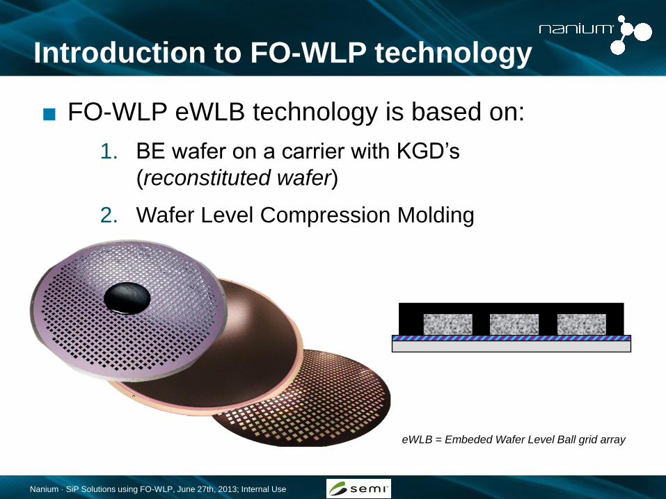
Introduction to FO-WLP technology
■ FO-WLP eWLB technology is based on:
1. BE wafer on a carrier with KGD’s
(reconstituted wafer)
2. Wafer Level Compression Molding
4
eWLB = Embeded Wafer Level Ball grid array
Nanium · SiP Solutions using FO-WLP, June 27th, 2013; Internal Use
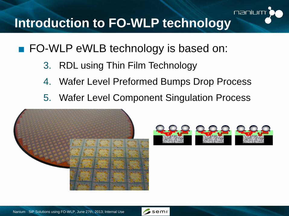
■ FO-WLP eWLB technology is based on:
3. RDL using Thin Film Technology
4. Wafer Level Preformed Bumps Drop Process
5. Wafer Level Component Singulation Process
Introduction to FO-WLP technology
5
Nanium · SiP Solutions using FO-WLP, June 27th, 2013; Internal Use
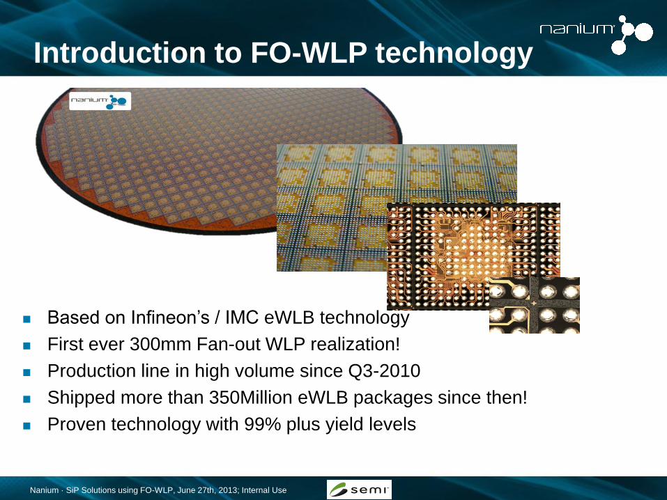
Based on Infineon’s / IMC eWLB technology
First ever 300mm Fan-out WLP realization!
Production line in high volume since Q3-2010
Shipped more than 350Million eWLB packages since then!
Proven technology with 99% plus yield levels
Introduction to FO-WLP technology
6

Nanium · SiP Solutions using FO-WLP, June 27th, 2013; Internal Use
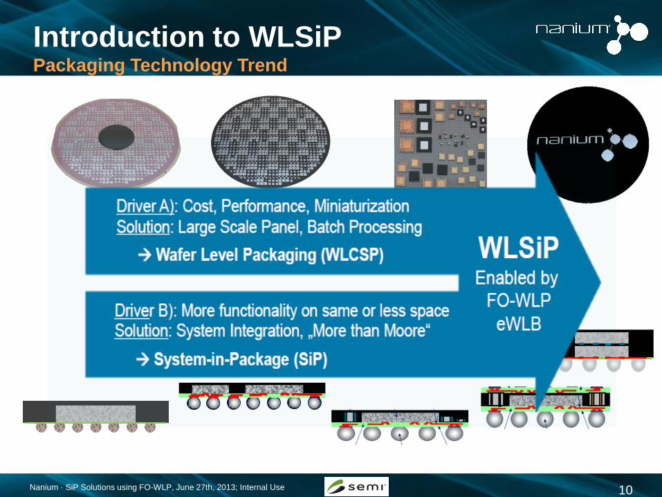
Advantages of FO-WLP technology
Diameter of the reconstituted wafer independent of original
silicon wafer;
Adaptable fan-out area and solution for I/O Gap;
Smaller and Thinner form factor;
Improved electrical and thermal performance;
Lower unit cost due to 300mm wafer level batch
processing;
Simplification of Bill of Material, Supply Chain and
Manufacturing Infrastructure;
Enabler for SiP / 3D Integration and further miniaturization
WLSiP System-in-Package on Wafer Level
7
Nanium · SiP Solutions using FO-WLP, June 27th, 2013; Internal Use
Introduction to WLSiP Packaging Technology Trend
8
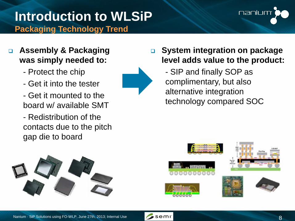
Assembly & Packaging
was simply needed to:
- Protect the chip
- Get it into the tester
- Get it mounted to the
board w/ available SMT
- Redistribution of the
contacts due to the pitch
gap die to board
System integration on package
level adds value to the product:
- SIP and finally SOP as
complimentary, but also
alternative integration
technology compared SOC
Nanium · SiP Solutions using FO-WLP, June 27th, 2013; Internal Use
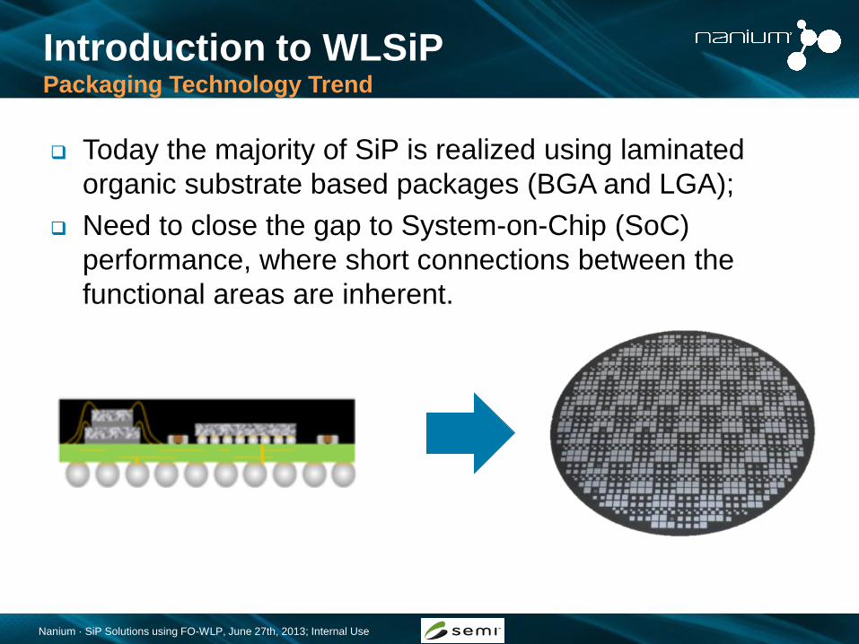
Today the majority of SiP is realized using laminated
organic substrate based packages (BGA and LGA);
Need to close the gap to System-on-Chip (SoC)
performance, where short connections between the
functional areas are inherent.
Introduction to WLSiP Packaging Technology Trend
Nanium · SiP Solutions using FO-WLP, June 27th, 2013; Internal Use 10
Introduction to WLSiP Packaging Technology Trend
Nanium · SiP Solutions using FO-WLP, June 27th, 2013; Internal Use
Content
Introduction to FO-WLP and WLSiP
Enablers of WLSiP
WLSiP developments based on FO-WLP
Summary & Conclusions
Acknowledgement
11
Nanium · SiP Solutions using FO-WLP, June 27th, 2013; Internal Use 12
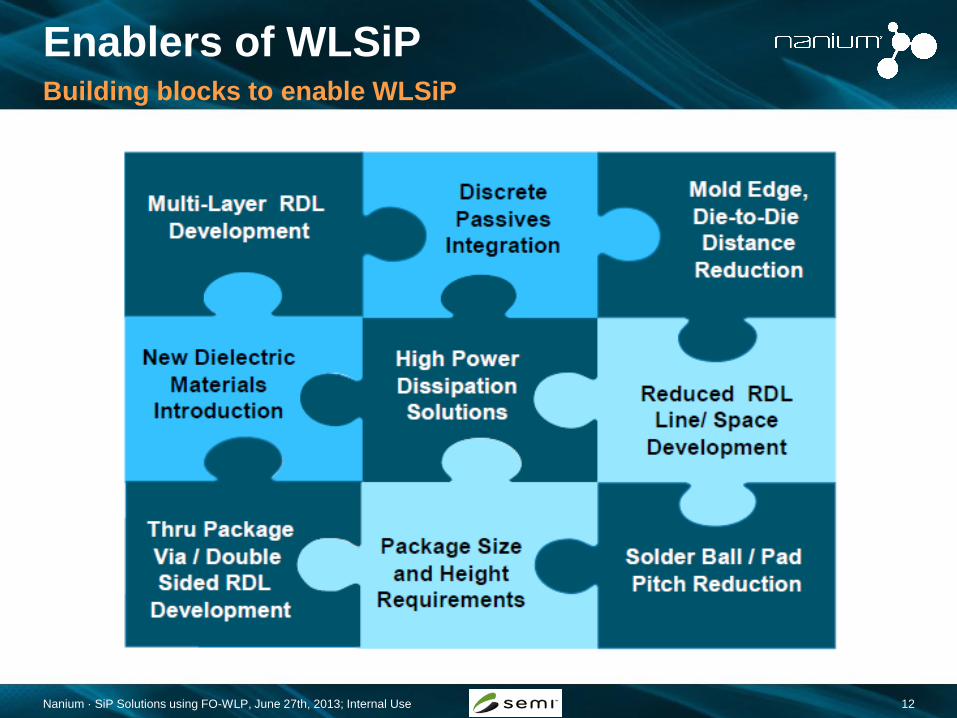
Enablers of WLSiP Building blocks to enable WLSiP
Nanium · SiP Solutions using FO-WLP, June 27th, 2013; Internal Use 13
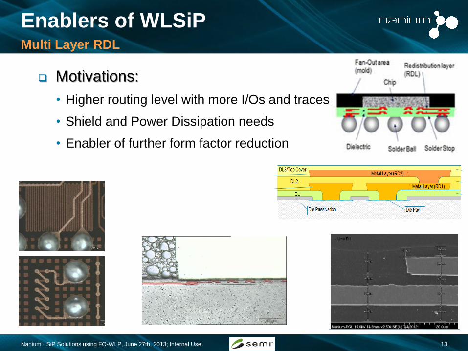
Enablers of WLSiP Multi Layer RDL
Motivations:
• Higher routing level with more I/Os and traces
• Shield and Power Dissipation needs
• Enabler of further form factor reduction
Nanium · SiP Solutions using FO-WLP, June 27th, 2013; Internal Use 14
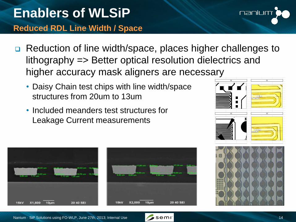
Enablers of WLSiP Reduced RDL Line Width / Space
Reduction of line width/space, places higher challenges to
lithography => Better optical resolution dielectrics and
higher accuracy mask aligners are necessary
• Daisy Chain test chips with line width/space
structures from 20um to 13um
• Included meanders test structures for
Leakage Current measurements
S1 S1
S2 S2
Nanium · SiP Solutions using FO-WLP, June 27th, 2013; Internal Use 15
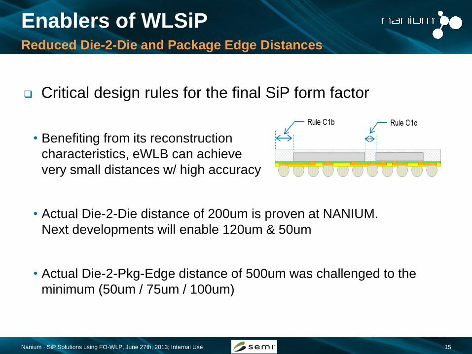
Enablers of WLSiP Reduced Die-2-Die and Package Edge Distances
Critical design rules for the final SiP form factor
• Benefiting from its reconstruction
characteristics, eWLB can achieve
very small distances w/ high accuracy
• Actual Die-2-Die distance of 200um is proven at NANIUM.
Next developments will enable 120um & 50um
• Actual Die-2-Pkg-Edge distance of 500um was challenged to the
minimum (50um / 75um / 100um)
Nanium · SiP Solutions using FO-WLP, June 27th, 2013; Internal Use 16
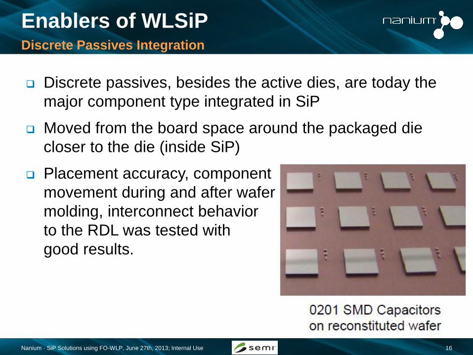
Enablers of WLSiP Discrete Passives Integration
Discrete passives, besides the active dies, are today the
major component type integrated in SiP
Moved from the board space around the packaged die
closer to the die (inside SiP)
Placement accuracy, component
movement during and after wafer
molding, interconnect behavior
to the RDL was tested with
good results.

Nanium · SiP Solutions using FO-WLP, June 27th, 2013; Internal Use
Content
Introduction to FO-WLP and WLSiP
Enablers of WLSiP
WLSiP developments based on FO-WLP
Summary & Conclusions
Acknowledgement
17
Nanium · SiP Solutions using FO-WLP, June 27th, 2013; Internal Use
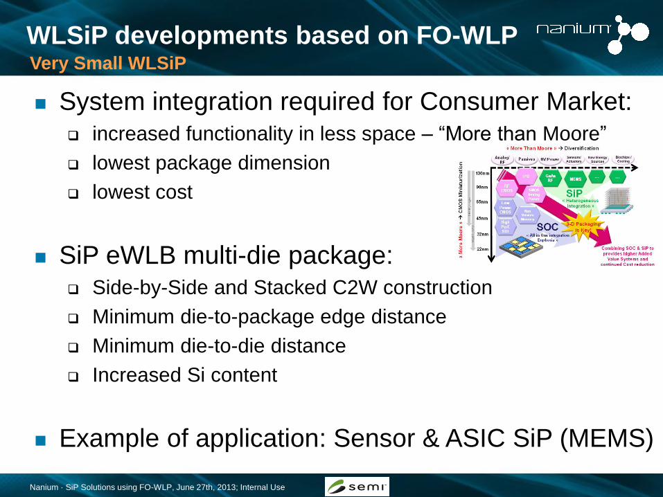
System integration required for Consumer Market:
increased functionality in less space – “More than Moore”
lowest package dimension
lowest cost
SiP eWLB multi-die package:
Side-by-Side and Stacked C2W construction
Minimum die-to-package edge distance
Minimum die-to-die distance
Increased Si content
Example of application: Sensor & ASIC SiP (MEMS)
WLSiP developments based on FO-WLP Very Small WLSiP
Nanium · SiP Solutions using FO-WLP, June 27th, 2013; Internal Use
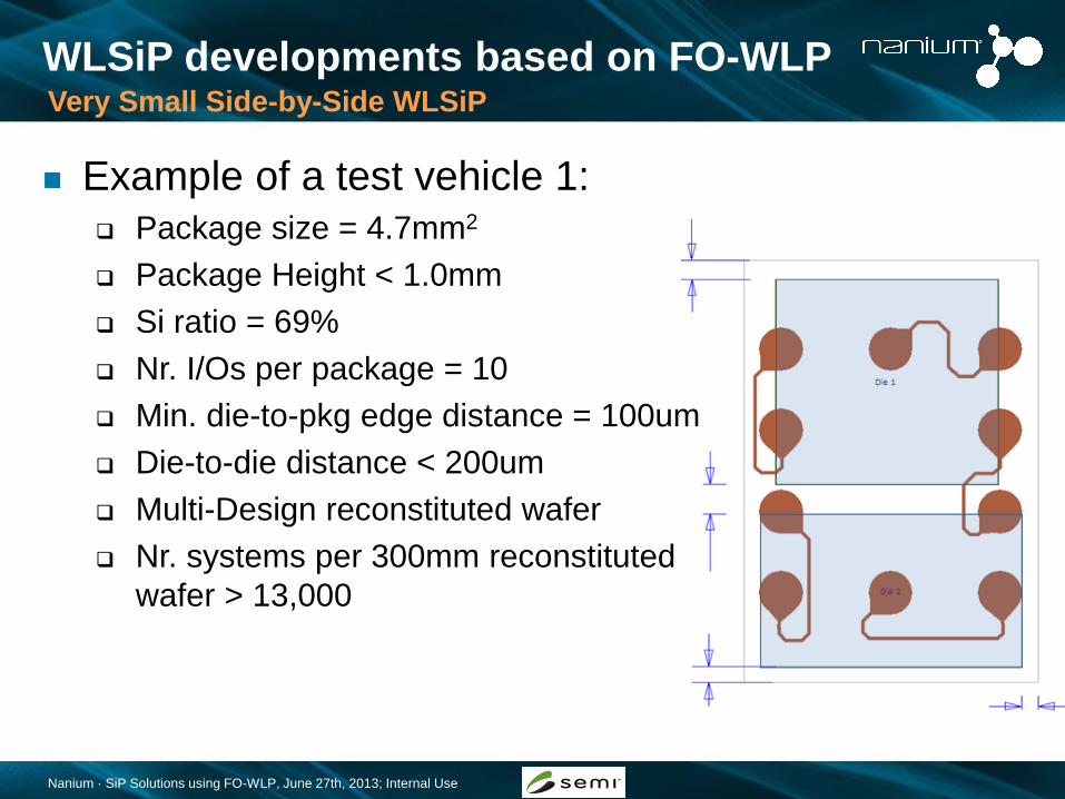
Example of a test vehicle 1:
Package size = 4.7mm2
Package Height < 1.0mm
Si ratio = 69%
Nr. I/Os per package = 10
Min. die-to-pkg edge distance = 100um
Die-to-die distance < 200um
Multi-Design reconstituted wafer
Nr. systems per 300mm reconstituted
wafer > 13,000
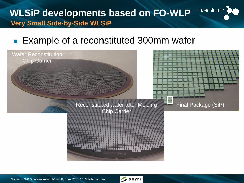
WLSiP developments based on FO-WLP Very Small Side-by-Side WLSiP
Nanium · SiP Solutions using FO-WLP, June 27th, 2013; Internal Use
Example of a reconstituted 300mm wafer
Wafer Reconstitution
Chip Carrier
Final Package (SiP) Reconstituted wafer after Molding
Chip Carrier
WLSiP developments based on FO-WLP Very Small Side-by-Side WLSiP
Nanium · SiP Solutions using FO-WLP, June 27th, 2013; Internal Use
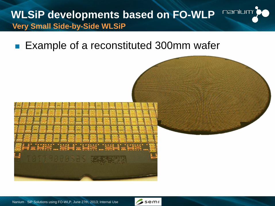
Example of a reconstituted 300mm wafer
WLSiP developments based on FO-WLP Very Small Side-by-Side WLSiP
Nanium · SiP Solutions using FO-WLP, June 27th, 2013; Internal Use
High Density integration for custom applications:
Enhanced electrical & thermal performance
Substrate less technology
Smaller form factor & reduced module thickness
SiP eWLB with side-by-side multi-die package:
Increased number of active devices (e.g:10)
Minimum die-to-die distance
RDL & u-bumping & Edge Connectors as a replacement of
interposers and other interconnect elements
WLSiP developments based on FO-WLP Highly Integrated Side-by-Side WLSiP
Nanium · SiP Solutions using FO-WLP, June 27th, 2013; Internal Use
Heterogeneous integration for flexible product
design:
Easy integration of active & passive devices
Flexible integration of devices of different types and with
different form factors
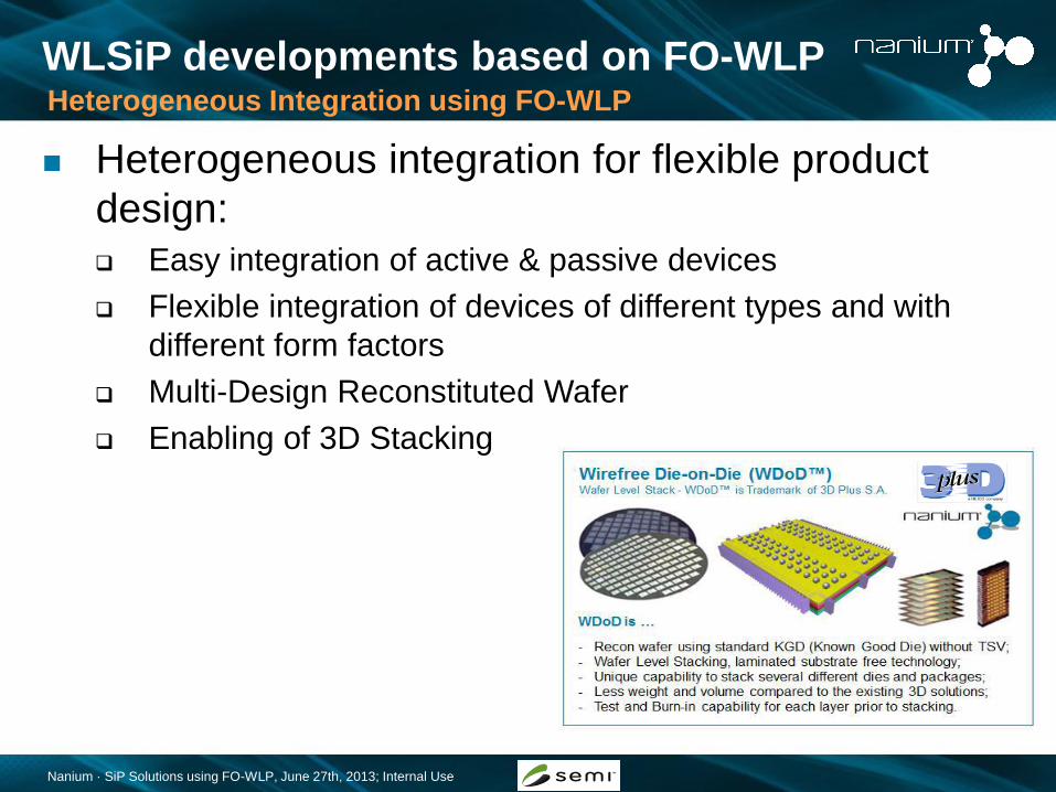
Multi-Design Reconstituted Wafer
Enabling of 3D Stacking
WLSiP developments based on FO-WLP Heterogeneous Integration using FO-WLP
Nanium · SiP Solutions using FO-WLP, June 27th, 2013; Internal Use
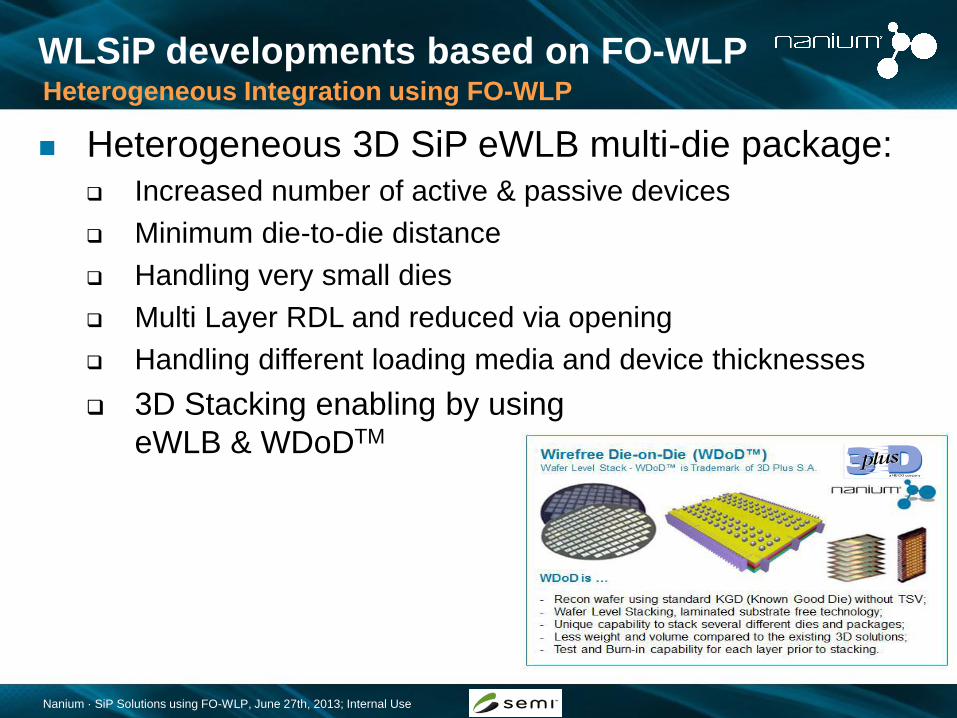
Heterogeneous 3D SiP eWLB multi-die package:
Increased number of active & passive devices
Minimum die-to-die distance
Handling very small dies
Multi Layer RDL and reduced via opening
Handling different loading media and device thicknesses
3D Stacking enabling by using
eWLB & WDoDTM
WLSiP developments based on FO-WLP Heterogeneous Integration using FO-WLP

Nanium · SiP Solutions using FO-WLP, June 27th, 2013; Internal Use
WLSiP developments based on FO-WLP Heterogeneous Integration using FO-WLP
Example of a test module 1:
Module size ~ 38mm2
Module Height = 0.2mm
Nr. dies per module = 2 active + 7 Cap
+ 1 Diode
Die-to-die distance < 200um
Min. Die size = 660um

Nanium · SiP Solutions using FO-WLP, June 27th, 2013; Internal Use
Example of a test module 2:
Module size = 361mm2
Module Height = 0.2mm
Nr. dies per module = 3
Die pad size & pitch = 47um / 52um
staggered
Multi Layer RDL
Via opening = 15um
Line Width / space = 20um
WLSiP developments based on FO-WLP Heterogeneous Integration using FO-WLP
Nanium · SiP Solutions using FO-WLP, June 27th, 2013; Internal Use
Content
Introduction to FO-WLP and WLSiP
Enablers of WLSiP
WLSiP developments based on FO-WLP
Summary & Conclusions
Acknowledgement
27
Nanium · SiP Solutions using FO-WLP, June 27th, 2013; Internal Use
Summary & Conclusions
eWLB is a FO-WLP technology that presents competitive
advantages to enable SiP solutions based on WLP
Enabling of WLSiP requires the development of several
technology bricks like:
multi-layer RDL;
fine RDL line width & space;
reduced die-2-die & die-2-package edge distances
integration of discrete passive devices
NANIUM has sucessfully completed several development
projects on its FO-WLP eWLB technology in the direction
of WLSiP
28
Nanium · SiP Solutions using FO-WLP, June 27th, 2013; Internal Use
Summary & Conclusions
NANIUM developed sucessfully several WLSiP test
vehicles / demonstrators for its customers, based on its
eWLB technology like:
Very small SbS WLSiP
Small Stacked C2W WLSiP
Highly Integrated SbS WLSiP
Heterogeneous Integration WLSiP
These developments extend the capabilities of FO-WLP
eWLB and enlarge its application fields in the direction of
SiP solutions
29
Nanium · SiP Solutions using FO-WLP, June 27th, 2013; Internal Use
Acknowledgement
Special thanks to all Co-authors: Steffen Kroehnert (Technology Director)
Eoin O’Toole; Vitor Henriques; Vitor Chatinho; Alberto Martins;
Jorge Teixeira; André Cardoso (Process Integration)
Abel Janeiro (Package Design)
Isabel Barros (Material Development)
Oriza Tavares (QA Reliability Engineering)
Rodrigo Almeida (Product Engineering)
… and to all our customers that are working with us
in some of the disclosed projects, and namelly
3D PLUS on the joint development projects
of 3D Integration
30

Thank you for
your attention
NANIUM S.A.
Avenida 1º de Maio 801
4485-629 Vila do Conde
Portugal