Fan-Out Wafer Level Packaging...Fan-Out wafer level packaging (FOWLP) began volume commercialization...
53
© 2016 | www.knowmade.com KnowMade Patent & Technology Intelligence Source: TSMC Source: STATS ChipPAC Source: Nepes Source: Deca Technologies Source: Infineon Source: ASE Fan-Out Wafer Level Packaging Patent Landscape Analysis November 2016
Transcript of Fan-Out Wafer Level Packaging...Fan-Out wafer level packaging (FOWLP) began volume commercialization...

© 2016 | www.knowmade.comKnowMadePatent & Technology Intelligence
Source: TSMC
Source: STATS ChipPAC
Source: Nepes
Source: Deca Technologies
Source: Infineon
Source: ASE
Fan-OutWafer Level PackagingPatent Landscape Analysis
November 2016
2© 2016 All rights reserved | www.knowmade.com
Fan-Out Wafer Level Packaging – Patent Landscape Analysis | November 2016
TABLE OF CONTENT
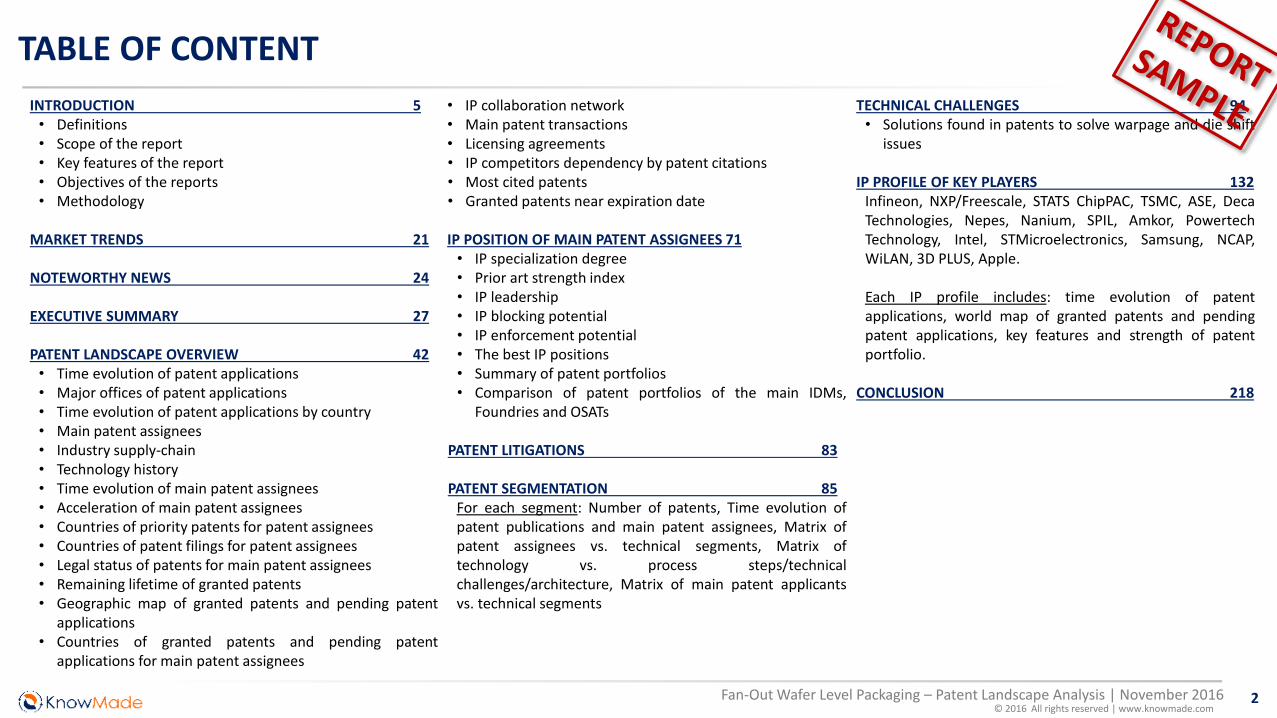
INTRODUCTION 5• Definitions• Scope of the report• Key features of the report• Objectives of the reports• Methodology
MARKET TRENDS 21
NOTEWORTHY NEWS 24
EXECUTIVE SUMMARY 27
PATENT LANDSCAPE OVERVIEW 42• Time evolution of patent applications• Major offices of patent applications• Time evolution of patent applications by country• Main patent assignees• Industry supply-chain• Technology history• Time evolution of main patent assignees• Acceleration of main patent assignees• Countries of priority patents for patent assignees• Countries of patent filings for patent assignees• Legal status of patents for main patent assignees• Remaining lifetime of granted patents• Geographic map of granted patents and pending patent
applications• Countries of granted patents and pending patent
applications for main patent assignees
• IP collaboration network• Main patent transactions• Licensing agreements• IP competitors dependency by patent citations• Most cited patents• Granted patents near expiration date
IP POSITION OF MAIN PATENT ASSIGNEES 71• IP specialization degree• Prior art strength index• IP leadership• IP blocking potential• IP enforcement potential• The best IP positions• Summary of patent portfolios• Comparison of patent portfolios of the main IDMs,
Foundries and OSATs
PATENT LITIGATIONS 83
PATENT SEGMENTATION 85For each segment: Number of patents, Time evolution ofpatent publications and main patent assignees, Matrix ofpatent assignees vs. technical segments, Matrix oftechnology vs. process steps/technicalchallenges/architecture, Matrix of main patent applicantsvs. technical segments
TECHNICAL CHALLENGES 94• Solutions found in patents to solve warpage and die shift
issues
IP PROFILE OF KEY PLAYERS 132Infineon, NXP/Freescale, STATS ChipPAC, TSMC, ASE, DecaTechnologies, Nepes, Nanium, SPIL, Amkor, PowertechTechnology, Intel, STMicroelectronics, Samsung, NCAP,WiLAN, 3D PLUS, Apple.
Each IP profile includes: time evolution of patentapplications, world map of granted patents and pendingpatent applications, key features and strength of patentportfolio.
CONCLUSION 218
3© 2016 All rights reserved | www.knowmade.com
Fan-Out Wafer Level Packaging – Patent Landscape Analysis | November 2016
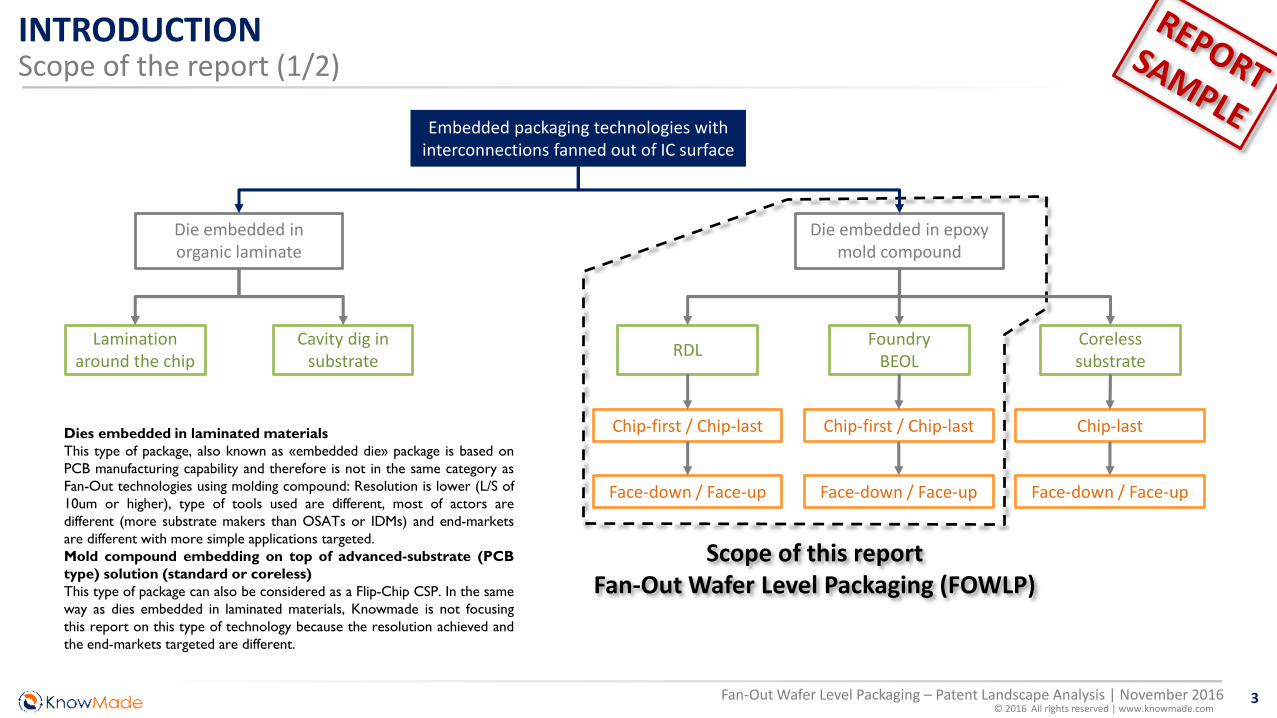
INTRODUCTIONScope of the report (1/2)
Die embedded in epoxy mold compound
RDLFoundry
BEOL
Die embedded in organic laminate
Lamination around the chip
Cavity dig in substrate
Coreless substrate
Chip-first / Chip-last
Face-down / Face-up
Chip-first / Chip-last
Face-down / Face-up
Chip-last
Face-down / Face-up
Embedded packaging technologies with interconnections fanned out of IC surface
Dies embedded in laminated materials
This type of package, also known as «embedded die» package is based on
PCB manufacturing capability and therefore is not in the same category as
Fan-Out technologies using molding compound: Resolution is lower (L/S of
10um or higher), type of tools used are different, most of actors are
different (more substrate makers than OSATs or IDMs) and end-markets
are different with more simple applications targeted.
Mold compound embedding on top of advanced-substrate (PCB
type) solution (standard or coreless)
This type of package can also be considered as a Flip-Chip CSP. In the same
way as dies embedded in laminated materials, Knowmade is not focusing
this report on this type of technology because the resolution achieved and
the end-markets targeted are different.
Scope of this reportFan-Out Wafer Level Packaging (FOWLP)
4© 2016 All rights reserved | www.knowmade.com
Fan-Out Wafer Level Packaging – Patent Landscape Analysis | November 2016
INTRODUCTIONScope of the report (2/2)
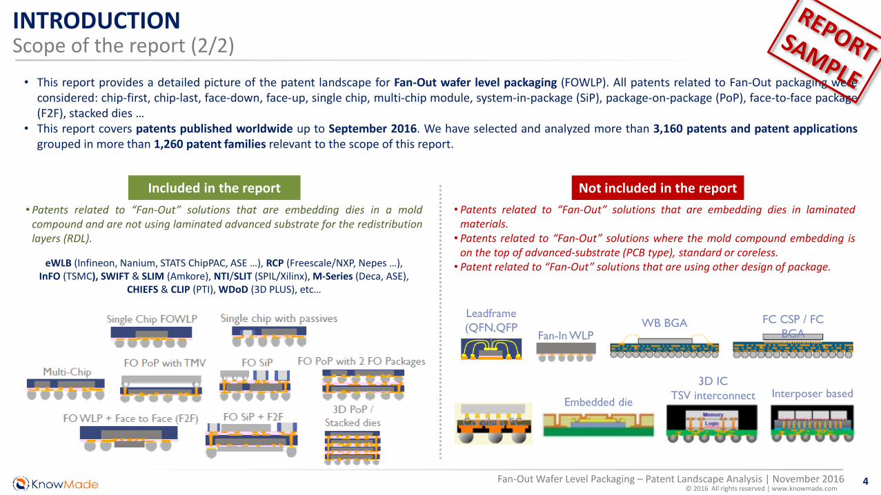
• This report provides a detailed picture of the patent landscape for Fan-Out wafer level packaging (FOWLP). All patents related to Fan-Out packaging wereconsidered: chip-first, chip-last, face-down, face-up, single chip, multi-chip module, system-in-package (SiP), package-on-package (PoP), face-to-face package(F2F), stacked dies …
• This report covers patents published worldwide up to September 2016. We have selected and analyzed more than 3,160 patents and patent applicationsgrouped in more than 1,260 patent families relevant to the scope of this report.
Included in the report Not included in the report
• Patents related to “Fan-Out” solutions that are embedding dies in laminatedmaterials.• Patents related to “Fan-Out” solutions where the mold compound embedding is
on the top of advanced-substrate (PCB type), standard or coreless.• Patent related to “Fan-Out” solutions that are using other design of package.
• Patents related to “Fan-Out” solutions that are embedding dies in a moldcompound and are not using laminated advanced substrate for the redistributionlayers (RDL).
eWLB (Infineon, Nanium, STATS ChipPAC, ASE …), RCP (Freescale/NXP, Nepes …), InFO (TSMC), SWIFT & SLIM (Amkore), NTI/SLIT (SPIL/Xilinx), M-Series (Deca, ASE),
CHIEFS & CLIP (PTI), WDoD (3D PLUS), etc…
Fan-In WLP
Leadframe
(QFN,QFP
)
WB BGA FC CSP / FC
BGA
3D IC
TSV interconnect Interposer basedEmbedded die
Coreless FC

5© 2016 All rights reserved | www.knowmade.com
Fan-Out Wafer Level Packaging – Patent Landscape Analysis | November 2016
INTRODUCTIONKey features of the report (1/2)
• The report provides essential patent data for Fan-Out wafer level packaging (chip-first, chip-last, face-down, face-up, single chip, multi-chip module, SiP, PoP, etc…).
• It provides in-depth patent analyses of key technologies and key players including:
– IP trends including time evolutions and countries of patent filings.
– Current legal status of patents.
– Ranking of main patent applicants.
– IP collaborations, joint developments and licensing agreements.
– IP position of key players and relative strength of their patent portfolios.
– Segmentation of patents by technology solution (chip-first/face-down, chip-first/face-up, chip-last), process steps (die placement,molding, planarization, RDL …), architecture (multi-chip module, PoP, SiP, face-to-face package …), technical challenge (warpage,die shift).
– Matrix showing patent applicants and their patented technologies.
– Technical solutions found in patents for warpage and die-shift issues.
• The “Fan-Out” IP profiles of 18 key companies is presented, including countries of filings, legal status of patents, patented technologies,prior-art strength index, IP blocking potential, partnerships and IP strategy: Infineon, NXP/Freescale, STATS ChipPAC, TSMC, ASE, DecaTechnologies, Nepes, Nanium, SPIL, Amkor, Powertech Technology, Intel, STMicroelectronics, Samsung, NCAP, WiLAN, 3D PLUS, Apple
6© 2016 All rights reserved | www.knowmade.com
Fan-Out Wafer Level Packaging – Patent Landscape Analysis | November 2016
INTRODUCTIONKey features of the report (2/2)
• The report also provides an extensive Excel database with all patents analyzed in the report (3,100+ patents), including technologysegmentation.
• This useful patent database allows multi-criteria searches, including:
- Patent publication number
- Hyperlinks to the original documents
- Priority date
- Title
- Abstract
- Patent assignees
- Technical segmentation (chip-first/face-down, chip-first/face-up, chip-last, die placement, molding, planarization, RDL … multi-chipmodule, PoP, SiP, face-to-face package … warpage, die shift).
- Legal status for each member of the patent family
• Disclaimer: This report does not provide any insight analyses or counsel regarding legal aspects or the validity of any individual patent.KNOWMADE is a research firm that provides technical analysis and technical opinions. KNOWMADE is not a law firm. The research,technical analysis and/or work proposed or provided by KNOWMADE and contained herein is not a legal opinion and should not beconstrued as such.
7© 2016 All rights reserved | www.knowmade.com
Fan-Out Wafer Level Packaging – Patent Landscape Analysis | November 2016
INTRODUCTIONObjectives of the report
Understand the competitive environment from technology and patent perspective
Understand technology & market from a patent perspective.Understand the patent landscape. Identify risks & opportunities.Comprehend key trends in IP and technology development.List the major players and the relative strength of their patent portfolio.Name new players. Identify IP collaboration networks between key players (industrial and academic).Position key players within the value chain and understand their strategic decisions.Understand the competitive landscape, your current and future competitors.Understand your competitors’ strategic direction and future product offerings.Determine your competitors’ strengths and weaknesses. Identify current legal status of patented technologies. Identify key patents by assignees and technology. Identify blocking and valuable patents.Overview of past and current litigations and licensing agreements.Avoid patent infringement.Appreciate the link between the patent landscape and market evolutions.Discover new markets & technology directions. Identify untapped areas and opportunities to direct R&D and patenting activity.
8© 2016 All rights reserved | www.knowmade.com
Fan-Out Wafer Level Packaging – Patent Landscape Analysis | November 2016
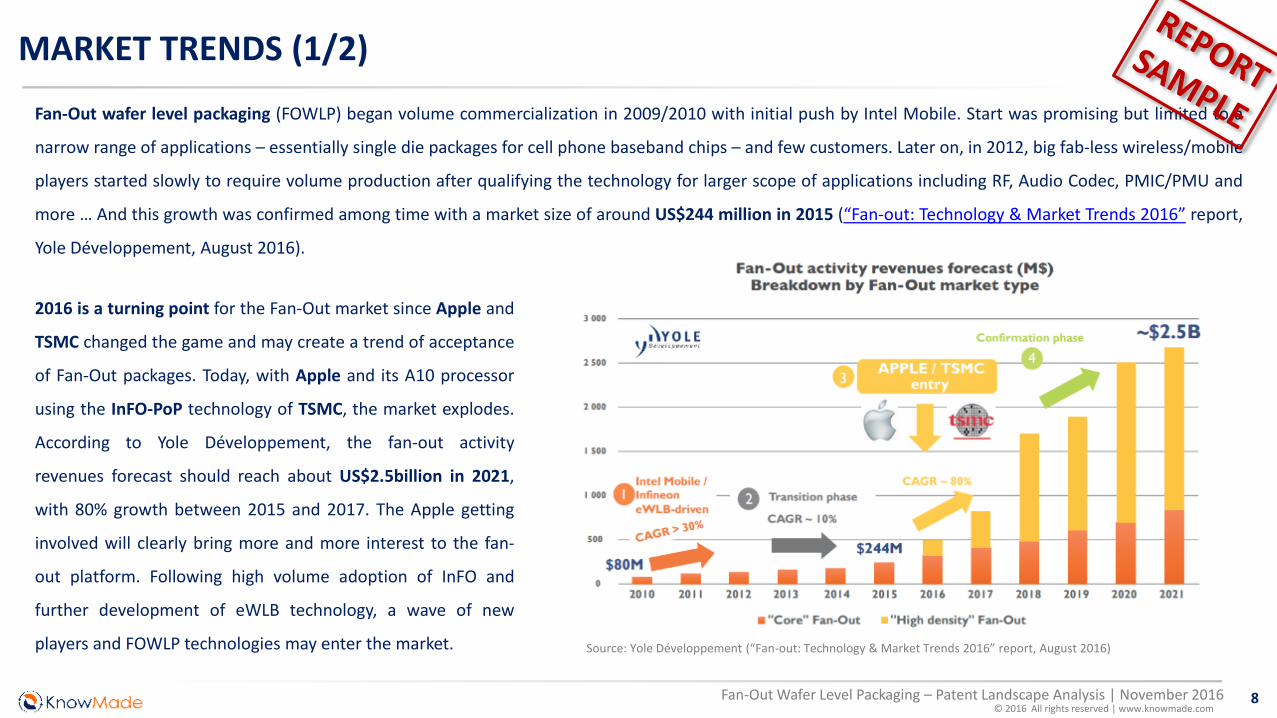
MARKET TRENDS (1/2)
Fan-Out wafer level packaging (FOWLP) began volume commercialization in 2009/2010 with initial push by Intel Mobile. Start was promising but limited to a
narrow range of applications – essentially single die packages for cell phone baseband chips – and few customers. Later on, in 2012, big fab-less wireless/mobile
players started slowly to require volume production after qualifying the technology for larger scope of applications including RF, Audio Codec, PMIC/PMU and
more … And this growth was confirmed among time with a market size of around US$244 million in 2015 (“Fan-out: Technology & Market Trends 2016” report,
Yole Développement, August 2016).
2016 is a turning point for the Fan-Out market since Apple and
TSMC changed the game and may create a trend of acceptance
of Fan-Out packages. Today, with Apple and its A10 processor
using the InFO-PoP technology of TSMC, the market explodes.
According to Yole Développement, the fan-out activity
revenues forecast should reach about US$2.5billion in 2021,
with 80% growth between 2015 and 2017. The Apple getting
involved will clearly bring more and more interest to the fan-
out platform. Following high volume adoption of InFO and
further development of eWLB technology, a wave of new
players and FOWLP technologies may enter the market. Source: Yole Développement (“Fan-out: Technology & Market Trends 2016” report, August 2016)

9© 2016 All rights reserved | www.knowmade.com
Fan-Out Wafer Level Packaging – Patent Landscape Analysis | November 2016
PATENT LANDSCAPE OVERVIEWTime evolution of patent applications for FOWLP
Patent activity in the field of fan-out wafer level packaging3,160+ patents (1,260+ patent families*), including 1,600+ granted patents and 1,200+ pending patent applications
Note: Due to thedelay between thefiling of patents andthe publications bypatent offices, usually18 months, the datacorresponding to theyear 2015 and 2016may not be completesince most patentsfiled during theseyears are notpublished yet.
* A patent family is a set
of patents filed in multiplecountries by a commoninventor(s) to protect asingle invention.
10© 2016 All rights reserved | www.knowmade.com
Fan-Out Wafer Level Packaging – Patent Landscape Analysis | November 2016
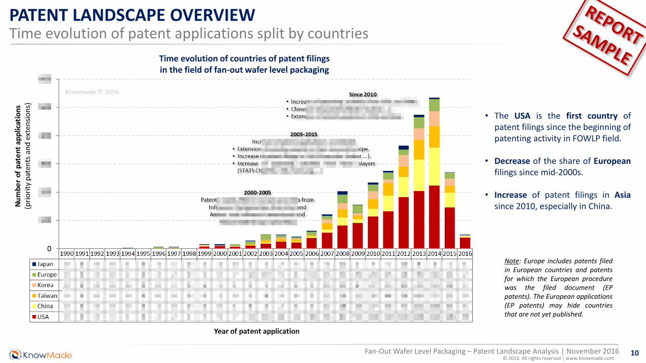
PATENT LANDSCAPE OVERVIEWTime evolution of patent applications split by countries
Time evolution of countries of patent filings in the field of fan-out wafer level packaging
• The USA is the first country ofpatent filings since the beginning ofpatenting activity in FOWLP field.
• Decrease of the share of Europeanfilings since mid-2000s.
• Increase of patent filings in Asiasince 2010, especially in China.
Note: Europe includes patents filedin European countries and patentsfor which the European procedurewas the filed document (EPpatents). The European applications(EP patents) may hide countriesthat are not yet published.
11© 2016 All rights reserved | www.knowmade.com
Fan-Out Wafer Level Packaging – Patent Landscape Analysis | November 2016
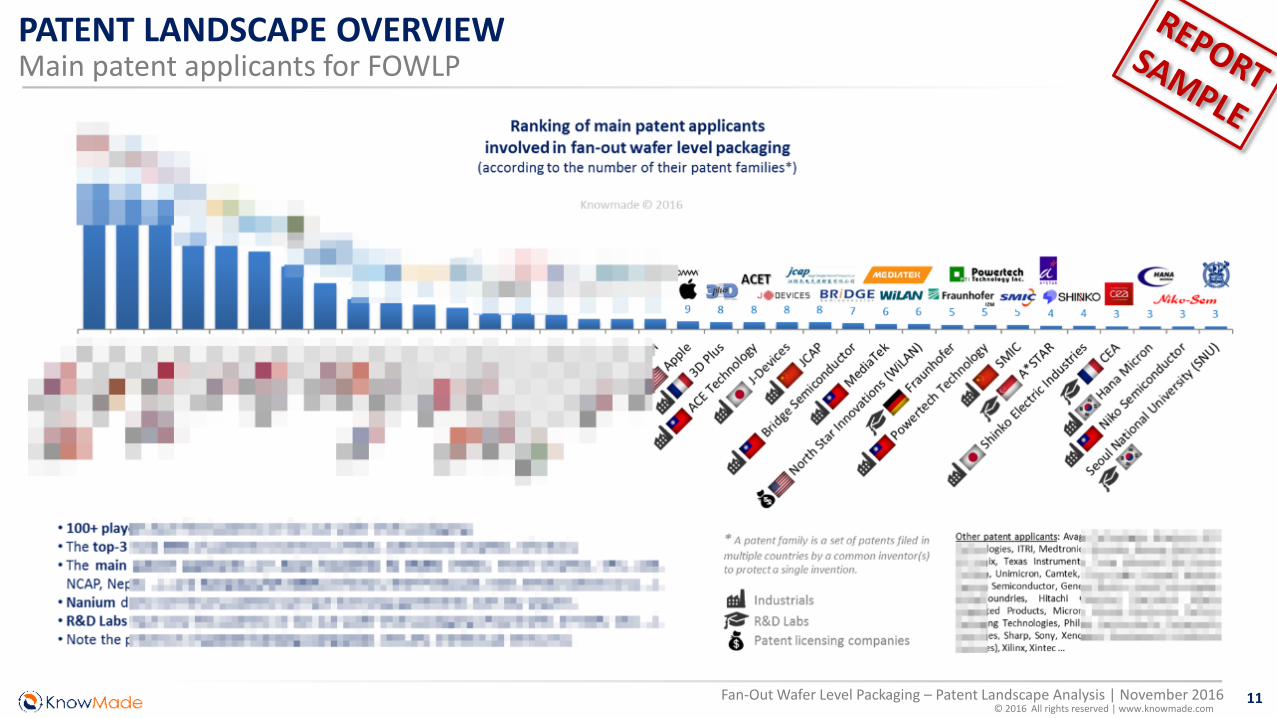
PATENT LANDSCAPE OVERVIEWMain patent applicants for FOWLP

12© 2016 All rights reserved | www.knowmade.com
Fan-Out Wafer Level Packaging – Patent Landscape Analysis | November 2016
PATENT LANDSCAPE OVERVIEWTime evolution of main patent assignees involved in FOWLP
* A patent family is a set of patents filed in multiple
countries by a common inventor(s) to protect a singleinvention.
Note: Due to the delay between the filing of patentsand the publications by patent offices, usually 18months, the data corresponding to the year 2015and 2016 may not be complete since most patentsfiled during these years are not published yet.
13© 2016 All rights reserved | www.knowmade.com
Fan-Out Wafer Level Packaging – Patent Landscape Analysis | November 2016
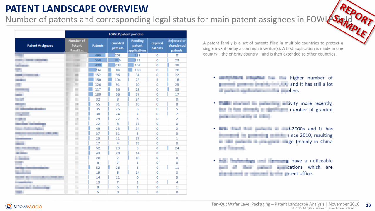
PATENT LANDSCAPE OVERVIEWNumber of patents and corresponding legal status for main patent assignees in FOWLP field

14© 2016 All rights reserved | www.knowmade.com
Fan-Out Wafer Level Packaging – Patent Landscape Analysis | November 2016
PATENT LANDSCAPE OVERVIEWRemaining lifetime of granted patents for main patent assignees in FOWLP field
15© 2016 All rights reserved | www.knowmade.com
Fan-Out Wafer Level Packaging – Patent Landscape Analysis | November 2016
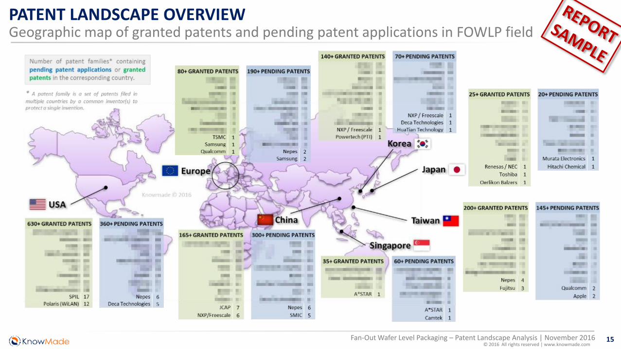
PATENT LANDSCAPE OVERVIEWGeographic map of granted patents and pending patent applications in FOWLP field

16© 2016 All rights reserved | www.knowmade.com
Fan-Out Wafer Level Packaging – Patent Landscape Analysis | November 2016
PATENT LANDSCAPE OVERVIEWCountries of granted patents and pending patent applications for main patent assignees in FOWLP field

17© 2016 All rights reserved | www.knowmade.com
Fan-Out Wafer Level Packaging – Patent Landscape Analysis | November 2016
PATENT LANDSCAPE OVERVIEWIP collaboration network in FOWLP field
• Number in black on each link between patent assignees is thenumber of co-assigned patent families in the data set of the study.
• Number up right to each bubble is the number of patent families forthis applicant in the data set of the study. Bubble size is proportionalto the number of patent families selected for the study.

18© 2016 All rights reserved | www.knowmade.com
Fan-Out Wafer Level Packaging – Patent Landscape Analysis | November 2016
PATENT LANDSCAPE OVERVIEWLicensing agreements
19© 2016 All rights reserved | www.knowmade.com
Fan-Out Wafer Level Packaging – Patent Landscape Analysis | November 2016
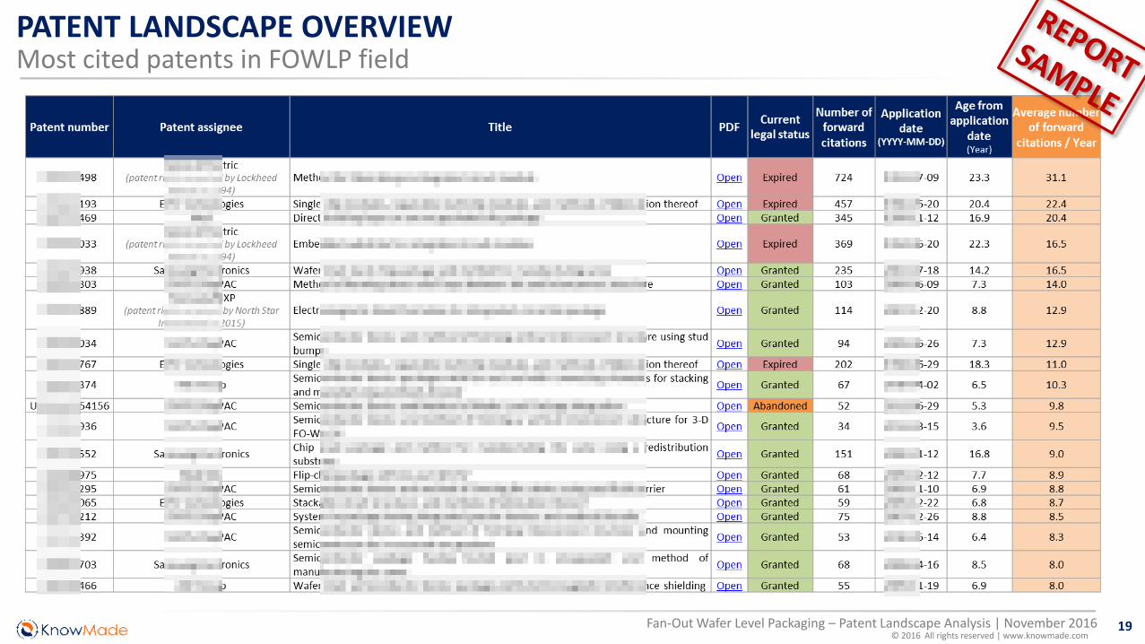
PATENT LANDSCAPE OVERVIEWMost cited patents in FOWLP field
20© 2016 All rights reserved | www.knowmade.com
Fan-Out Wafer Level Packaging – Patent Landscape Analysis | November 2016
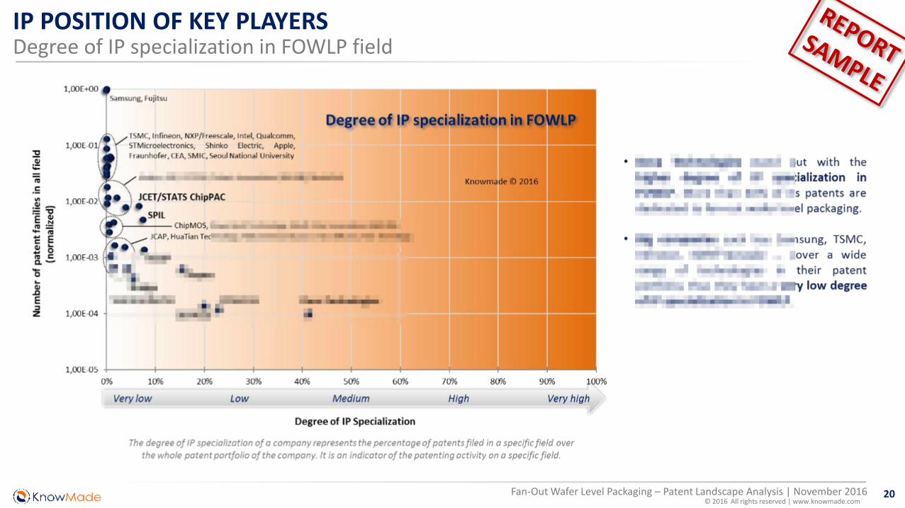
IP POSITION OF KEY PLAYERSDegree of IP specialization in FOWLP field

21© 2016 All rights reserved | www.knowmade.com
Fan-Out Wafer Level Packaging – Patent Landscape Analysis | November 2016
IP POSITION OF KEY PLAYERSPrior art strength index
(*) Internal citations refer to citationscoming from the corpus of patentsselected for the study. Externalcitations refer to citations comingfrom patents not selected for thestudy.
(**) A relative impact factor (R.I.F) of 2indicates that the patent portfolio is citedby two times more different patentfamilies than the average of the corpusselected for the study. In other terms, thepatent portfolio has two times moreimpact than the average.(***) Prior Art Strength Index = RelativeImpact Factor multiplied by the number ofpatent families.
The prior art strengthindex is based on thenumber of differentpatent families citing thepatent portfolio. Itindicates the impact ofthe patents on the priorart compared to otherpatents.

22© 2016 All rights reserved | www.knowmade.com
Fan-Out Wafer Level Packaging – Patent Landscape Analysis | November 2016
IP POSITION OF KEY PLAYERSPrior art strength index (citations from all technology fields)

23© 2016 All rights reserved | www.knowmade.com
Fan-Out Wafer Level Packaging – Patent Landscape Analysis | November 2016
IP POSITION OF KEY PLAYERSIP leadership in FOWLP field
24© 2016 All rights reserved | www.knowmade.com
Fan-Out Wafer Level Packaging – Patent Landscape Analysis | November 2016
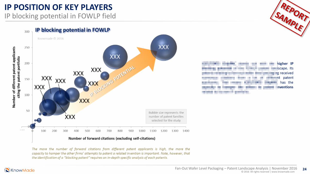
IP POSITION OF KEY PLAYERSIP blocking potential in FOWLP field
25© 2016 All rights reserved | www.knowmade.com
Fan-Out Wafer Level Packaging – Patent Landscape Analysis | November 2016
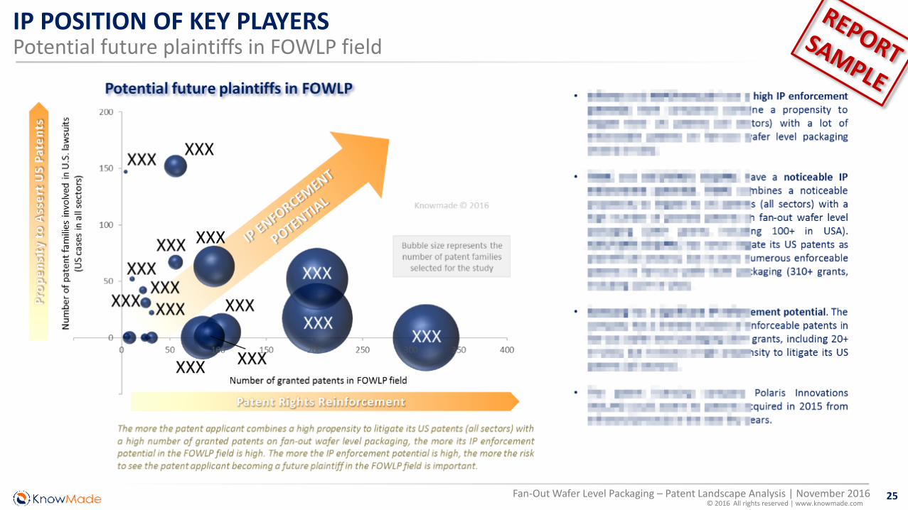
IP POSITION OF KEY PLAYERSPotential future plaintiffs in FOWLP field
26© 2016 All rights reserved | www.knowmade.com
Fan-Out Wafer Level Packaging – Patent Landscape Analysis | November 2016
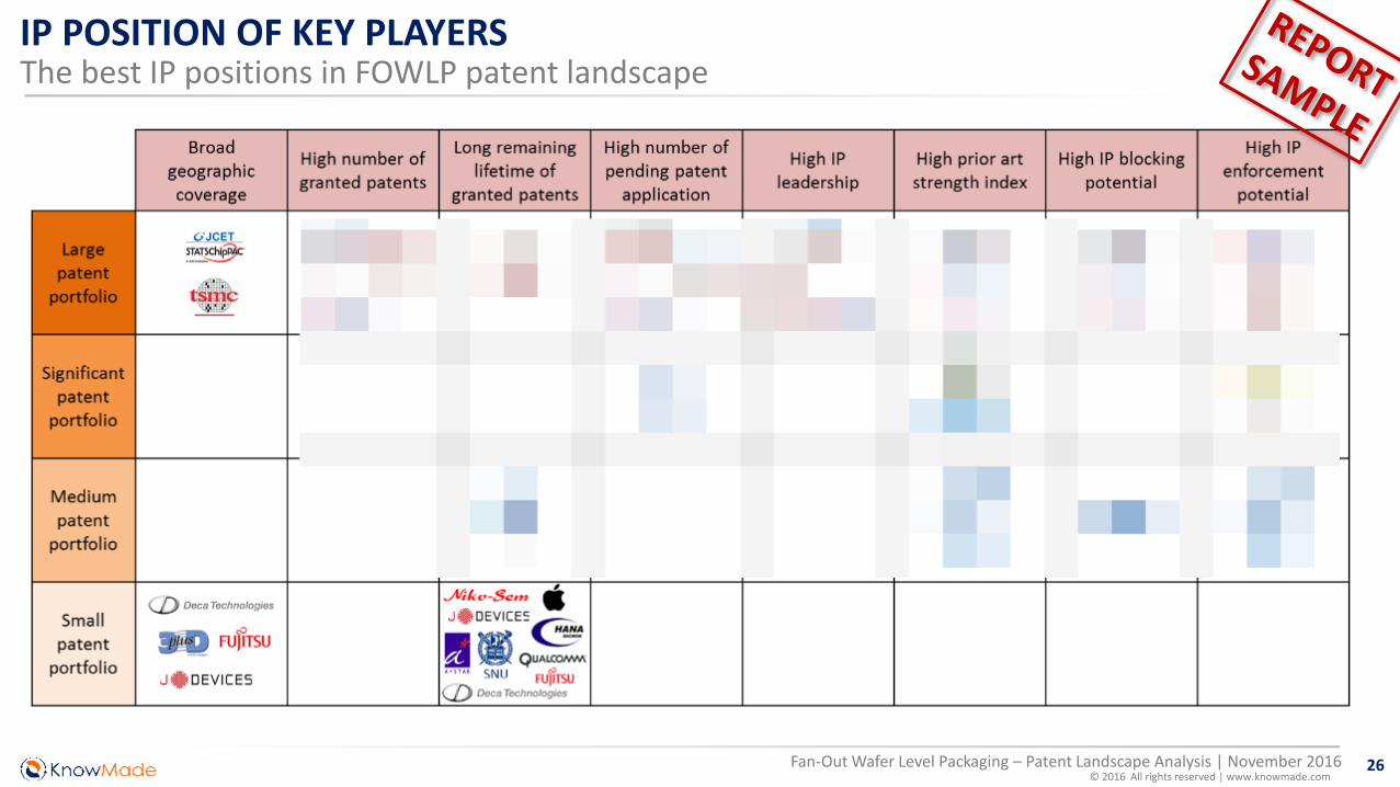
IP POSITION OF KEY PLAYERSThe best IP positions in FOWLP patent landscape

27© 2016 All rights reserved | www.knowmade.com
Fan-Out Wafer Level Packaging – Patent Landscape Analysis | November 2016
IP POSITION OF KEY PLAYERSSummary of patent portfolios
28© 2016 All rights reserved | www.knowmade.com
Fan-Out Wafer Level Packaging – Patent Landscape Analysis | November 2016
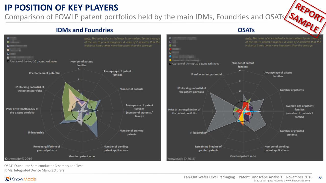
IP POSITION OF KEY PLAYERSComparison of FOWLP patent portfolios held by the main IDMs, Foundries and OSATs
OSAT: Outsource Semiconductor Assembly and TestIDMs: Integrated Device Manufacturers
29© 2016 All rights reserved | www.knowmade.com
Fan-Out Wafer Level Packaging – Patent Landscape Analysis | November 2016
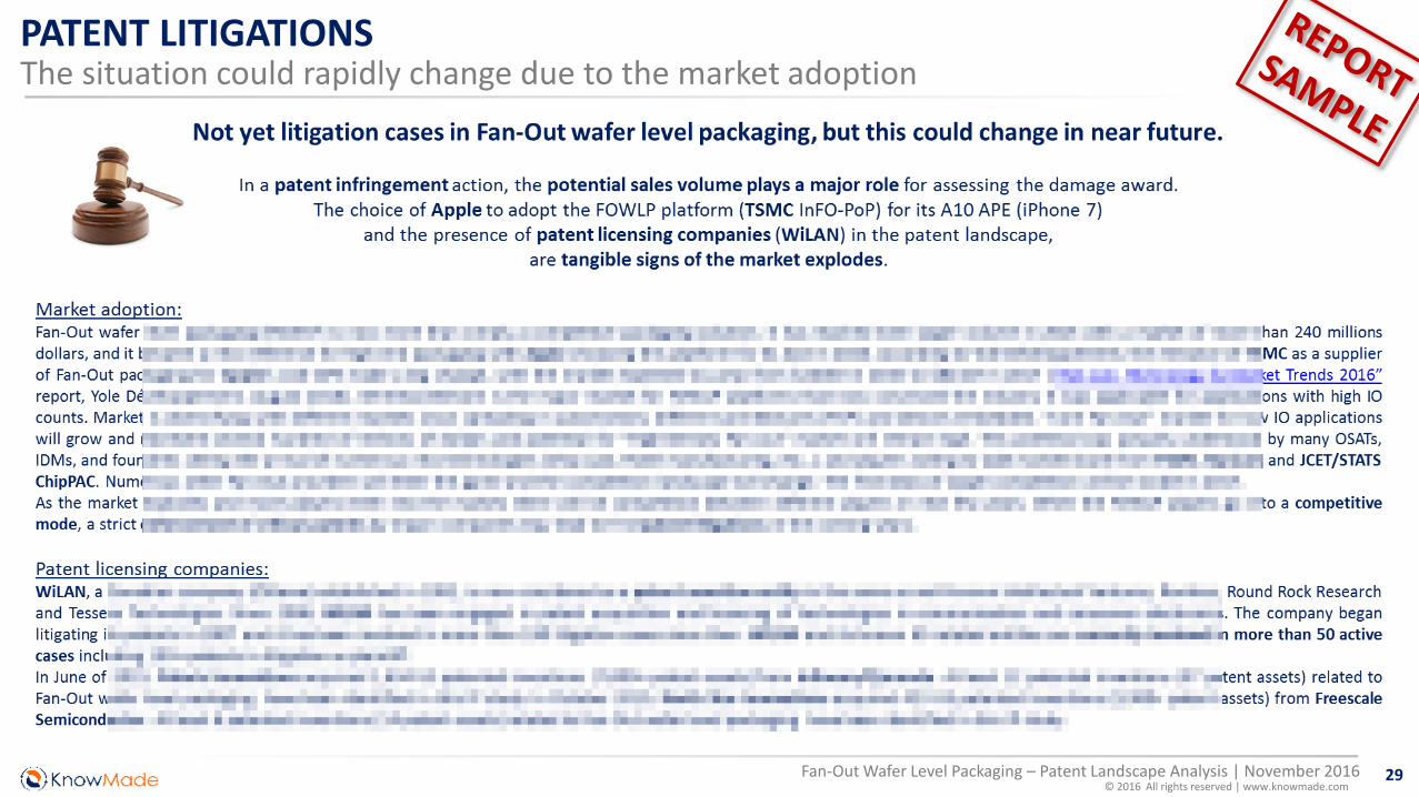
PATENT LITIGATIONSThe situation could rapidly change due to the market adoption

30© 2016 All rights reserved | www.knowmade.com
Fan-Out Wafer Level Packaging – Patent Landscape Analysis | November 2016
PATENT SEGMENTATIONNumber of patents, time evolution of patent publications and main patent assignees
31© 2016 All rights reserved | www.knowmade.com
Fan-Out Wafer Level Packaging – Patent Landscape Analysis | November 2016
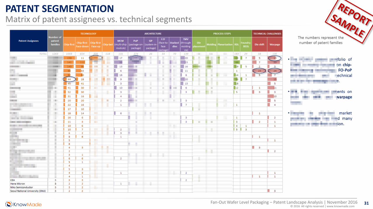
PATENT SEGMENTATIONMatrix of patent assignees vs. technical segments

32© 2016 All rights reserved | www.knowmade.com
Fan-Out Wafer Level Packaging – Patent Landscape Analysis | November 2016
PATENT SEGMENTATIONMatrix of technology vs. process steps/technical challenges/architecture
33© 2016 All rights reserved | www.knowmade.com
Fan-Out Wafer Level Packaging – Patent Landscape Analysis | November 2016
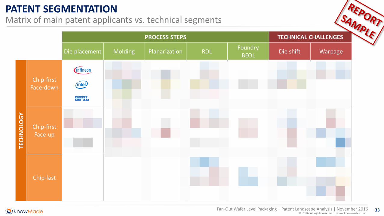
PATENT SEGMENTATIONMatrix of main patent applicants vs. technical segments

34© 2016 All rights reserved | www.knowmade.com
Fan-Out Wafer Level Packaging – Patent Landscape Analysis | November 2016
PATENT SEGMENTATIONMatrix of main patent applicants vs. technical segments
35© 2016 All rights reserved | www.knowmade.com
Fan-Out Wafer Level Packaging – Patent Landscape Analysis | November 2016
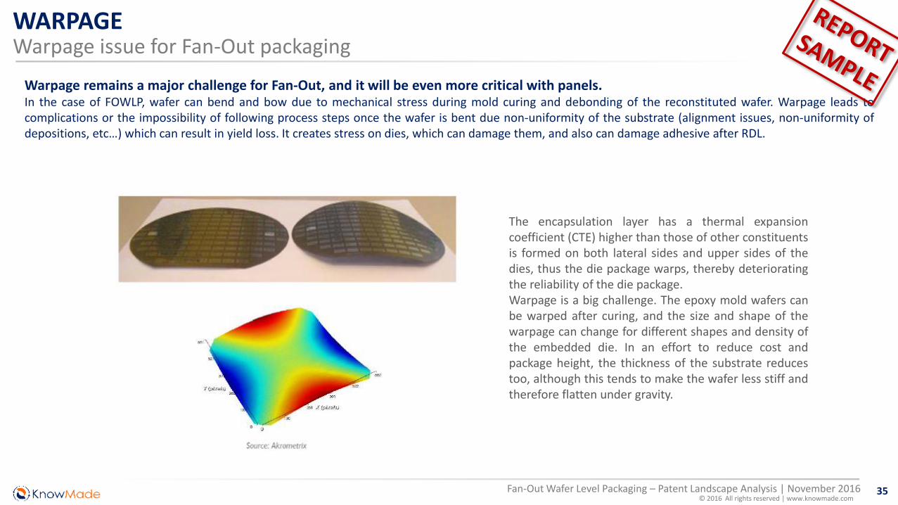
WARPAGEWarpage issue for Fan-Out packaging
Warpage remains a major challenge for Fan-Out, and it will be even more critical with panels.In the case of FOWLP, wafer can bend and bow due to mechanical stress during mold curing and debonding of the reconstituted wafer. Warpage leads tocomplications or the impossibility of following process steps once the wafer is bent due non-uniformity of the substrate (alignment issues, non-uniformity ofdepositions, etc…) which can result in yield loss. It creates stress on dies, which can damage them, and also can damage adhesive after RDL.
The encapsulation layer has a thermal expansioncoefficient (CTE) higher than those of other constituentsis formed on both lateral sides and upper sides of thedies, thus the die package warps, thereby deterioratingthe reliability of the die package.Warpage is a big challenge. The epoxy mold wafers canbe warped after curing, and the size and shape of thewarpage can change for different shapes and density ofthe embedded die. In an effort to reduce cost andpackage height, the thickness of the substrate reducestoo, although this tends to make the wafer less stiff andtherefore flatten under gravity.
36© 2016 All rights reserved | www.knowmade.com
Fan-Out Wafer Level Packaging – Patent Landscape Analysis | November 2016
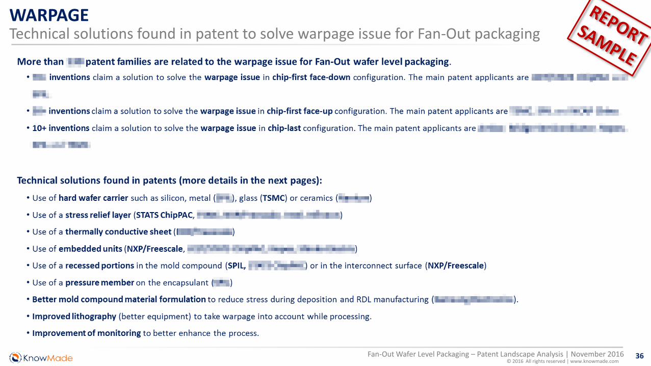
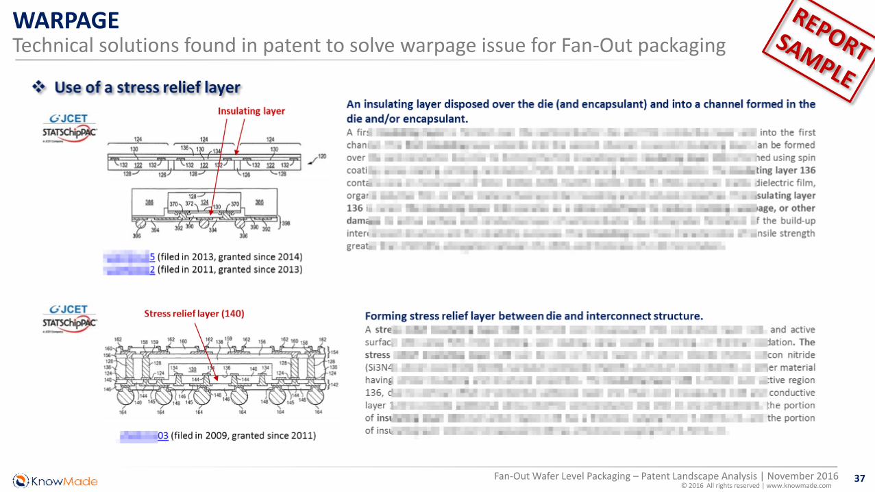
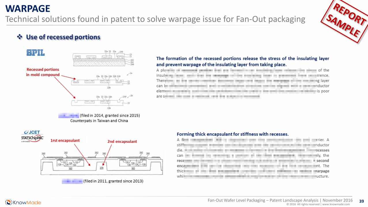
WARPAGETechnical solutions found in patent to solve warpage issue for Fan-Out packaging
37© 2016 All rights reserved | www.knowmade.com
Fan-Out Wafer Level Packaging – Patent Landscape Analysis | November 2016
WARPAGETechnical solutions found in patent to solve warpage issue for Fan-Out packaging

38© 2016 All rights reserved | www.knowmade.com
Fan-Out Wafer Level Packaging – Patent Landscape Analysis | November 2016
WARPAGETechnical solutions found in patent to solve warpage issue for Fan-Out packaging
39© 2016 All rights reserved | www.knowmade.com
Fan-Out Wafer Level Packaging – Patent Landscape Analysis | November 2016
WARPAGETechnical solutions found in patent to solve warpage issue for Fan-Out packaging

40© 2016 All rights reserved | www.knowmade.com
Fan-Out Wafer Level Packaging – Patent Landscape Analysis | November 2016
DIE SHIFTDie shift issue for chip-first Fan-Out packaging
Die shift during molding and mold curing is one of the major processing hurdles in chip-first FOWLP processes. It limits pitch capabilityand yield.Die shift is an unwanted movement of the chip after placing it on the carrier and depositing the molding. It results from shrinkage of the mold during curing. Itcan go up to several tens of microns. The consequence of die shift is an inaccurate alignments of die pads of reconfigured wafers which can cause yield losses.In case of multi-components FOWLP there can be die shifts in different directions within the same package. This is a critical issue which limits integrationcapability.
Source: Yole Développement
The thermal release tape is flexible. During amolding process, the coefficient of thermalexpansion (CTE) of the thermal release tapeand lateral forces from the encapsulant canlikely cause positional deviation of thesemiconductor chips (that is, positions of thesemiconductor chips are deviated from achip areas), thereby adversely affecting thepositional accuracy of the semiconductorchips. The larger the size of the carrier is, themore severe the positional deviation of thesemiconductor chips becomes. As such, theelectrical connection between theredistribution structure (RDL) and thesemiconductor chips is adversely affected,and consequently the product yield isreduced.
41© 2016 All rights reserved | www.knowmade.com
Fan-Out Wafer Level Packaging – Patent Landscape Analysis | November 2016
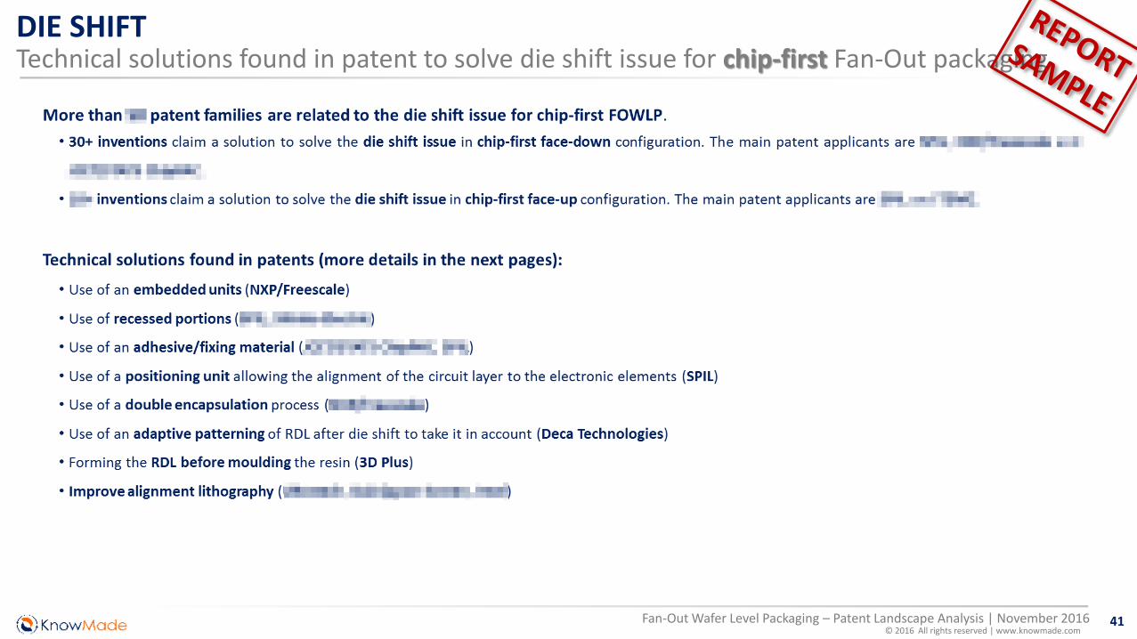
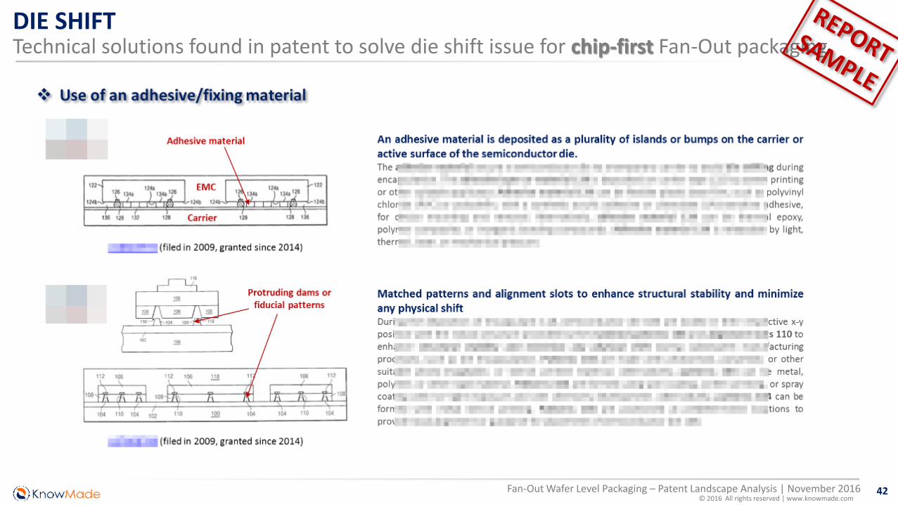
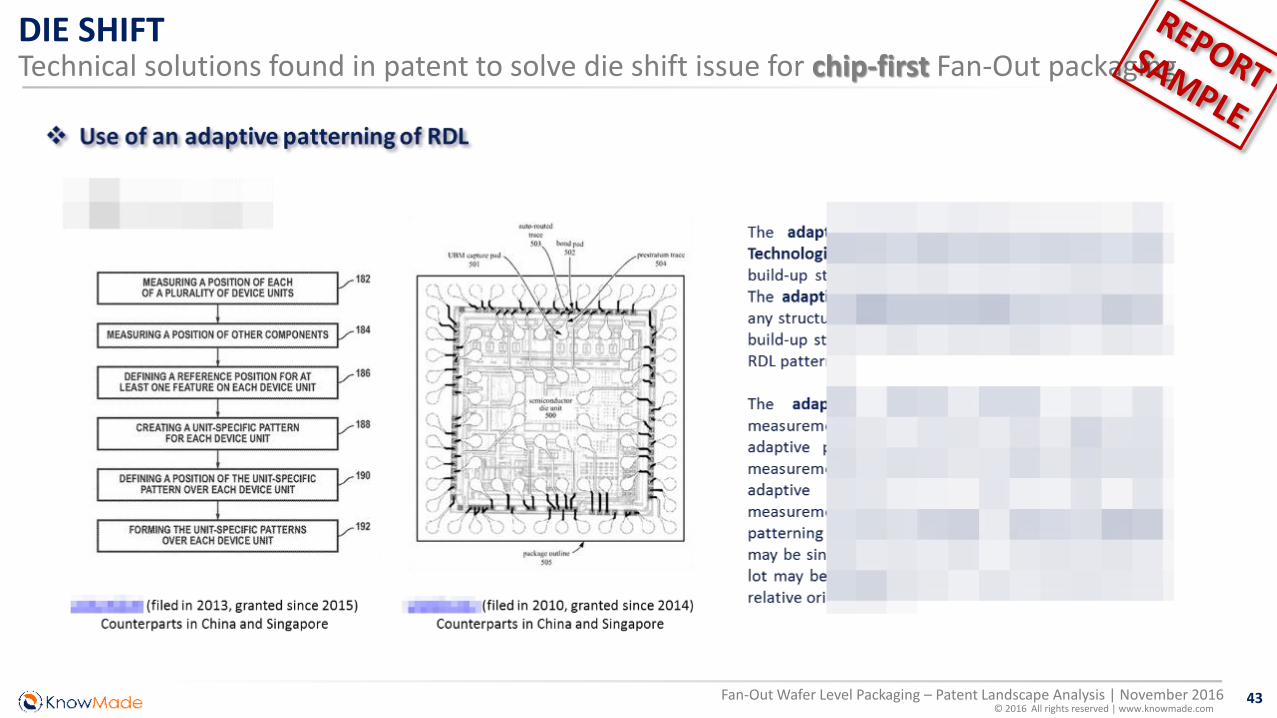
DIE SHIFTTechnical solutions found in patent to solve die shift issue for chip-first Fan-Out packaging
42© 2016 All rights reserved | www.knowmade.com
Fan-Out Wafer Level Packaging – Patent Landscape Analysis | November 2016
DIE SHIFTTechnical solutions found in patent to solve die shift issue for chip-first Fan-Out packaging
43© 2016 All rights reserved | www.knowmade.com
Fan-Out Wafer Level Packaging – Patent Landscape Analysis | November 2016
DIE SHIFTTechnical solutions found in patent to solve die shift issue for chip-first Fan-Out packaging
© 2016 All rights reserved | www.knowmade.com
IP PROFILE OF KEY PLAYERS

45© 2016 All rights reserved | www.knowmade.com
Fan-Out Wafer Level Packaging – Patent Landscape Analysis | November 2016
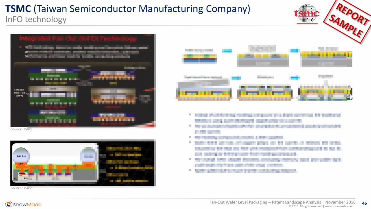
TSMC (Taiwan Semiconductor Manufacturing Company)InFO technology
46© 2016 All rights reserved | www.knowmade.com
Fan-Out Wafer Level Packaging – Patent Landscape Analysis | November 2016
TSMC (Taiwan Semiconductor Manufacturing Company)InFO technology
47© 2016 All rights reserved | www.knowmade.com
Fan-Out Wafer Level Packaging – Patent Landscape Analysis | November 2016
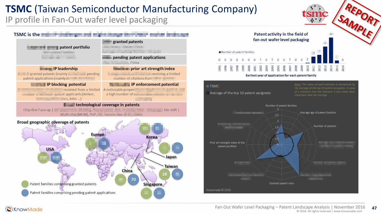
TSMC (Taiwan Semiconductor Manufacturing Company)IP profile in Fan-Out wafer level packaging
48© 2016 All rights reserved | www.knowmade.com
Fan-Out Wafer Level Packaging – Patent Landscape Analysis | November 2016
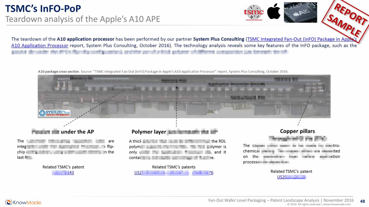
TSMC’s InFO-PoPTeardown analysis of the Apple’s A10 APE
49© 2016 All rights reserved | www.knowmade.com
Fan-Out Wafer Level Packaging – Patent Landscape Analysis | November 2016
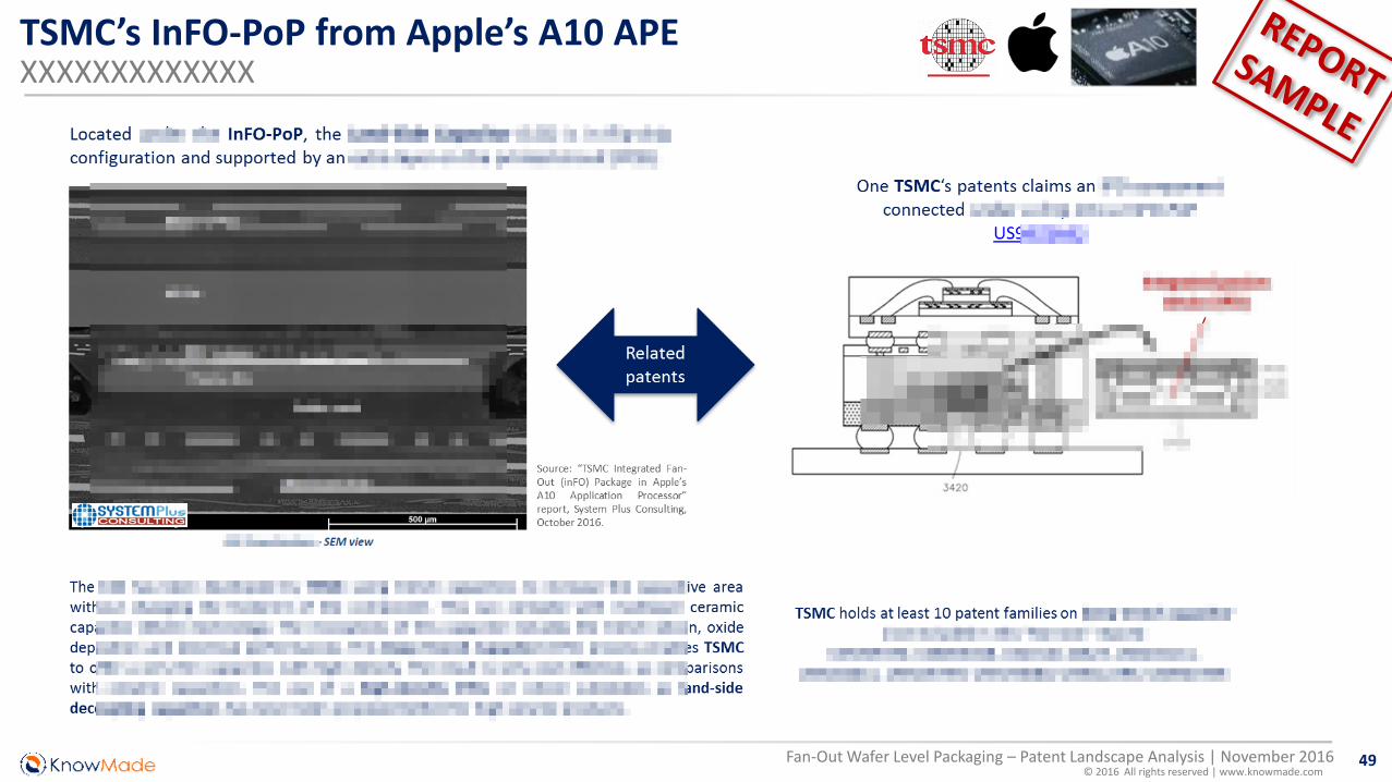
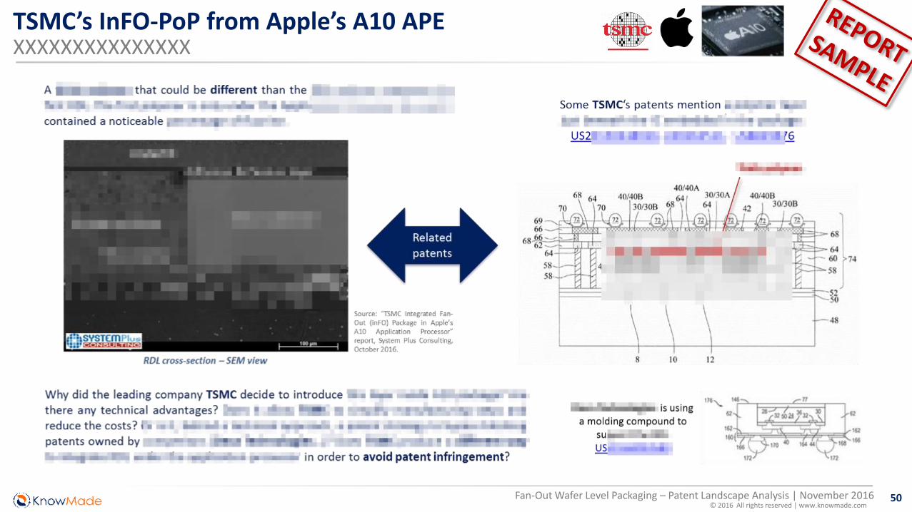
TSMC’s InFO-PoP from Apple’s A10 APEXXXXXXXXXXXXX
50© 2016 All rights reserved | www.knowmade.com
Fan-Out Wafer Level Packaging – Patent Landscape Analysis | November 2016
TSMC’s InFO-PoP from Apple’s A10 APEXXXXXXXXXXXXXXX
51© 2016 All rights reserved | www.knowmade.com
Fan-Out Wafer Level Packaging – Patent Landscape Analysis | November 2016
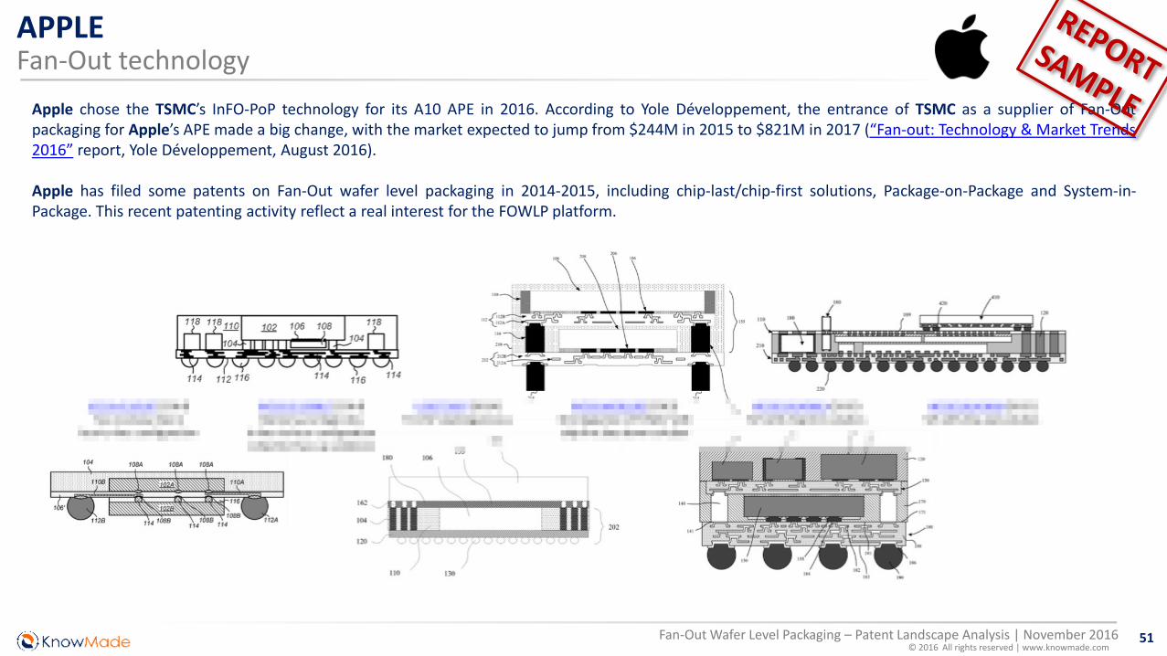
APPLEFan-Out technology
Apple chose the TSMC’s InFO-PoP technology for its A10 APE in 2016. According to Yole Développement, the entrance of TSMC as a supplier of Fan-Outpackaging for Apple’s APE made a big change, with the market expected to jump from $244M in 2015 to $821M in 2017 (“Fan-out: Technology & Market Trends2016” report, Yole Développement, August 2016).
Apple has filed some patents on Fan-Out wafer level packaging in 2014-2015, including chip-last/chip-first solutions, Package-on-Package and System-in-Package. This recent patenting activity reflect a real interest for the FOWLP platform.
52© 2016 All rights reserved | www.knowmade.com
Fan-Out Wafer Level Packaging – Patent Landscape Analysis | November 2016
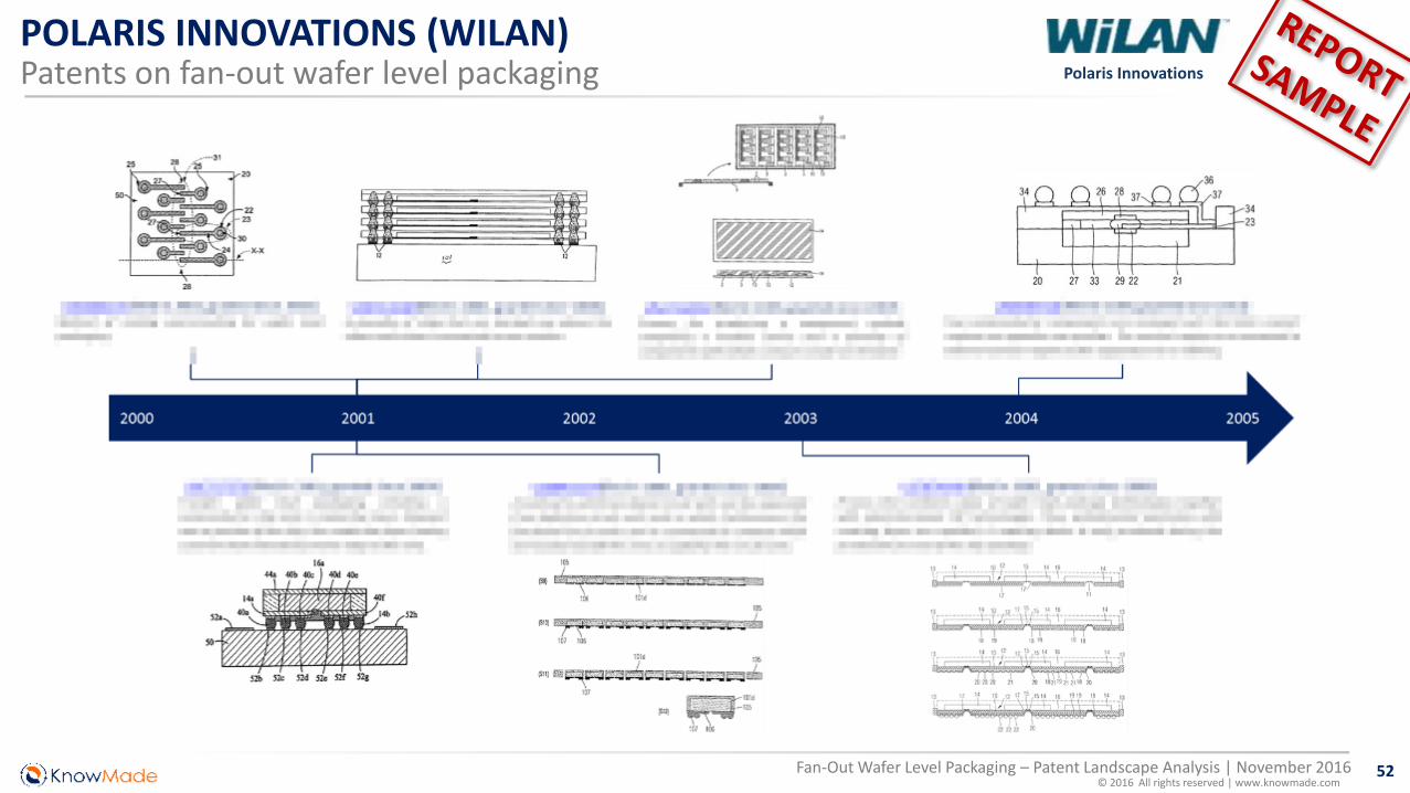
POLARIS INNOVATIONS (WILAN)Patents on fan-out wafer level packaging Polaris Innovations
53© 2016 All rights reserved | www.knowmade.com
Fan-Out Wafer Level Packaging – Patent Landscape Analysis | November 2016
CONTACT
o Consulting and Specific Analysis
– North America: Steve LaFerriere, Director of Northern America Business Development, Yole Inc.Email: [email protected]
– Europe: Lizzie Levenez, Europe Middle East and Africa Business Development Manager, Yole DéveloppementEmail: [email protected]
– Japan: Takashi Onozawa, General Manager, Yole Japan & President, Yole K.K.Email: [email protected]
– RoW: Jean-Christophe Eloy, President & CEO, Yole DéveloppementEmail: [email protected]
o Report business
– North America: Steve LaFerriere, Director of Northern America Business Development, Yole Inc.Email: [email protected]
– Europe: Fayçal El Khamassi, Headquarter Sales Coordination & Customer Service Email: [email protected]
– Japan & Asia: Takashi Onozawa, Sales Asia & General Manager, Yole K.K.Email: [email protected]
o Financial services
– Jean-Christophe Eloy, CEO & PresidentEmail: [email protected]
o General: Email: [email protected]