Paper TC357 Analytical Study of Substrate Parasitic ... · effects on SiGe HBT amplifiers in both...
12
Journal of Microwaves, Optoelectronics and Electromagnetic Applications, Vol. 12, No. 1, June 2013 Brazilian Microwave and Optoelectronics Society-SBMO received 26 Nov 2012; for review 29 Nov 2012; accepted 11 June 2013 Brazilian Society of Electromagnetism-SBMag © 2013 SBMO/SBMag ISSN 2179-1074 217 Abstract— An analytical study to quantify the substrate parasitic effects on SiGe HBT amplifiers in both common-base and common- emitter configuration is presented. The power gain relations and stability factors are derived from the modelled S-parameters which are computed at a fixed bias point from the small-signal hybrid-∏ model of SiGe HBT in both configurations. It has been shown that the power gains of SiGe HBT amplifiers in both configurations are degraded when extrinsic and substrate parasitics are taken into account. The degradation in power gains is found to be more pronounced for CB configuration, which makes the design of HBT amplifiers, particularly in the CB mode, difficult. Close matching of the modelled data with the reported experimental results validates the proposed methodology. Index Terms— Common-base, Common-emitter, Maximum Available Gain (MAG), Maximum Stable Gain (MSG), Scattering parameters, SiGe HBT, Stability factor, Substrate parasitics I. INTRODUCTION Recent technological developments in the area of SiGe heterojunction bipolar transistors (HBTs) have pushed the maximum oscillating frequency (f max ) and the current gain transition frequency (f t ) values into the millimeter wave range, which were unattainable with the conventional Si devices [1]. f max values close to 500GHz have been reported in literature [1]-[2]. Both single and multi-finger emitter configurations with high base doping coupled with the graded Ge base concentration yield high operating frequencies of SiGe HBTs [1]. It is known that many Monolithic Microwave Integrated Circuit (MMIC) foundries characterize the active and passive components based on s-parameter measurements. In addition to the s-parameter data, Mason’s unilateral power gain (U) gives information about the maximum oscillating frequency (f max ) of transistors, but the extracted f max from U doesn’t differ for the same transistor in different configurations, namely common base (CB) and common emitter (CE). Hence the power gain, G max (Maximum Available Gain/Maximum Stable gain) of transitor is widely used as a important figure of merit while comparing transistor performance in CE and CB configuration. The difference in power gain characteristics of SiGe HBT between the CE Analytical Study of Substrate Parasitic Effects in Common-Base and Common-Emitter SiGe HBT Amplifiers Neti V L Narasimha Murty * and M. Hemalata Rao School of Electrical Sciences, Indian Institute of Technology Bhubaneswar, Bhubaneswar-751013, INDIA [email protected]*and [email protected]
Transcript of Paper TC357 Analytical Study of Substrate Parasitic ... · effects on SiGe HBT amplifiers in both...

Journal of Microwaves, Optoelectronics and Electromagnetic Applications, Vol. 12, No. 1, June 2013
Brazilian Microwave and Optoelectronics Society-SBMO received 26 Nov 2012; for review 29 Nov 2012; accepted 11 June 2013
Brazilian Society of Electromagnetism-SBMag © 2013 SBMO/SBMag ISSN 2179-1074
217
Abstract— An analytical study to quantify the substrate parasitic
effects on SiGe HBT amplifiers in both common-base and common-
emitter configuration is presented. The power gain relations and
stability factors are derived from the modelled S-parameters which
are computed at a fixed bias point from the small-signal hybrid-∏
model of SiGe HBT in both configurations. It has been shown that
the power gains of SiGe HBT amplifiers in both configurations are
degraded when extrinsic and substrate parasitics are taken into
account. The degradation in power gains is found to be more
pronounced for CB configuration, which makes the design of HBT
amplifiers, particularly in the CB mode, difficult. Close matching of
the modelled data with the reported experimental results validates
the proposed methodology.
Index Terms— Common-base, Common-emitter, Maximum Available Gain
(MAG), Maximum Stable Gain (MSG), Scattering parameters, SiGe HBT,
Stability factor, Substrate parasitics
I. INTRODUCTION
Recent technological developments in the area of SiGe heterojunction bipolar transistors (HBTs) have
pushed the maximum oscillating frequency (fmax) and the current gain transition frequency (ft) values
into the millimeter wave range, which were unattainable with the conventional Si devices [1]. fmax
values close to 500GHz have been reported in literature [1]-[2]. Both single and multi-finger emitter
configurations with high base doping coupled with the graded Ge base concentration yield high
operating frequencies of SiGe HBTs [1]. It is known that many Monolithic Microwave Integrated
Circuit (MMIC) foundries characterize the active and passive components based on s-parameter
measurements. In addition to the s-parameter data, Mason’s unilateral power gain (U) gives
information about the maximum oscillating frequency (fmax) of transistors, but the extracted fmax from
U doesn’t differ for the same transistor in different configurations, namely common base (CB) and
common emitter (CE). Hence the power gain, Gmax (Maximum Available Gain/Maximum Stable gain)
of transitor is widely used as a important figure of merit while comparing transistor performance in
CE and CB configuration. The difference in power gain characteristics of SiGe HBT between the CE
Analytical Study of Substrate Parasitic Effects
in Common-Base and Common-Emitter SiGe
HBT Amplifiers
Neti V L Narasimha Murty* and M. Hemalata Rao
School of Electrical Sciences, Indian Institute of Technology Bhubaneswar, Bhubaneswar-751013, INDIA

Journal of Microwaves, Optoelectronics and Electromagnetic Applications, Vol. 12, No. 1, June 2013
Brazilian Microwave and Optoelectronics Society-SBMO received 26 Nov 2012; for review 29 Nov 2012; accepted 11 June 2013
Brazilian Society of Electromagnetism-SBMag © 2013 SBMO/SBMag ISSN 2179-1074
218
and CB configuration was studied by Ma et al. [3]. Their analytical model suggests that SiGe HBT
operated in CB configuration has higher Gmax than the CE configuration at higher operating
frequencies. They have attributed the superior gain performance of HBT in CB mode to the smaller
base resistance. Moreover, in SiGe technology the devices in an IC are isolated using deep trenches
on low resistive Si substrates. Eventhough, high resistive substrates are preferable for high frequency
applications, due to their complicated fabrication process (e.g. Float Zone-process vs standard
Czochralski Si growth), high-resistivity silicon wafers are quite expensive for commercial IC
applications [4]. Isolation in circuits realized on silicon substrates in fact is an outstanding topic
because a proper isolation technique is a key issue for complex circuits at high frequencies. Some
methods were proposed to improve the isolation among the devices integrated onto a monolithic chip
[5]. It has been reported that even with proper isolation techniques, substrate parasitics in HBT
degrade the performance of the electronic circuits mainly in low-power devices with smaller emitter
areas [6]-[7]. Since smaller emitter area (few emitter fingers) devices have low parasitic series
resitances compared to large area power devices and hence substrate coupling between and output
ports is more significant in few emitter finger HBTs. As the frequency of operation increases, the
influence of parasitic substrate effects becomes more important and must be taken into account for
accurate designing of HBT amplifiers. Several authors have attempted to modify the small-signal
equivalent circuit of HBT by including the substrate effects and have proposed direct parameter
extraction techniques from a large set of measured S-parameters for SiGe HBT biased in forward
active, cut-off and saturation regions [6], [7]-[10]. Huang et al. [7] have experimentally studied the
influence of substrate parasitic effects on power gains of SiGe HBT in both CB and CE
configurations. They have also carried out an analytical study using the modified hybrid-∏ model of
HBT with parasitic substarte capacitances. They have shown that the substrate parasitics indeed
deteriorate the maximum available gain of HBT, particularly in CB configuration. However, they
haven’t studied the effect of substrate parasitics on the stability of the HBT amplifiers. Recently, In
this paper we have presented a simple and analytical approach to study the effect of substrate
parasitics that couples input and output pads on the power gains of SiGe HBT amplifier in both
common-base and common-emitter configurations. For the analysis, we have started with the small-
signal hybrid-Π model reported by Lee [8] which is a the modified Gummel-Poon model with
parasitic elements Csub and Rsub . The extrinsic series resistances and inductances of the connecting
leads to base, emitter and collector terminals have been included in the complete-small signal
equivalent circuit of the HBT. Using the parameter conversions, S-parameters of the two-port HBT
amplifier in CB and CE mode have been computed for a matched impedance of 50 Ω. Later the
amplifier has been checked for stability in the frequency range of 1.2-50GHz at that bias point
including the above parasitic effects.The calculated values of the power gains in the frequency ranges
of 0.2 - 10GHz are in good agreement with the reported experimental results [8] in the literature.

Journal of Microwaves, Optoelectronics and Electromagnetic Applications, Vol. 12, No. 1, June 2013
Brazilian Microwave and Optoelectronics Society-SBMO received 26 Nov 2012; for review 29 Nov 2012; accepted 11 June 2013
Brazilian Society of Electromagnetism-SBMag © 2013 SBMO/SBMag ISSN 2179-1074
219
II. GAIN RELATIONS OF HBT AMPLIFIERS
A. Scattering Parameters
A simplified schematic structure of a SiGe HBT is shown in Fig.1 with the physical origin of
the lumped circuit elements. Most of the small-signal equivalent circuit models of active components
are derived from the measured Scattering parameters (S-parameters). Broadly they fall in two
categories: T-model and Hybrid Π - model. Each one of the above topologies has its own edge over the
other. All the model parameters of T-model can be directly derived from the device physics. Whereas
the hybrid-∏ model is the modified version of well-known Gummel-Poon model. Teeter et al. [10] has
compared both the circuit topologies of SiGe HBTs up to 100GHz. He has shown the direct
correspondence between these two models. He also concluded that the most often used hybrid-∏
model can be used for accurate circuit simulations with the inclusion of the collector current delay.
Fig. 1. Schematic structure of a SiGe HBT with the physical origin of lumped circuit intrinsic elements
Several authors have identified the parasitic substrate effects on the performance of SiGe
HBT amplifiers at high frequencies [5], [7-9]. They have modified the hybrid Π -model of HBT to
account for the substrate parasitics. In this study we have used the modified small-signal model
proposed by Lee [8] to include the substrate parasitic effects. Lee et al. have proposed an improved
parameter extraction method for Vertical Bipolar Inter Company (VBIC) -type hybrid Π- model of
SiGe HBTs by including a non-VBIC-parameter in the small-signal equivalent circuit. Their proposed
extraction method successfully characterizes the S-parameters of HBT for broad range of frequencies.
V -
+

Journal of Microwaves, Optoelectronics and Electromagnetic Applications, Vol. 12, No. 1, June 2013
Brazilian Microwave and Optoelectronics Society-SBMO received 26 Nov 2012; for review 29 Nov 2012; accepted 11 June 2013
Brazilian Society of Electromagnetism-SBMag © 2013 SBMO/SBMag ISSN 2179-1074
220
The small-signal equivalent circuit of the SiGe HBT is shown in Fig.2. Here Rb, Re and Rc are the
extrinsic parasitic resistances of the base, emitter and collector interconnection leads respectively. The
intrinsic device model of HBT is shown the inset of Fig. 2 in common emitter (CE) configuration.
The base-emitter (B-E) capacitance (Cbe) contains both diffusion and depletion capacitances of the B-
E junction whereas the base-collector capacitance (Cbc) includes only the depletion capacitance. The
transconductance (gm) contains a time delay component (τ) which changes the phase of S21-parameter
at high-frequencies and must be taken into account in calculating the power gains. The time delay (τ)
is actually the base-collector transit time, which is of the order of pico-seconds [8]. The parasitics due
to the substrate transistor action is included through Cbep, Csub and Rsub across the output terminals i.e.
collector –emitter [11]. Here Cbep is the parasitic capacitance associated with parasitic transistor action
of the base-collector-substrate junctions as defined in VBIC model [8]. Whereas, Csub and Rsub are
related to the substrate parameters of n+- p collector-substrate junction [6], [8]-[9]. Csco is a non-VBIC
parameter that accounts for small overlapping emitter-collector interconnection metals and its
associated capacitance, included by Lee [8].
Fig.2. Complete Small-signal model of SiGe HBT in common-emitter configuration. Inset of the figure shows the intrinsic
small-signal hybrid-∏ model of SiGe HBT.
Fig. 3. Complete Small-signal model of SiGe HBT in common-emitter configuration divided into four two-port networks
Cbc B1
Rbi
gm = gmo exp(-jwτcb)
V CbRbe
gmV
E1
C1
E1
Rb R
Re Rsub
Csub
Intrinsic hybrid
Π - Model of HBT B C
E
B1 C
1
E1
E
Csco
Cbep
Lb Lc
Le
Intrinsic HBT
Ze
E
B1
E1
E1
C1 C
Base
Zb Zc
Collector
Cbep
E
Rsub
Csub
Csco
Journal of Microwaves, Optoelectronics and Electromagnetic Applications, Vol. 12, No. 1, June 2013
Brazilian Microwave and Optoelectronics Society-SBMO received 26 Nov 2012; for review 29 Nov 2012; accepted 11 June 2013
Brazilian Society of Electromagnetism-SBMag © 2013 SBMO/SBMag ISSN 2179-1074
221
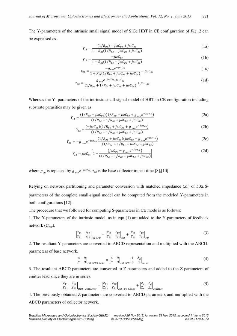
The Y-parameters of the intrinsic small signal model of SiGe HBT in CE configuration of Fig. 2 can
be expressed as
��� = �1 �⁄ � + ��� + ����1 + ���1 �⁄ + ��� + ����� (1a)
��� = −����1 + ���1 �⁄ + ��� + ����� (1b)
��� = −����������1 + ���1 �⁄ + ��� + ����� − ����
(1c)
��� = ���������� . �����1 � +⁄ 1 �� +⁄ ��� + ����� + ���� (1d)
Whereas the Y- parameters of the intrinsic small-signal model of HBT in CB configuration including
substrate parasitics may be given as
��� = �1 �⁄ + ����!1 � + ��� + ����������⁄ "�1 � +⁄ 1 �� +⁄ ��� + �����
(2a)
��� = �−�����!1 � + ��� + ����������⁄ "�1 � +⁄ 1 �� +⁄ ��� + �����
(2b)
��� = −���������� �1 �⁄ + �����!���� + ����������"�1 � +⁄ 1 �� +⁄ ��� + �����
(2c)
��� = ���� #1 − !���� − ����������"�1 � +⁄ 1 �� +⁄ ��� + �����$
(2d)
where ��is replaced by ����������. %� is the base-collector transit time [8],[10].
Relying on network partitioning and parameter conversion with matched impedance (Zo) of 50Ω, S-
parameters of the complete small-signal model can be computed from the modeled Y-parameters in
both configurations [12].
The procedure that we followed for computing S-parameters in CE mode is as follows:
1. The Y-parameters of the intrinsic model, as in eqn (1) are added to the Y-parameters of feedback
network (Cbep).
&��� ������ ���'()*+,- = &��� ������ ���'�)* + &��� ������ ���',- (3)
2. The resultant Y-parameters are converted to ABCD-representation and multiplied with the ABCD-
parameters of base network.
./ 0� 12()*+,-+34 = ./ 0� 12()*+,- .1 50 1 234 (4)
3. The resultant ABCD-parameters are converted to Z-parameters and added to the Z-parameters of
emitter lead since they are in series.
&5�� 5��5�� 5��'7-8���99�*�: = &5�� 5��5�� 5��'()*+,-+34 + &5 55 5'��**: (5)
4. The previously obtained Z-parameters are converted to ABCD-parameters and multiplied with the
ABCD parameters of collector network.

Journal of Microwaves, Optoelectronics and Electromagnetic Applications, Vol. 12, No. 1, June 2013
Brazilian Microwave and Optoelectronics Society-SBMO received 26 Nov 2012; for review 29 Nov 2012; accepted 11 June 2013
Brazilian Society of Electromagnetism-SBMag © 2013 SBMO/SBMag ISSN 2179-1074
222
./ 0� 127-8 = ./ 0� 127-8���99�*�: ./ 0� 12��99�*�: (6)
5. Finally, the ABCD parameters are converted to S-parameters with 50-Ω matched load [13]. Similarly the
S-parameters of HBT in CB mode are computed similar to the above procedure and using the intrinsic
Y-parameters of HBT (eqns (2a)-(2d)).
B. Power Gain calculations
Since the modeled S-parameters of HBT in both configurations are functions of the intrinsic elements,
extrinsic components and substrate parasitics through Rsub and Csub , the corresponding power gains
are strongly dependent on the above parameters particularly on the substrate parasitic for few-emitter
finger HBTs.
To evaluate the performance of SiGe HBT amplifiers, different definitions of power gains can
be used which are derived from the modeled S-parameters [12]. Stability of an amplifier is also
important if one wants to design it to work in low-frequency, high-gain regime. Stability factor (K) is
a parameter that gives information about the stability of the amplifier in the frequencies of interest
[14]. K can be determined from the S-parameters of the HBT as
; = 1 − |=��|� − |=��|� + |=��=�� − =��=��|2|=��||=��|
(7)
If K is greater than one, the amplifier is unconditionally stable (it will not oscillate for any impedance
present at input and output) and in this frequency regime where K>1, the maximum transducer power
gain (Gmax) of SiGe HBT amplifier is equal to Maximum Available Gain (MAG) is given by [13]
?�3@ = A/? = |=��||=��| B; − C;� − 1D
(8)
Whereas the Gmax of HBT when K<1 is equal to the Maximum Stable Gain (MSG) and is given by
[14]
?�3@ = A=? = |=��||=��| (9)
Mason’s unilateral gain (U) of the SiGe HBT can be calculated from the S-parameters by [14]
E = F=��=�� − 1F�
2. ;. F=��=��F − 2. �� B=��=��D
Where K is the stability factor expressed in eqn (7).
(10)
III. SIMULATION RESULTS AND DISCUSSION
Since S-parameters of HBT are bias and frequency dependent, we have computed the S-
parameters at a fixed bias i.e. for fixed intrinsic and extrinsic parameters for a fixed voltages and
currents [8]. For simplicity, we have used the extracted intrinsic and extrinsic parameters by Lee et al.
[8] which are Rbi = 8.56Ω, Cbep= 4.26fF, Csco= 15.2fF, Rbe = 2405Ω, Cbe= 0.465pF, gmo = 81mS, τcb =

Journal of Microwaves, Optoelectronics and Electromagnetic Applications, Vol. 12, No. 1, June 2013
Brazilian Microwave and Optoelectronics Society-SBMO received 26 Nov 2012; for review 29 Nov 2012; accepted 11 June 2013
Brazilian Society of Electromagnetism-SBMag © 2013 SBMO/SBMag ISSN 2179-1074
223
1.75ps, Cbc= 33.80fF, Csub = 23.93fF, Rsub= 1.926kΩ, Rb = 2.16Ω, Re = 1.91Ω, Rc=3.32 Ω and the parasitic
lead inductance values are Lb= 20pH, Le= 3.4pH and Lc= 22pH respectively.
The S-parameters of the SiGe HBT were computed using the lumped small-signal equivalent
circuit model of HBT, as in Fig. 2. The computed S-parameters at a fixed bias-point in CE
configuration using the above mentioned parameters is shown in Fig. 4 in the frequency range from
0.2-10.2 GHz. The modelled S-parameters qualitatively track the behavior reported in [8] typical to
HBT amplifiers. The effect of the substrate parasitics on the S-parameters of the SiGe HBT in CE
configuration is simulated and shown in Fig. 5. Note that the scaling factor of S21 parameter is much
lower than that of S12 parameter. As one can see, substrate parasitic effects severly degrade the S21
parameter (forward gain) of the HBT at higher frequencies. We have further computed |h21|2
and the
power gain (Gmax) using the modeled equations. Whereas, h21 is computed from the standard
parameter conversion from S-parameters to h-parameters [13]. As the frequency of operation
increases, Fig. 6 shows reduction in both the magnitude of square of h21 and Gmax which is attributed
to the presence of the frequency dependent parasitic elements. To check the valildity, we have
compared our modeled results with that of the reported experimental results of [8]. Very good
matching with the reported results complements the proposed methodology. Fig.7 compares the
intrinsic power gain of HBT amplifier in both CE and CB configuration, without extrinsic parasitic
elements in the frequency range from 1.2-50 GHz. The frequency of opertaions in the simulations has
been extended to further compare the gain improvements/degradation in one configuration compared
to the other. As evident from the results that the intrinsic HBT operated in CB configuration offers
improvement in the power gain which is expected because of the low base resistance (due to high base
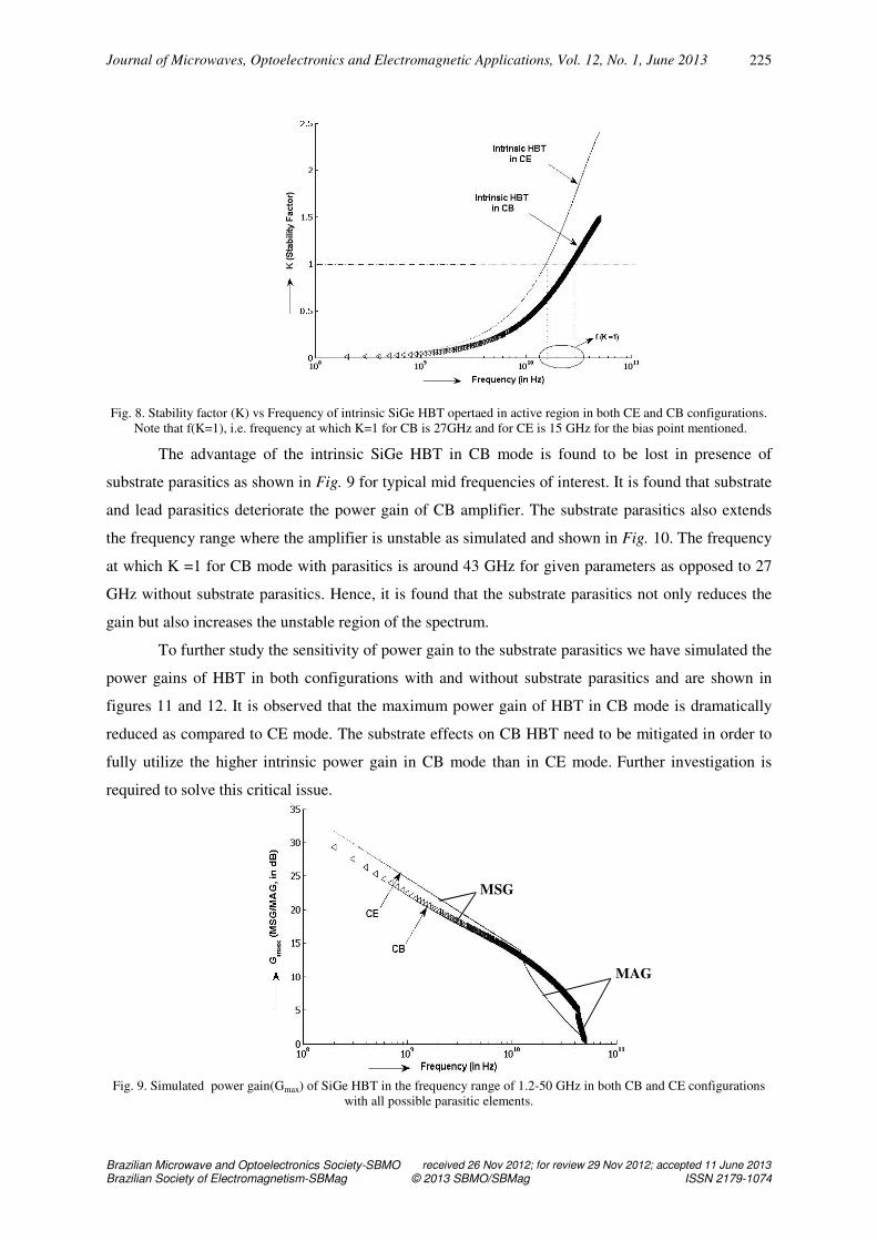
doping). The stability factor (K) of HBT amplifiers without parasitics in both CE and CB
configurations is also studied and is shown in Fig. 8. The frequency above which the amplifier is
stable is around 27GHz for CB mode and a lower value of around 15GHz for CE mode. It is evident
that the intrinsic HBT in common-base mode gives better gain and more stable than the corresponding
CE mode of operation.
Fig. 4. Simulated S-parameters of SiGe HBT in Common Emitter Configuration in the frequency range of 0.2-10 GHz.

Journal of Microwaves, Optoelectronics and Electromagnetic Applications, Vol. 12, No. 1, June 2013
Brazilian Microwave and Optoelectronics Society-SBMO received 26 Nov 2012; for review 29 Nov 2012; accepted 11 June 2013
Brazilian Society of Electromagnetism-SBMag © 2013 SBMO/SBMag ISSN 2179-1074
224
Fig. 5. Simulated S-parameters of SiGe HBT in the frequency range of 0.2-10 GHz with
substrate parasitics (black solid line) and without substrate parasitics (blue solid line).
Fig. 6. Calculated (−) and reported ( ) [8] |h21|2 and the power gain (Gmax) of SiGe HBT in the frequency range of 0.2-10 GHz.
Fig.7. Intrinsic power gain (Gmax)of a SiGe HBT opertaed in active region in both CE and CB configurations calculated in
the frequency range 1.2 – 50 GHz.
MS
G
MA
G
Journal of Microwaves, Optoelectronics and Electromagnetic Applications, Vol. 12, No. 1, June 2013
Brazilian Microwave and Optoelectronics Society-SBMO received 26 Nov 2012; for review 29 Nov 2012; accepted 11 June 2013
Brazilian Society of Electromagnetism-SBMag © 2013 SBMO/SBMag ISSN 2179-1074
225
Fig. 8. Stability factor (K) vs Frequency of intrinsic SiGe HBT opertaed in active region in both CE and CB configurations.
Note that f(K=1), i.e. frequency at which K=1 for CB is 27GHz and for CE is 15 GHz for the bias point mentioned.
The advantage of the intrinsic SiGe HBT in CB mode is found to be lost in presence of
substrate parasitics as shown in Fig. 9 for typical mid frequencies of interest. It is found that substrate
and lead parasitics deteriorate the power gain of CB amplifier. The substrate parasitics also extends
the frequency range where the amplifier is unstable as simulated and shown in Fig. 10. The frequency
at which K =1 for CB mode with parasitics is around 43 GHz for given parameters as opposed to 27
GHz without substrate parasitics. Hence, it is found that the substrate parasitics not only reduces the
gain but also increases the unstable region of the spectrum.
To further study the sensitivity of power gain to the substrate parasitics we have simulated the
power gains of HBT in both configurations with and without substrate parasitics and are shown in
figures 11 and 12. It is observed that the maximum power gain of HBT in CB mode is dramatically
reduced as compared to CE mode. The substrate effects on CB HBT need to be mitigated in order to
fully utilize the higher intrinsic power gain in CB mode than in CE mode. Further investigation is
required to solve this critical issue.
Fig. 9. Simulated power gain(Gmax) of SiGe HBT in the frequency range of 1.2-50 GHz in both CB and CE configurations
with all possible parasitic elements.
MSG
MAG

Journal of Microwaves, Optoelectronics and Electromagnetic Applications, Vol. 12, No. 1, June 2013
Brazilian Microwave and Optoelectronics Society-SBMO received 26 Nov 2012; for review 29 Nov 2012; accepted 11 June 2013
Brazilian Society of Electromagnetism-SBMag © 2013 SBMO/SBMag ISSN 2179-1074
226
Fig. 10. Stability factor for different frequencies of SiGe HBT in CE and CB configurations with parasitic elements.
f(K=1) for CB is around 43GHz and for CE is 14 GHz for the bias point mentioned.
Fig. 11 Simulated Gmax vs frequency of HBT in CE mode showing the effect of substrate parasitics in the frequency range
0.2-10.2 GHz.
Fig. 12 Variation of Power gain of SiGe HBT for different frequencies in the range 0.2-10.2 GHz with and without substrate
parasitics.

Journal of Microwaves, Optoelectronics and Electromagnetic Applications, Vol. 12, No. 1, June 2013
Brazilian Microwave and Optoelectronics Society-SBMO received 26 Nov 2012; for review 29 Nov 2012; accepted 11 June 2013
Brazilian Society of Electromagnetism-SBMag © 2013 SBMO/SBMag ISSN 2179-1074
227
It is well known that the transition frequency (ft) of a SiGe HBT is an important figure of
merit since it determines the operating frequency at which the common-emitter, short circuit current
gain (hfe) decreases to unity. The ft can be extracted by extrapolating |ℎ��|� Vs f curve (such as in
Fig.6) of the HBT. However, the operation of the HBT at higher frequencies above ft is still possible
beacuse of the gain available due to mismatch between input and output. The maximum frequency of
oscillation (fmax) is the frequency at which the power gain of a HBT drops to unity. The fmax of SiGe
HBT can also be derived based on unilateral gain, using eqn.10, by finding out the frequency at which
U=1. From practical standpoint, U is easier to measure at realtively low frequencies as compared to
MAG requires measurements upto higher frequencies. Moreover, the fmax extracted from U data is
always found to be higher than extracted from power gain (MAG) data, and hence is a natural choice
being used by many groups [15]. Hence, in order to study the effect of substrate parasitics on the
maximum oscillating frequency (fmax) of the SiGe HBT the variation of the calculated Mason’s
unilateral power gain (U) with frequency, calculated using eqn. (10), is plotted in Fig. 13. It is
observed that the unilateral gain (U) of the SiGe HBT decreases with increae in frequencies in both
cases. The value of fmax of the SiGe HBT without parasitics is found to be 70.65GHz where as the
substrate parasitics are found to reduce the fmax from 70.65GHz to 49GHz.
Fig. 13 Variation of Mason’s unilateral gain (U) of SiGe HBT for different frequencies in the range 0.2-100 GHz with and
without substrate parasitics. The extracted fmax from U without parasitics is found to be 70.65 GHz and fmax with parasitics is
approximately 49 GHz.
IV. CONCLUSIONS
In this paper, an improved and accurate analytical approach to study the effect of substrate parasitics
on the power gain relations of SiGe HBT in both CB and CE configurations was presented. The
methodology was based on modeling the S-parameters derived from the complete small-signal
hybrid-Π model of SiGe HBT including intrinsic, extrinsic and substrate parasitic elements. The
influence of substrate parasitics are simulated with the help of the modeled S-parameters. The power

Journal of Microwaves, Optoelectronics and Electromagnetic Applications, Vol. 12, No. 1, June 2013
Brazilian Microwave and Optoelectronics Society-SBMO received 26 Nov 2012; for review 29 Nov 2012; accepted 11 June 2013
Brazilian Society of Electromagnetism-SBMag © 2013 SBMO/SBMag ISSN 2179-1074
228
gains (MSG/MAG) of the SiGe HBT were calculated using the modeled S-parameters with and
without substrate parasitics analytically. The excellent agreement between modeled and experimental
work reported in literature has proven the accuracy of the proposed methodology. It is found that the
superior gain characteristics of intrinsic CB SiGe HBT amplifier over CE amplifier are lost in
presence of substrate parasitics. Substrate parasitic effects further increase the instability by reducing
the stability factor (K) for a given frequency in both configurations. Our simulation results showed
that this degradation is more pronounced for HBT operated in CB mode than in CE mode, which
makes the HBT design extremely in-efficient in CB mode than corresponding CE mode. Hence proper
care must be taken in designing HBT amplifiers particularly in the CB mode. It is also observed that
the parasitics in SiGe HBT degrade the maximum frequency of oscillation (fmax) in addition to the
unilateral gain (U). Other ways of minimizing the substrate effects need to be investigated.
REFERENCES
[1] B. Heinemann, A. Fox and H. Rücker, “Advanced transistor architectures for half-terahertz SiGe HBTs,” ECE Trans.,
vol.50, pp.61-71, 2013.
[2] P. Chevalier, T. F. Meister, B. Heinemann, S. Van Huylenbroeck, W. Liebl, A. Fox, A. Sibaja-Hernandez and A.
Chantre, “Towards THz SiGe HBTs,” IEEE Bipolar/BiCMOS Circuits and Technology Meeting (BCTM), 2011,
pp.5765.
[3] Z. Ma and N Jiang, “On the operation Configuration of SiGe HBTs based on power gain analysis,” IEEE Trans.
Electron Devices, vol. 52, pp. 248-255, 2005.
[4] J. Lee, Y. Kim, E. Lee, C. Kim and P. Roblin, “A 8-GHz SiGe HBT VCO design on a low resistive silicon substrate
using GSML,” IEEE Trans. Circuits. Syst. I, vol.54, pp.2128-2136, 2007.
[5] E. Sönmez, S. Chartier, A. Trasser and H. Schumacher, “ Isolation issues in multifunctional Si/SiGe ICs at 24GHz,” in
International Microwave Symposium, 2005, pp. 12-17.
[6] T. K. Johansen, J. Vidkjær and V. Krozer, “Substrate effects in SiGe HBT modeling,” in GaAs IC Symp. Tech. Dig.,
2003, pp.445-448.
[7] H. Huang, Z. Ma, P. Ma and M. Ranennelli, “Influence of substrate parasitic effects on power gain relation between CE
and CB SiGe HBTs,” in Silicon Monolithic Integrated Circuits in RF systems, 2008, pp. 62-65.
[8] K. Lee, K. Choi, S. Kook, D. Cho, K. park and B. Kim, “ Direct parameter extraction of SiGe HBTs for the VBIC
bipolar compact model,” IEEE Trans. Electron Devices, vol.52, pp.375-384, 2005.
[9] B. Han, H. Wang and J. Gao, “ An approach for SiGe HBT small-signal modeling up to 40 GHz,” Intl. Journal of
Electronics, 2013, DOI:10.1080/00207217.2013.769182.
[10] D. A. Teeter and W. R. Curtice, “Comparison of hybrid Pi and Tee HBT circuit topologies and their relationship to
large signal modeling,” in IEEE-MTT S Digest, 1997, pp.375-378.
[11] U. Basaran, N. Wieser, G. Feiler and M. Berroth, “Small-signal and high frequency noise modeling of SiGe HBTs,”
IEEE Tran. Microwave Theory and Tech., vol.53, pp.919-928, 2005.
[12] Neti V L Narasimha Murty and S. Jit,” Analytical modeling of photo-effects on s-parameters of GaAs MESFETs,”,
Microwave Optical Technol Lett, vol.48, pp. 150-155, 2006.
[13] S. Marsh, Practical MMIC Design, Boston: Artech House, 2006.
[14] R. Ludwig and G. Bogdanov, RF Circuit Design: Theory and Applications, New Jersey: Pearson Edu, 2009.
[15] J. D. Cressler and G. Niu, Silicon-Germanium Heterojunction Bipolar Transistors, Boston: Artech House, 2003.