LARGE-SIGNAL NETWORK ANALYZER … NETWORK ANALYZER MEASUREMENTS AND THEIR USE IN ... • tuning of...
24
Ewout Vandamme (Agilent Technologies, NMDG), Wladek Grabinski (Motorola, Geneva), Dominique Schreurs (K.U.Leuven), and Thomas Gneiting (ADMOS) LARGE-SIGNAL NETWORK ANALYZER MEASUREMENTS AND THEIR USE IN DEVICE MODELLING
Transcript of LARGE-SIGNAL NETWORK ANALYZER … NETWORK ANALYZER MEASUREMENTS AND THEIR USE IN ... • tuning of...

Ewout Vandamme (Agilent Technologies, NMDG),Wladek Grabinski (Motorola, Geneva),Dominique Schreurs (K.U.Leuven), andThomas Gneiting (ADMOS)
LARGE-SIGNAL NETWORK ANALYZER MEASUREMENTS AND THEIR USE IN
DEVICE MODELLING
Mixdes 2002© 2002, Agilent Technologies
2
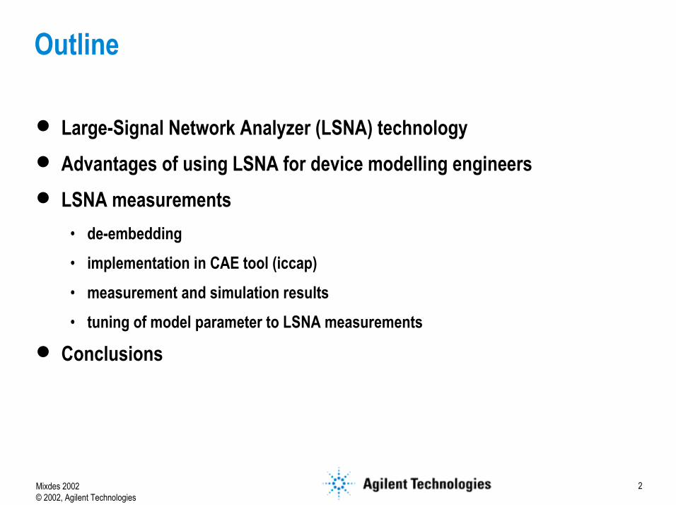
Outline
• Large-Signal Network Analyzer (LSNA) technology• Advantages of using LSNA for device modelling engineers• LSNA measurements
• de-embedding• implementation in CAE tool (iccap)• measurement and simulation results• tuning of model parameter to LSNA measurements
• Conclusions
Mixdes 2002© 2002, Agilent Technologies
3
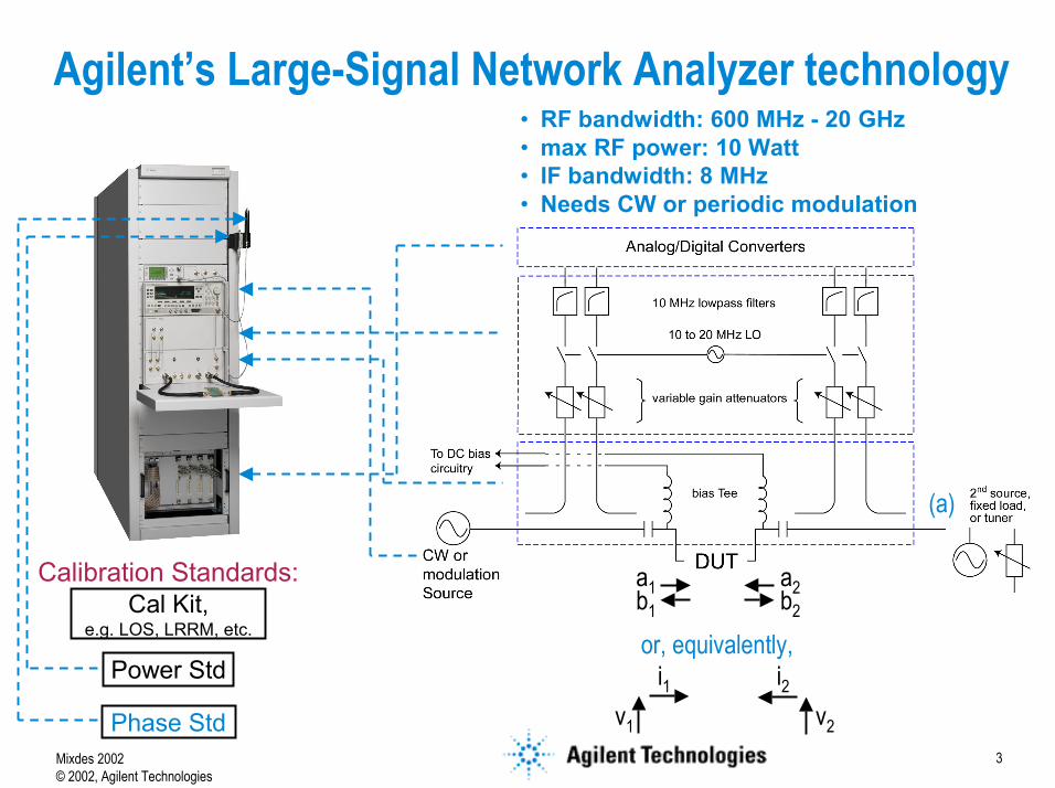
Agilent’s Large-Signal Network Analyzer technology
Cal Kit,e.g. LOS, LRRM, etc.
Power Std
Phase Std
Calibration Standards: a1b1
a2b2
i1v1
or, equivalently,i2
v2
(a)
• RF bandwidth: 600 MHz - 20 GHz• max RF power: 10 Watt• IF bandwidth: 8 MHz• Needs CW or periodic modulation
Mixdes 2002© 2002, Agilent Technologies
4
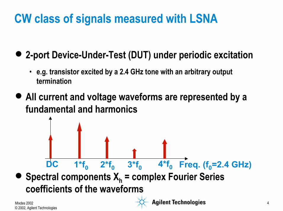
• 2-port Device-Under-Test (DUT) under periodic excitation• e.g. transistor excited by a 2.4 GHz tone with an arbitrary output
termination
• All current and voltage waveforms are represented by a fundamental and harmonics
• Spectral components Xh = complex Fourier Series coefficients of the waveforms
CW class of signals measured with LSNA
Freq. (f0=2.4 GHz)1*f0 2*f0 3*f0 4*f0DC

Mixdes 2002© 2002, Agilent Technologies
5
LSNA measurements: time domain, frequency domain or combination of both (e.g. envelope in modulation)
= ∑=
H
h
tfhjh eXtx
0
2Re)( π
∫−
−=1
0
2)(2f
tfhjh dtetxfX π
frequencylfundamentaperiodf == /1
Mixdes 2002© 2002, Agilent Technologies
6
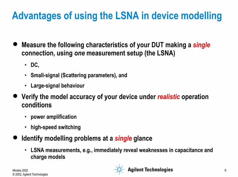
Advantages of using the LSNA in device modelling
• Measure the following characteristics of your DUT making a singleconnection, using one measurement setup (the LSNA)
• DC,• Small-signal (Scattering parameters), and• Large-signal behaviour
• Verify the model accuracy of your device under realistic operation conditions
• power amplification• high-speed switching
• Identify modelling problems at a single glance• LSNA measurements, e.g., immediately reveal weaknesses in capacitance and
charge models
Mixdes 2002© 2002, Agilent Technologies
7
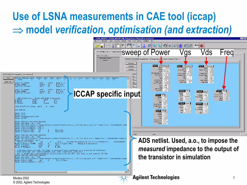
Use of LSNA measurements in CAE tool (iccap)⇒⇒⇒⇒ model verification, optimisation (and extraction)
ICCAP specific input
ADS netlist. Used, a.o., to impose themeasured impedance to the output ofthe transistor in simulation
sweep of Power Vgs Vds Freq
Mixdes 2002© 2002, Agilent Technologies
8
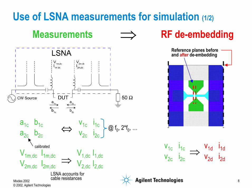
Use of LSNA measurements for simulation (1/2)
Measurements RF de-embedding
V1m,dc I1m,dcV2m,dc I2m,dc
a1c b1ca2c b2c
v1c i1cv2c i2c
calibrated
V1,dc I1,dcV2,dc I2,dc
⇒LSNA accounts forcable resistances
v1c i1cv2c i2c
v1d i1dv2d i2d
⇒
⇒
@ f0, 2*f0, …
Reference planes beforeand after de-embedding
⇔
Mixdes 2002© 2002, Agilent Technologies
9
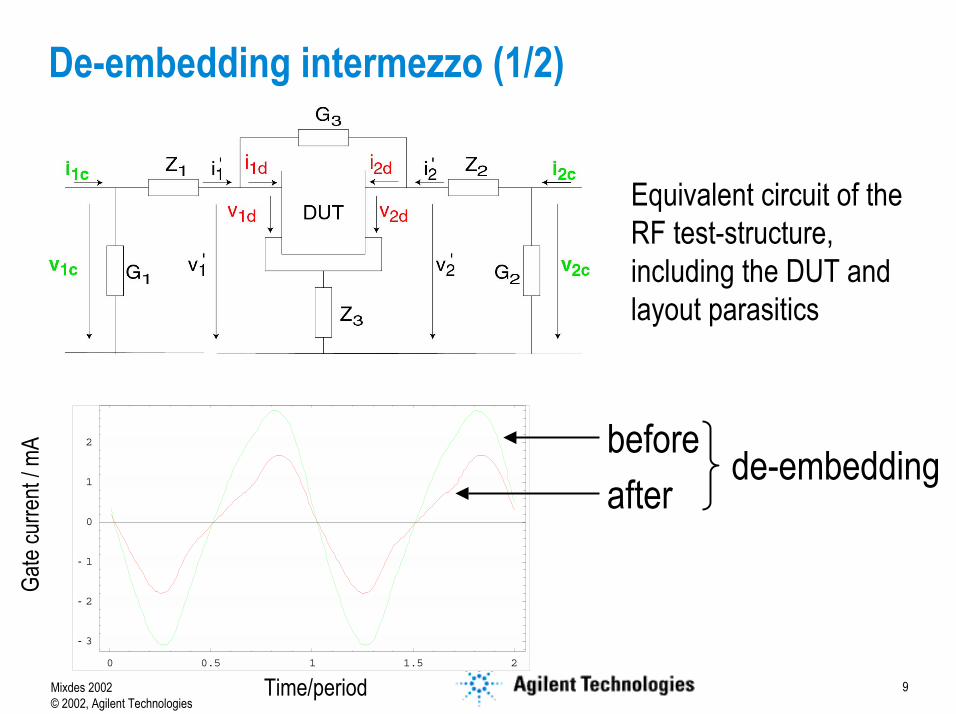
De-embedding intermezzo (1/2)
0 0.5 1 1.5 2
- 3
- 2
- 1
0
1
2 beforeafter
de-embedding
Time/period
Gate
curre
nt / m
A
Equivalent circuit of the RF test-structure, including the DUT and layout parasitics

Mixdes 2002© 2002, Agilent Technologies
10
De-embedding intermezzo (2/2)
Detailed view on the layout of the RF MOSFET
for minimum influence of pad parasitics
Mixdes 2002© 2002, Agilent Technologies
11
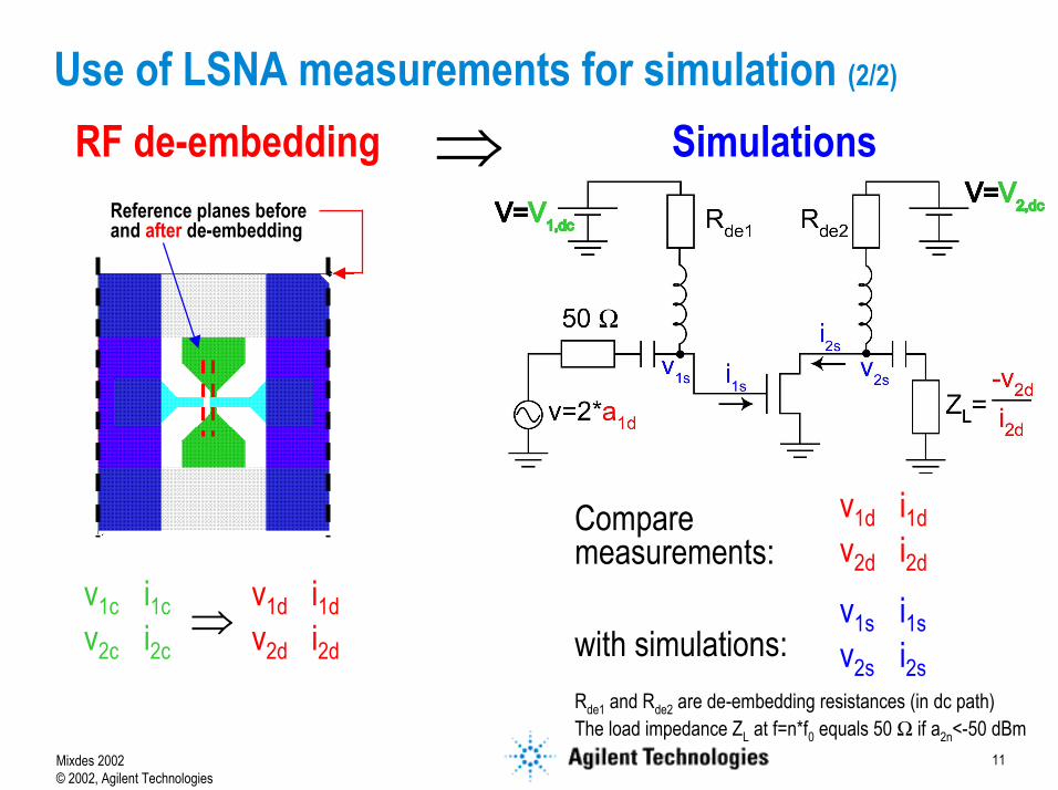
Use of LSNA measurements for simulation (2/2)
RF de-embedding Simulations
v1c i1cv2c i2c
v1d i1dv2d i2d
⇒
v1d i1dv2d i2d
Comparemeasurements:
with simulations:v1s i1sv2s i2s
⇒
Rde1 and Rde2 are de-embedding resistances (in dc path)The load impedance ZL at f=n*f0 equals 50 Ω if a2n<-50 dBm
Reference planes beforeand after de-embedding
Mixdes 2002© 2002, Agilent Technologies
12
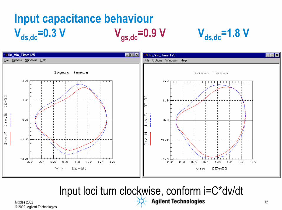
Input capacitance behaviourVgs,dc=0.9 VVds,dc=0.3 V Vds,dc=1.8 V
Input loci turn clockwise, conform i=C*dv/dt
Mixdes 2002© 2002, Agilent Technologies
13
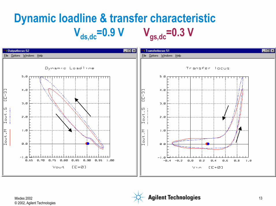
Dynamic loadline & transfer characteristicVgs,dc=0.3 VVds,dc=0.9 V
Mixdes 2002© 2002, Agilent Technologies
14
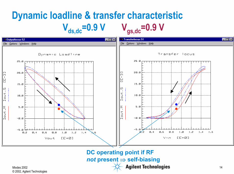
Dynamic loadline & transfer characteristicVds,dc=0.9 V Vgs,dc=0.9 V
DC operating point if RFnot present ⇒⇒⇒⇒ self-biasing
Mixdes 2002© 2002, Agilent Technologies
15
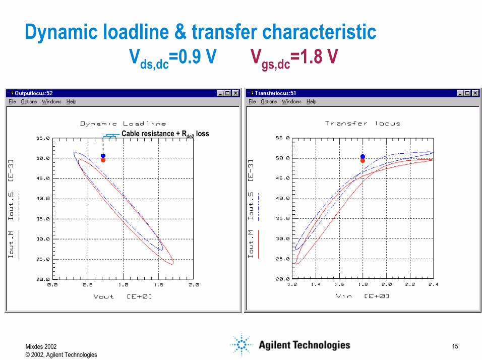
Dynamic loadline & transfer characteristicVgs,dc=1.8 V
Cable resistance + Rde2 loss
Vds,dc=0.9 V
Mixdes 2002© 2002, Agilent Technologies
16
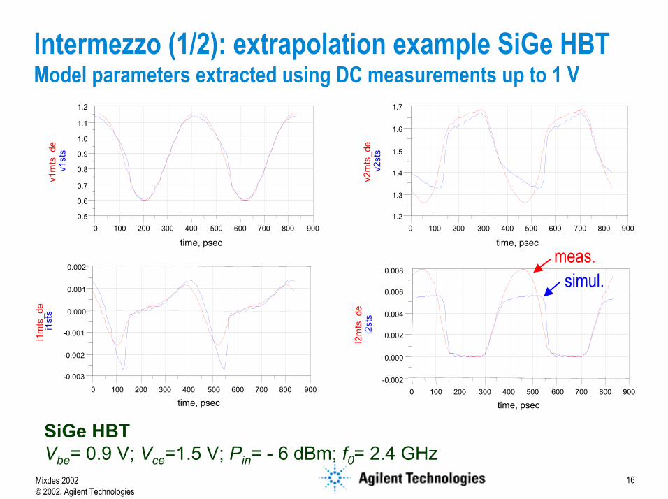
Intermezzo (1/2): extrapolation example SiGe HBTModel parameters extracted using DC measurements up to 1 V
100 200 300 400 500 600 700 8000 900
-0.002
-0.001
0.000
0.001
-0.003
0.002
time, psec
i1sts
i1mts_de
100 200 300 400 500 600 700 8000 900
0.6
0.7
0.8
0.9
1.0
1.1
0.5
1.2
time, psec
v1sts
v1mts_de
100 200 300 400 500 600 700 8000 900
1.3
1.4
1.5
1.6
1.2
1.7
time, psec
v2sts
v2mts_de
100 200 300 400 500 600 700 8000 900
0.000
0.002
0.004
0.006
-0.002
0.008
time, psec
i2sts
i2mts_de
SiGe HBT Vbe= 0.9 V; Vce=1.5 V; Pin= - 6 dBm; f0= 2.4 GHz
simul.meas.
Mixdes 2002© 2002, Agilent Technologies
17
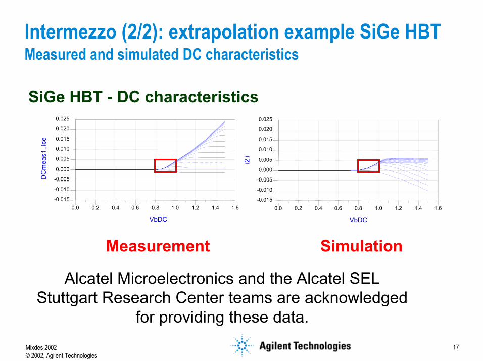
Intermezzo (2/2): extrapolation example SiGe HBTMeasured and simulated DC characteristics
Measurement Simulation
SiGe HBT - DC characteristics
0.2 0.4 0.6 0.8 1.0 1.2 1.40.0 1.6
-0.010
-0.005
0.000
0.005
0.010
0.015
0.020
-0.015
0.025
VbDC
DCmeas1..Ice
0.2 0.4 0.6 0.8 1.0 1.2 1.40.0 1.6
-0.010
-0.005
0.000
0.005
0.010
0.015
0.020
-0.015
0.025
VbDC
i2.i
Alcatel Microelectronics and the Alcatel SELStuttgart Research Center teams are acknowledged
for providing these data.
Mixdes 2002© 2002, Agilent Technologies
18
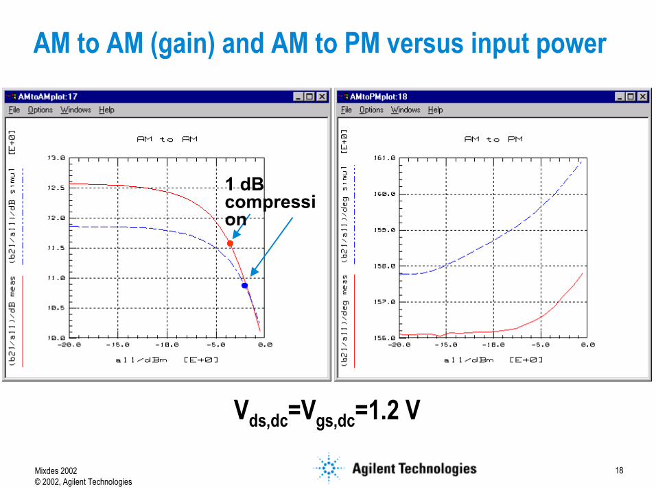
AM to AM (gain) and AM to PM versus input power
Vds,dc=Vgs,dc=1.2 V
1 dBcompression
Mixdes 2002© 2002, Agilent Technologies
19
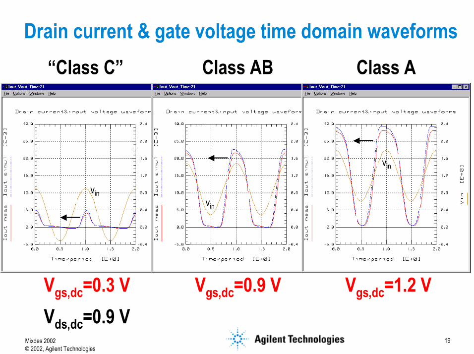
Drain current & gate voltage time domain waveforms
Vgs,dc=0.3 V
“Class C” Class AClass AB
Vgs,dc=1.2 VVgs,dc=0.9 VVds,dc=0.9 V
vinvin
vin
Mixdes 2002© 2002, Agilent Technologies
20
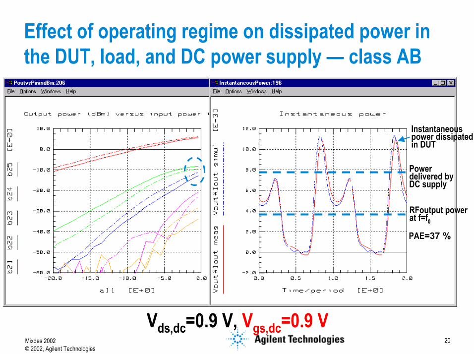
Effect of operating regime on dissipated power in the DUT, load, and DC power supply — class AB
Vds,dc=0.9 V, Vgs,dc=0.9 V
RFoutput powerat f=f0
Instantaneouspower dissipatedin DUT
Powerdelivered byDC supply
PAE=37 %
Mixdes 2002© 2002, Agilent Technologies
21
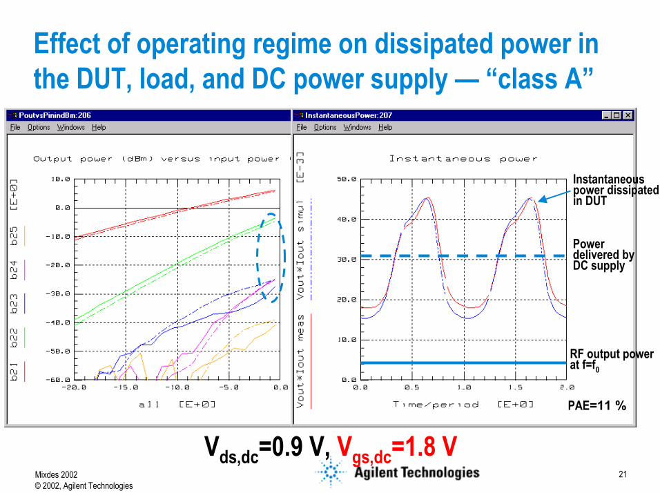
Effect of operating regime on dissipated power in the DUT, load, and DC power supply — “class A”
Vds,dc=0.9 V, Vgs,dc=1.8 V
RF output powerat f=f0
Instantaneouspower dissipatedin DUT
Powerdelivered byDC supply
PAE=11 %
Mixdes 2002© 2002, Agilent Technologies
22
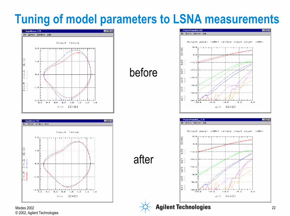
Tuning of model parameters to LSNA measurements
before
after
Mixdes 2002© 2002, Agilent Technologies
23
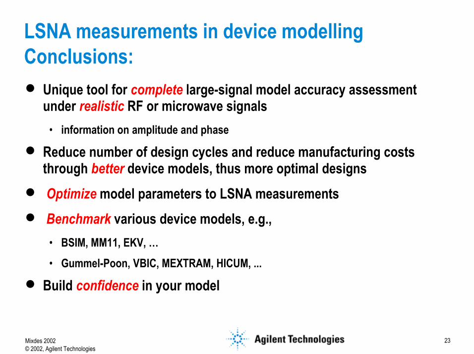
LSNA measurements in device modellingConclusions:• Unique tool for complete large-signal model accuracy assessment
under realistic RF or microwave signals• information on amplitude and phase
• Reduce number of design cycles and reduce manufacturing costs through better device models, thus more optimal designs
• Optimize model parameters to LSNA measurements• Benchmark various device models, e.g.,
• BSIM, MM11, EKV, …• Gummel-Poon, VBIC, MEXTRAM, HICUM, ...
• Build confidence in your model

Mixdes 2002© 2002, Agilent Technologies
24
Contact
• For info on LSNA technology, visithttp://www.agilent.com/find/lsna
• Soon, a measurement and consulting service related to Large-Signal Network Analyzer Technology will be available through the ‘NMDG’group in Belgium. For info, you need to contact NMDG directly atemail: [email protected], ortel.: +32 - 3 - 890 46 16