RF Power LDMOS Transistor - NXP...
28
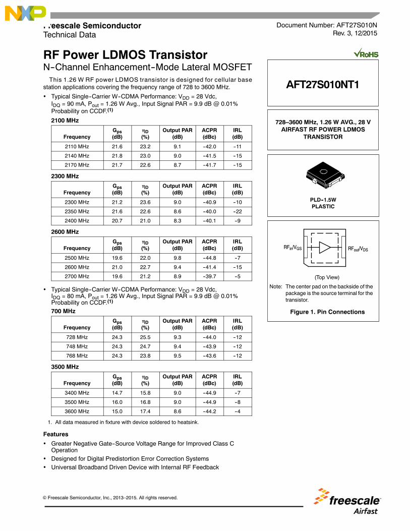
RF Power LDMOS Transistor N--Channel Enhancement--Mode Lateral MOSFET This 1.26 W RF power LDMOS transistor is designed for cellular base station applications covering the frequency range of 728 to 3600 MHz. Typical Single--Carrier W--CDMA Performance: V DD = 28 Vdc, I DQ = 90 mA, P out = 1.26 W Avg., Input Signal PAR = 9.9 dB @ 0.01% Probability on CCDF. (1) 2100 MHz Frequency G ps (dB) D (%) Output PAR (dB) ACPR (dBc) IRL (dB) 2110 MHz 21.6 23.2 9.1 --42.0 --11 2140 MHz 21.8 23.0 9.0 --41.5 --15 2170 MHz 21.7 22.6 8.7 --41.7 --15 2300 MHz Frequency G ps (dB) D (%) Output PAR (dB) ACPR (dBc) IRL (dB) 2300 MHz 21.2 23.6 9.0 --40.9 --10 2350 MHz 21.6 22.6 8.6 --40.0 --22 2400 MHz 20.7 21.0 8.3 --40.1 --9 2600 MHz Frequency G ps (dB) D (%) Output PAR (dB) ACPR (dBc) IRL (dB) 2500 MHz 19.6 22.0 9.8 --44.8 --7 2600 MHz 21.0 22.7 9.4 --41.4 --15 2700 MHz 19.6 21.2 8.9 --39.7 --5 Typical Single--Carrier W--CDMA Performance: V DD = 28 Vdc, I DQ = 80 mA, P out = 1.26 W Avg., Input Signal PAR = 9.9 dB @ 0.01% Probability on CCDF. (1) 700 MHz Frequency G ps (dB) D (%) Output PAR (dB) ACPR (dBc) IRL (dB) 728 MHz 24.3 25.5 9.3 --44.0 --12 748 MHz 24.3 24.7 9.4 --43.9 --12 768 MHz 24.3 23.8 9.5 --43.6 --12 3500 MHz Frequency G ps (dB) D (%) Output PAR (dB) ACPR (dBc) IRL (dB) 3400 MHz 14.7 15.8 9.0 --44.9 --7 3500 MHz 16.0 16.8 9.0 --44.9 --8 3600 MHz 15.0 17.4 8.6 --44.2 --4 1. All data measured in fixture with device soldered to heatsink. Features Greater Negative Gate--Source Voltage Range for Improved Class C Operation Designed for Digital Predistortion Error Correction Systems Universal Broadband Driven Device with Internal RF Feedback Document Number: AFT27S010N Rev. 3, 12/2015 Freescale Semiconductor Technical Data 728–3600 MHz, 1.26 W AVG., 28 V AIRFAST RF POWER LDMOS TRANSISTOR AFT27S010NT1 PLD--1.5W PLASTIC Figure 1. Pin Connections Note: The center pad on the backside of the package is the source terminal for the transistor. (Top View) RF out /V DS RF in /V GS Freescale Semiconductor, Inc., 2013–2015. All rights reserved.
Transcript of RF Power LDMOS Transistor - NXP...
AFT27S010NT1
1RF Device DataFreescale Semiconductor, Inc.
RF Power LDMOS TransistorN--Channel Enhancement--Mode Lateral MOSFETThis 1.26 W RF power LDMOS transistor is designed for cellular base
station applications covering the frequency range of 728 to 3600 MHz.
Typical Single--Carrier W--CDMA Performance: VDD = 28 Vdc,IDQ = 90 mA, Pout = 1.26 W Avg., Input Signal PAR = 9.9 dB @ 0.01%Probability on CCDF.(1)
2100 MHz
FrequencyGps(dB)
D(%)
Output PAR(dB)
ACPR(dBc)
IRL(dB)
2110 MHz 21.6 23.2 9.1 --42.0 --11
2140 MHz 21.8 23.0 9.0 --41.5 --15
2170 MHz 21.7 22.6 8.7 --41.7 --15
2300 MHz
FrequencyGps(dB)
D(%)
Output PAR(dB)
ACPR(dBc)
IRL(dB)
2300 MHz 21.2 23.6 9.0 --40.9 --10
2350 MHz 21.6 22.6 8.6 --40.0 --22
2400 MHz 20.7 21.0 8.3 --40.1 --9
2600 MHz
FrequencyGps(dB)
D(%)
Output PAR(dB)
ACPR(dBc)
IRL(dB)
2500 MHz 19.6 22.0 9.8 --44.8 --7
2600 MHz 21.0 22.7 9.4 --41.4 --15
2700 MHz 19.6 21.2 8.9 --39.7 --5
Typical Single--Carrier W--CDMA Performance: VDD = 28 Vdc,IDQ = 80 mA, Pout = 1.26 W Avg., Input Signal PAR = 9.9 dB @ 0.01%Probability on CCDF.(1)
700 MHz
FrequencyGps(dB)
D(%)
Output PAR(dB)
ACPR(dBc)
IRL(dB)
728 MHz 24.3 25.5 9.3 --44.0 --12
748 MHz 24.3 24.7 9.4 --43.9 --12
768 MHz 24.3 23.8 9.5 --43.6 --12
3500 MHz
FrequencyGps(dB)
D(%)
Output PAR(dB)
ACPR(dBc)
IRL(dB)
3400 MHz 14.7 15.8 9.0 --44.9 --7
3500 MHz 16.0 16.8 9.0 --44.9 --8
3600 MHz 15.0 17.4 8.6 --44.2 --4
1. All data measured in fixture with device soldered to heatsink.
Features
Greater Negative Gate--Source Voltage Range for Improved Class COperation
Designed for Digital Predistortion Error Correction Systems Universal Broadband Driven Device with Internal RF Feedback
Document Number: AFT27S010NRev. 3, 12/2015
Freescale SemiconductorTechnical Data
728–3600 MHz, 1.26 W AVG., 28 VAIRFAST RF POWER LDMOS
TRANSISTOR
AFT27S010NT1
PLD--1.5WPLASTIC
Figure 1. Pin Connections
Note: The center pad on the backside of thepackage is the source terminal for thetransistor.
(Top View)
RFout/VDSRFin/VGS
Freescale Semiconductor, Inc., 2013–2015. All rights reserved.
2RF Device Data
Freescale Semiconductor, Inc.
AFT27S010NT1
Table 1. Maximum Ratings
Rating Symbol Value Unit
Drain--Source Voltage VDSS --0.5, +65 Vdc
Gate--Source Voltage VGS --6.0, +10 Vdc
Operating Voltage VDD 32, +0 Vdc
Storage Temperature Range Tstg --65 to +150 C
Case Operating Temperature Range TC --40 to +150 C
Operating Junction Temperature Range (1,2) TJ --40 to +150 C
Table 2. Thermal Characteristics
Characteristic Symbol Value (2,3) Unit
Thermal Resistance, Junction to CaseCase Temperature 77C, 1.3 W CW, 28 Vdc, IDQ = 90 mA, 2140 MHz
RJC 3.5 C/W
Table 3. ESD Protection Characteristics
Test Methodology Class
Human Body Model (per JESD22--A114) 1B
Machine Model (per EIA/JESD22--A115) A
Charge Device Model (per JESD22--C101) III
Table 4. Moisture Sensitivity Level
Test Methodology Rating Package Peak Temperature Unit
Per JESD22--A113, IPC/JEDEC J--STD--020 3 260 C
Table 5. Electrical Characteristics (TA = 25C unless otherwise noted)
Characteristic Symbol Min Typ Max Unit
Off Characteristics
Zero Gate Voltage Drain Leakage Current(VDS = 65 Vdc, VGS = 0 Vdc)
IDSS — — 10 Adc
Zero Gate Voltage Drain Leakage Current(VDS = 28 Vdc, VGS = 0 Vdc)
IDSS — — 1 Adc
Gate--Source Leakage Current(VGS = 5 Vdc, VDS = 0 Vdc)
IGSS — — 1 Adc
On Characteristics
Gate Threshold Voltage(VDS = 10 Vdc, ID = 12.1 Adc)
VGS(th) 0.8 1.2 1.6 Vdc
Gate Quiescent Voltage(VDD = 28 Vdc, ID = 90 mAdc, Measured in Functional Test)
VGS(Q) 1.5 1.8 2.3 Vdc
Drain--Source On--Voltage(VGS = 6 Vdc, ID = 121 mAdc)
VDS(on) 0.1 0.2 0.3 Vdc
1. Continuous use at maximum temperature will affect MTTF.2. MTTF calculator available at http://www.freescale.com/rf. Select Software & Tools/Development Tools/Calculators to access MTTF
calculators by product.3. Refer to AN1955, Thermal Measurement Methodology of RF Power Amplifiers. Go to http://www.freescale.com/rf. Select
Documentation/Application Notes -- AN1955.
(continued)
AFT27S010NT1
3RF Device DataFreescale Semiconductor, Inc.
Table 5. Electrical Characteristics (TA = 25C unless otherwise noted) (continued)
Characteristic Symbol Min Typ Max Unit
Functional Tests (In Freescale Test Fixture, 50 ohm system) VDD = 28 Vdc, IDQ = 90 mA, Pout = 1.26 W Avg., f = 2170 MHz, Single--CarrierW--CDMA, IQ Magnitude Clipping, Input Signal PAR = 9.9 dB @ 0.01% Probability on CCDF. ACPR measured in 3.84 MHz ChannelBandwidth @ 5 MHz Offset.
Power Gain Gps 20.0 21.7 — dB
Drain Efficiency D 18.5 21.5 — %
Adjacent Channel Power Ratio ACPR — --40.6 --37.9 dBc
Input Return Loss IRL — --14 --9 dB
Load Mismatch (In Freescale Test Fixture, 50 ohm system) IDQ = 90 mA, f = 2140 MHz
VSWR 5:1 at 32 Vdc, 13.9 W CW Output Power(3 dB Input Overdrive from 10 W CW Rated Power)
No Device Degradation
Typical Performance (In Freescale Test Fixture, 50 ohm system) VDD = 28 Vdc, IDQ = 90 mA, 2110--2170 MHz Bandwidth
Pout @ 1 dB Compression Point, CW P1dB — 10 — W
AM/PM(Maximum value measured at the P3dB compression point acrossthe 2110--2170 MHz frequency range.)
— --12.6 —
VBW Resonance Point(IMD Seventh Order Intermodulation Inflection Point)
VBWres — 120 — MHz
Gain Flatness in 60 MHz Bandwidth @ Pout = 1.26 W Avg. GF — 0.20 — dB
Gain Variation over Temperature(--30C to +85C)
G — 0.011 — dB/C
Output Power Variation over Temperature(--30C to +85C)
P1dB — 0.004 — dB/C
Table 6. Ordering Information
Device Tape and Reel Information Package
AFT27S010NT1 T1 Suffix = 1000 Units, 16 mm Tape Width, 7--inch Reel PLD--1.5W
4RF Device Data
Freescale Semiconductor, Inc.
AFT27S010NT1
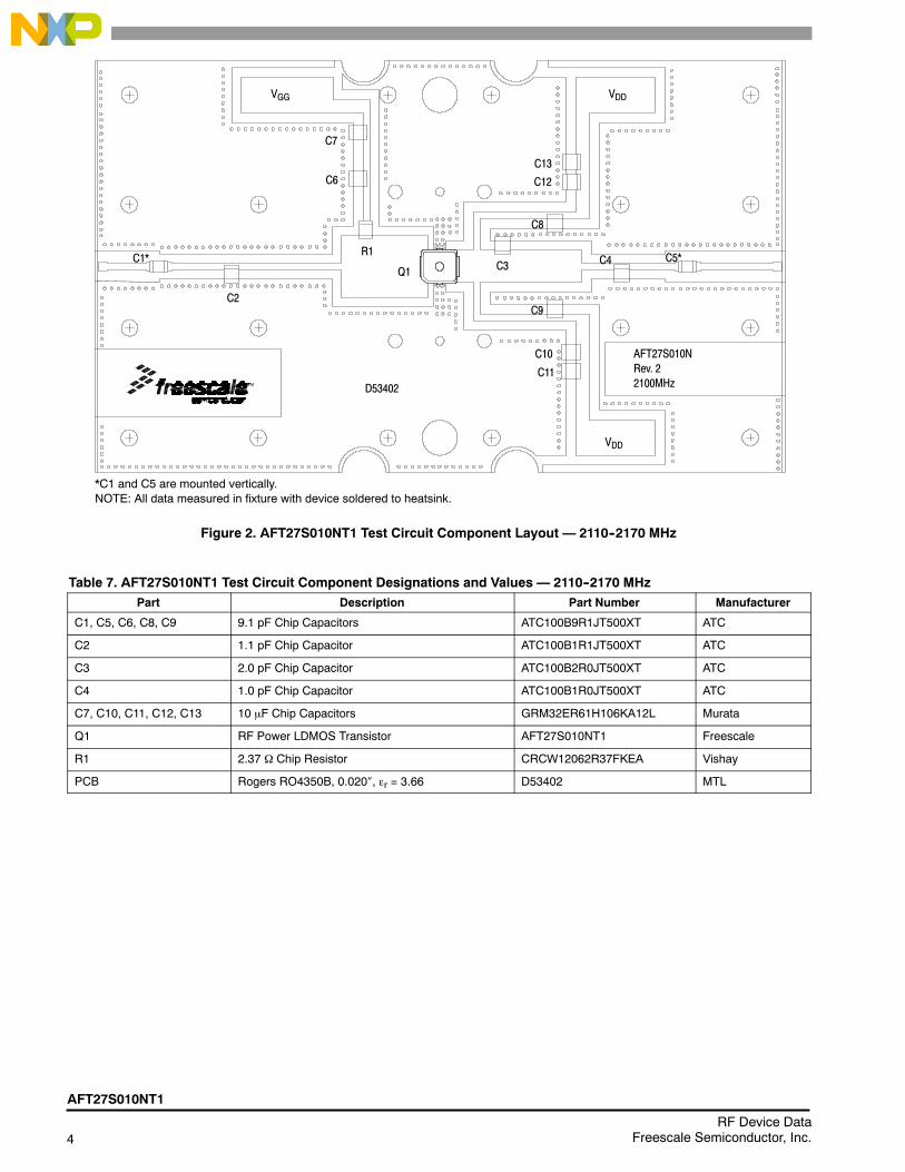
Figure 2. AFT27S010NT1 Test Circuit Component Layout — 2110--2170 MHz
C7
C6
R1
C2
C1*
C13
C12
C4 C5*C3
C8
C9
C10
C11
AFT27S010NRev. 22100MHz
*C1 and C5 are mounted vertically.NOTE: All data measured in fixture with device soldered to heatsink.
Q1
D53402
VDDVGG
VDD
Table 7. AFT27S010NT1 Test Circuit Component Designations and Values — 2110--2170 MHzPart Description Part Number Manufacturer
C1, C5, C6, C8, C9 9.1 pF Chip Capacitors ATC100B9R1JT500XT ATC
C2 1.1 pF Chip Capacitor ATC100B1R1JT500XT ATC
C3 2.0 pF Chip Capacitor ATC100B2R0JT500XT ATC
C4 1.0 pF Chip Capacitor ATC100B1R0JT500XT ATC
C7, C10, C11, C12, C13 10 F Chip Capacitors GRM32ER61H106KA12L Murata
Q1 RF Power LDMOS Transistor AFT27S010NT1 Freescale
R1 2.37 Chip Resistor CRCW12062R37FKEA Vishay
PCB Rogers RO4350B, 0.020, r = 3.66 D53402 MTL
AFT27S010NT1
5RF Device DataFreescale Semiconductor, Inc.
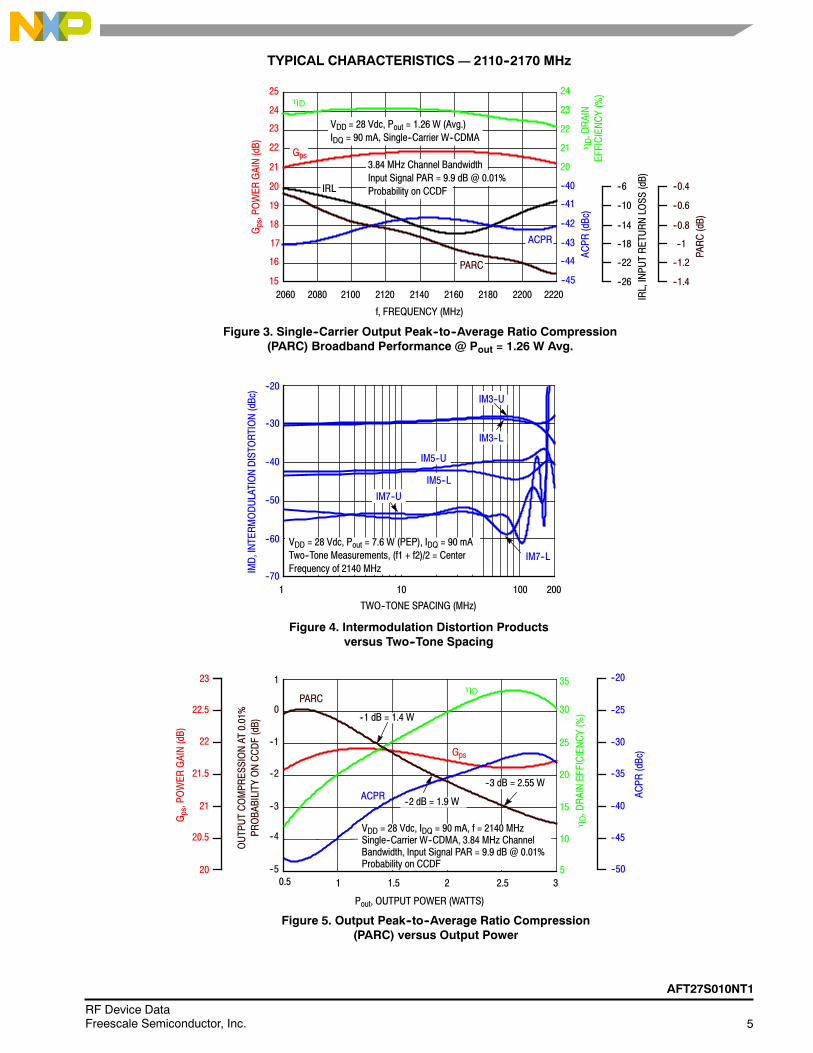
TYPICAL CHARACTERISTICS — 2110--2170 MHz
IRL,INPUTRETURNLOSS
(dB)
2060
ACPR
f, FREQUENCY (MHz)
Figure 3. Single--Carrier Output Peak--to--Average Ratio Compression(PARC) Broadband Performance @ Pout = 1.26 W Avg.
--22
--6
--10
--14
--18
16
25
24
--45
24
23
22
21
--40
--41
--42
--43
D,DRAIN
EFFICIENCY(%)
D
Gps,POWER
GAIN(dB)
23
22
21
20
19
18
17
2080 2100 2120 2140 2160 2180 2200 2220
20
--44
--26
ACPR
(dBc)
PARC
VDD = 28 Vdc, Pout = 1.26 W (Avg.)IDQ = 90 mA, Single--Carrier W--CDMA
Figure 4. Intermodulation Distortion Productsversus Two--Tone Spacing
TWO--TONE SPACING (MHz)
10--70
--20
--30
--40
--60
1 200
IMD,INTERMODULATIONDISTORTION(dBc)
--50
IM5--U
IM5--L
Figure 5. Output Peak--to--Average Ratio Compression(PARC) versus Output Power
Pout, OUTPUT POWER (WATTS)
--1
--3
1
0
--2
--4
OUTPUTCOMPRESSIONAT
0.01%
PROBABILITY
ONCCDF(dB)
0.5 1.5 2.55
35
30
25
20
15
10
DDRAINEFFICIENCY(%)
--3 dB = 2.55 W
2
D
ACPR
PARC
ACPR
(dBc)
--50
--20
--25
--30
--40
--35
--45
23
Gps,POWER
GAIN(dB)
22.5
22
21.5
21
20.5
20
--1 dB = 1.4 W
--2 dB = 1.9 W
IRL
PARC(dB)
--1.2
--0.4
--0.6
--0.8
--1
--1.4
--5
3.84 MHz Channel BandwidthInput Signal PAR = 9.9 dB @ 0.01%Probability on CCDF
1
VDD = 28 Vdc, IDQ = 90 mA, f = 2140 MHzSingle--Carrier W--CDMA, 3.84 MHz ChannelBandwidth, Input Signal PAR = 9.9 dB @ 0.01%Probability on CCDF
VDD = 28 Vdc, Pout = 7.6 W (PEP), IDQ = 90 mATwo--Tone Measurements, (f1 + f2)/2 = CenterFrequency of 2140 MHz
IM3--U
IM3--L
IM7--U
100
Gps
3
IM7--L
15
Gps
6RF Device Data
Freescale Semiconductor, Inc.
AFT27S010NT1
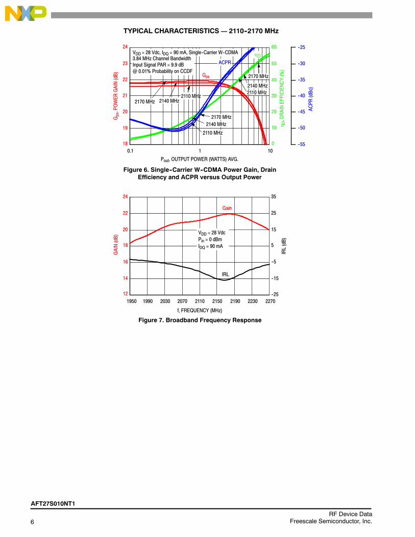
TYPICAL CHARACTERISTICS — 2110--2170 MHz
0.1
ACPR
Pout, OUTPUT POWER (WATTS) AVG.
Figure 6. Single--Carrier W--CDMA Power Gain, DrainEfficiency and ACPR versus Output Power
--30
--35
18
24
0
60
50
40
30
20
D,DRAINEFFICIENCY(%)
Gps,POWER
GAIN(dB)
23
22
1 10
10
--55
ACPR
(dBc)
21
20
19
--25
--40
--45
--50
Figure 7. Broadband Frequency Response
12
24
f, FREQUENCY (MHz)
VDD = 28 VdcPin = 0 dBmIDQ = 90 mA
20
18
16
GAIN(dB)
22
14
1950 1990 2030 2070 2110 2150 2190 2230 2270--25
35
25
15
5
--5
IRL(dB)
--15
Gain
IRL
2110 MHz
2170 MHz
2140 MHz
VDD = 28 Vdc, IDQ = 90 mA, Single--Carrier W--CDMA3.84 MHz Channel BandwidthInput Signal PAR = 9.9 dB@ 0.01% Probability on CCDF
Gps
2170 MHz
2110 MHz
2140 MHz
D
2170 MHz
2140 MHz2110 MHz
AFT27S010NT1
7RF Device DataFreescale Semiconductor, Inc.
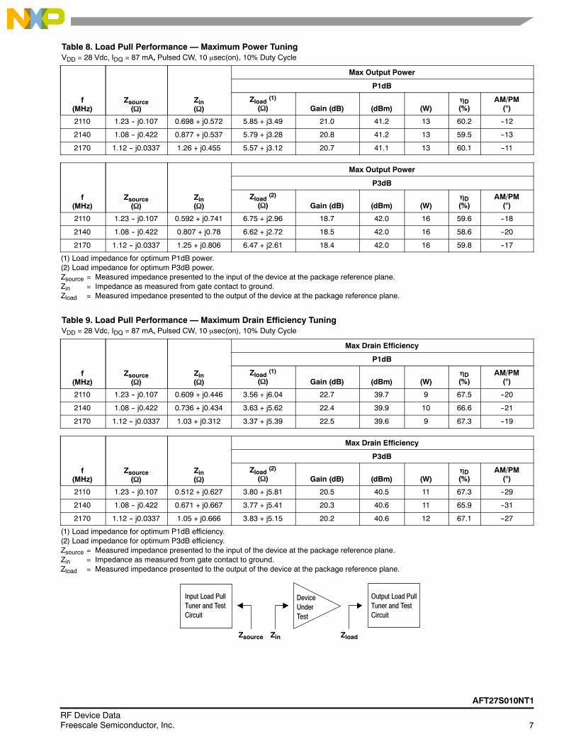
Table 8. Load Pull Performance — Maximum Power TuningVDD = 28 Vdc, IDQ = 87 mA, Pulsed CW, 10 sec(on), 10% Duty Cycle
f(MHz)
Zsource()
Zin()
Max Output Power
P1dB
Zload (1)
() Gain (dB) (dBm) (W)D(%)
AM/PM()
2110 1.23 -- j0.107 0.698 + j0.572 5.85 + j3.49 21.0 41.2 13 60.2 --12
2140 1.08 -- j0.422 0.877 + j0.537 5.79 + j3.28 20.8 41.2 13 59.5 --13
2170 1.12 -- j0.0337 1.26 + j0.455 5.57 + j3.12 20.7 41.1 13 60.1 --11
f(MHz)
Zsource()
Zin()
Max Output Power
P3dB
Zload (2)
() Gain (dB) (dBm) (W)D(%)
AM/PM()
2110 1.23 -- j0.107 0.592 + j0.741 6.75 + j2.96 18.7 42.0 16 59.6 --18
2140 1.08 -- j0.422 0.807 + j0.78 6.62 + j2.72 18.5 42.0 16 58.6 --20
2170 1.12 -- j0.0337 1.25 + j0.806 6.47 + j2.61 18.4 42.0 16 59.8 --17
(1) Load impedance for optimum P1dB power.(2) Load impedance for optimum P3dB power.Zsource = Measured impedance presented to the input of the device at the package reference plane.Zin = Impedance as measured from gate contact to ground.Zload = Measured impedance presented to the output of the device at the package reference plane.
Table 9. Load Pull Performance — Maximum Drain Efficiency TuningVDD = 28 Vdc, IDQ = 87 mA, Pulsed CW, 10 sec(on), 10% Duty Cycle
f(MHz)
Zsource()
Zin()
Max Drain Efficiency
P1dB
Zload (1)
() Gain (dB) (dBm) (W)D(%)
AM/PM()
2110 1.23 -- j0.107 0.609 + j0.446 3.56 + j6.04 22.7 39.7 9 67.5 --20
2140 1.08 -- j0.422 0.736 + j0.434 3.63 + j5.62 22.4 39.9 10 66.6 --21
2170 1.12 -- j0.0337 1.03 + j0.312 3.37 + j5.39 22.5 39.6 9 67.3 --19
f(MHz)
Zsource()
Zin()
Max Drain Efficiency
P3dB
Zload (2)
() Gain (dB) (dBm) (W)D(%)
AM/PM()
2110 1.23 -- j0.107 0.512 + j0.627 3.80 + j5.81 20.5 40.5 11 67.3 --29
2140 1.08 -- j0.422 0.671 + j0.667 3.77 + j5.41 20.3 40.6 11 65.9 --31
2170 1.12 -- j0.0337 1.05 + j0.666 3.83 + j5.15 20.2 40.6 12 67.1 --27
(1) Load impedance for optimum P1dB efficiency.(2) Load impedance for optimum P3dB efficiency.Zsource = Measured impedance presented to the input of the device at the package reference plane.Zin = Impedance as measured from gate contact to ground.Zload = Measured impedance presented to the output of the device at the package reference plane.
Input Load PullTuner and TestCircuit
DeviceUnderTest
Zsource Zin Zload
Output Load PullTuner and TestCircuit
8RF Device Data
Freescale Semiconductor, Inc.
AFT27S010NT1
P1dB -- TYPICAL LOAD PULL CONTOURS — 2140 MHz
0
8
6
IMAGINARY()
4 52 10
7
5
4
9
3
3
2
1
7 860
8
6IMAGINARY()
4 52 10
7
5
4
9
3
3
2
1
7 86
0
8
6
IMAGINARY()
4 52 10
7
5
4
9
3
3
2
1
7 86
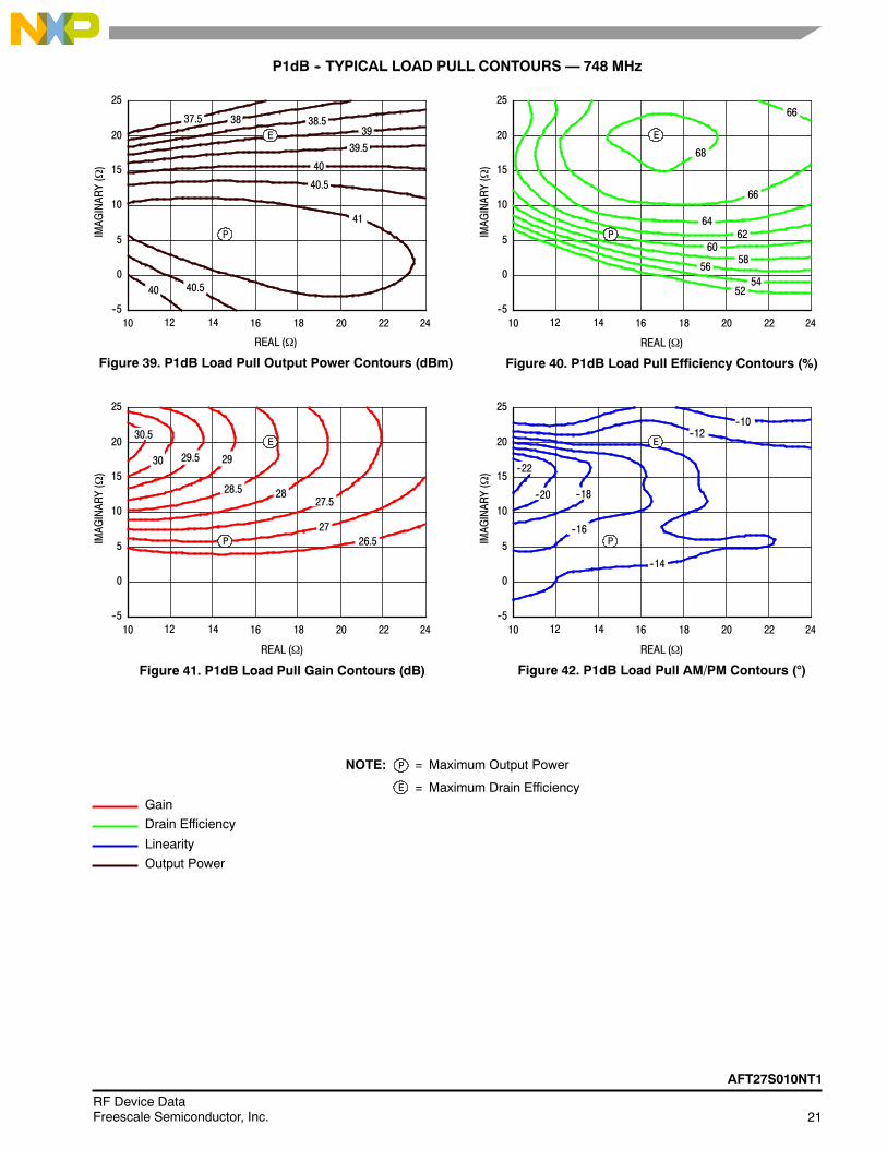
NOTE: = Maximum Output Power
= Maximum Drain Efficiency
P
E
Gain
Drain Efficiency
Linearity
Output Power
Figure 8. P1dB Load Pull Output Power Contours (dBm)
REAL ()
0
8
6
IMAGINARY()
4 52 10
7
5
4
9
3
3
Figure 9. P1dB Load Pull Efficiency Contours (%)
REAL ()
Figure 10. P1dB Load Pull Gain Contours (dB)
REAL ()
Figure 11. P1dB Load Pull AM/PM Contours ()
REAL ()
2
1
7 86
P
E
39
38
4038.5
38
37.5 39.5
40.5
41
39
39.5
60
58
56
54 52
50
62
P
E
64
66
52
P
E
21.5
20
20.5
21
20.5
22
22.5
23.5
23
P
E
--26
--24
--22
--20
--18
--16
--14
--12
--28
19.5
AFT27S010NT1
9RF Device DataFreescale Semiconductor, Inc.
P3dB -- TYPICAL LOAD PULL CONTOURS — 2140 MHz
0
8
6
IMAGINARY()
4 52 10
7
5
4
9
3
3
2
1
7 860
8
6
IMAGINARY()
4 52 10
7
5
4
9
3
3
2
1
7 86
0
8
6
IMAGINARY()
4 52 10
7
5
4
9
3
3
2
1
7 86
NOTE: = Maximum Output Power
= Maximum Drain Efficiency
P
E
Gain
Drain Efficiency
Linearity
Output Power
Figure 12. P3dB Load Pull Output Power Contours (dBm)
REAL ()
0
8
6
IMAGINARY()
4 52 10
7
5
4
9
3
3
Figure 13. P3dB Load Pull Efficiency Contours (%)
REAL ()
Figure 14. P3dB Load Pull Gain Contours (dB)
REAL ()
Figure 15. P3dB Load Pull AM/PM Contours ()
REAL ()
2
1
7 86
39.5
P
E
38
38.5
39 40
40.5 41
41.5
P
E 60
58
56
54
50
6264
52
P
E
19.5
20
19
18.5
18
17.5
20.521
21.5
P
E
--26
--24 --22
--20
--28
--30
--32
--34
54
10RF Device Data
Freescale Semiconductor, Inc.
AFT27S010NT1
2500--2700 MHz
Figure 16. AFT27S010NT1 Test Circuit Component Layout — 2500--2700 MHz
NOTE: All data measured in fixture with device soldered to heatsink.
AFT27S010NRev. 22300MHz/2500MHzD53817
VDDVGG
VDD
C6
C5
R1
C2
C1
C12
C11
C4C3
C7
C8
C9
C10
Q1
C13
Table 10. AFT27S010NT1 Test Circuit Component Designations and Values — 2500--2700 MHzPart Description Part Number Manufacturer
C1, C4, C5, C7, C8 6.8 pF Chip Capacitors ATC100B6R8JT500XT ATC
C2 1.2 pF Chip Capacitor ATC100B1R2JT500XT ATC
C3 1 pF Chip Capacitor ATC100B1R0JT500XT ATC
C6, C9, C10, C11, C12 10 F Chip Capacitors GRM32ER61H106KA12L Murata
C13 220 F, 50 V Electrolytic Capacitor 227CKS050M Illinois Capacitor
Q1 RF Power LDMOS Transistor AFT27S010NT1 Freescale
R1 4.75 Chip Resistor CRCW12064R75FKEA Vishay
PCB Rogers RO4350B, 0.020, r = 3.66 D53817 MTL
AFT27S010NT1
11RF Device DataFreescale Semiconductor, Inc.
TYPICAL CHARACTERISTICS — 2500--2700 MHz
--44
--42
--40
--38
--36
19
Pout, OUTPUT POWER (WATTS) AVG.
--20
--30
D,DRAINEFFICIENCY(%)
Gps,POWER
GAIN(dB)
--70
ACPR
(dBc)
--10
--40
--50
--60
0
30
f, FREQUENCY (MHz)
20
15
10
GAIN(dB)
25
5
2300 2400 2500 2600 2700 2800 2900
IRL(dB)
IRL,INPUTRETURNLOSS
(dB)
2480
ACPR
f, FREQUENCY (MHz)
Figure 17. Single--Carrier Output Peak--to--Average Ratio Compression(PARC) Broadband Performance @ Pout = 1.26 W Avg.
--20
0
--5
--10
--15
18.5
23.5
23
22.5
--46
24
23
22
21 D,DRAIN
EFFICIENCY(%)
D
Gps,POWER
GAIN(dB) 22
21.5
21
20.5
20
19.5
2510 2540 2570 2600 2630 2660 2690 2720
20
--25
ACPR
(dBc)PARC
IRL
PARC(dB)
--2
0
--0.5
--1
--1.5
--2.5
Gps
Figure 18. Single--Carrier W--CDMA Power Gain, DrainEfficiency and ACPR versus Output Power
Figure 19. Broadband Frequency Response
0.312
24
5
65
55
35
25
22
10
18
16
2500 MHz
Gain
IRL
VDD = 28 VdcPin = 0 dBmIDQ = 90 mA
1
Gps
D2600 MHz
20
2600 MHz
2500 MHz
2600 MHz
10
5
0
--5
--10
--15
--20
20
14
45
152700 MHz2500 MHz
2700 MHz2700 MHz
VDD = 28 Vdc, IDQ = 90 mA, Single--Carrier, W--CDMA3.84 MHz Channel Bandwidth, Input Signal = 9.9 dB @0.01% Probability on CCDF
ACPR
Input Signal PAR = 9.9 dB @ 0.01%Probability on CCDF
VDD = 28 Vdc, Pout = 1.26 W (Avg.)IDQ = 90 mA, Single--Carrier W--CDMA3.84 MHz Channel Bandwidth
12RF Device Data
Freescale Semiconductor, Inc.
AFT27S010NT1
2300--2400 MHz
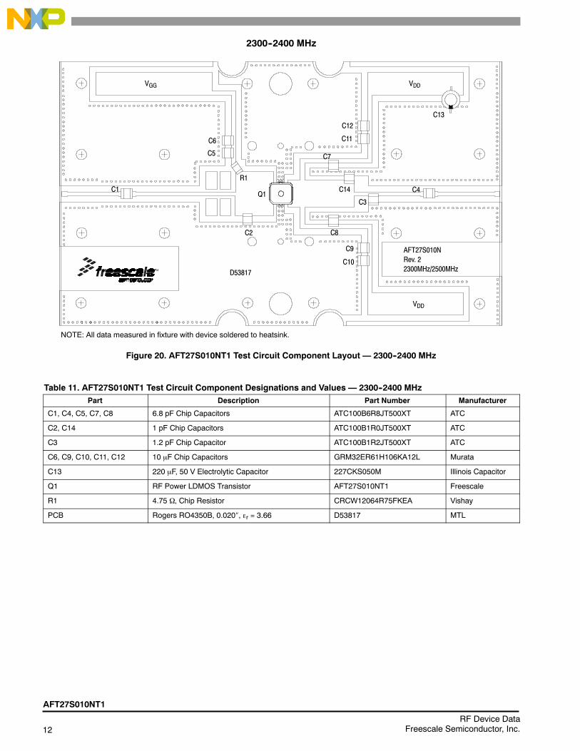
Figure 20. AFT27S010NT1 Test Circuit Component Layout — 2300--2400 MHz
NOTE: All data measured in fixture with device soldered to heatsink.
AFT27S010NRev. 22300MHz/2500MHzD53817
VDDVGG
VDD
C6
C5
R1
C2
C1
C12
C11
C4
C3
C7
C8
C9
C10
Q1C14
C13
Table 11. AFT27S010NT1 Test Circuit Component Designations and Values — 2300--2400 MHzPart Description Part Number Manufacturer
C1, C4, C5, C7, C8 6.8 pF Chip Capacitors ATC100B6R8JT500XT ATC
C2, C14 1 pF Chip Capacitors ATC100B1R0JT500XT ATC
C3 1.2 pF Chip Capacitor ATC100B1R2JT500XT ATC
C6, C9, C10, C11, C12 10 F Chip Capacitors GRM32ER61H106KA12L Murata
C13 220 F, 50 V Electrolytic Capacitor 227CKS050M Illinois Capacitor
Q1 RF Power LDMOS Transistor AFT27S010NT1 Freescale
R1 4.75 , Chip Resistor CRCW12064R75FKEA Vishay
PCB Rogers RO4350B, 0.020, r = 3.66 D53817 MTL
AFT27S010NT1
13RF Device DataFreescale Semiconductor, Inc.
TYPICAL CHARACTERISTICS — 2300--2400 MHz
Pout, OUTPUT POWER (WATTS) AVG.
0
--10
D,DRAINEFFICIENCY(%)
Gps,POWER
GAIN(dB)
--50
ACPR
(dBc)
10
--20
--30
--40
0
30
f, FREQUENCY (MHz)
20
15
10
GAIN(dB)
25
5
2050 2150 2250 2350 2450 2550 2650--25
5
0
--5
--10
--15
IRL(dB)
--20
IRL,INPUTRETURNLOSS
(dB)
2290
f, FREQUENCY (MHz)
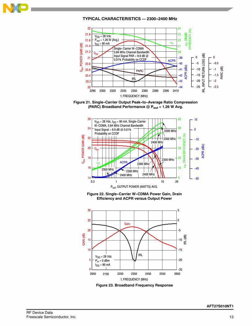
Figure 21. Single--Carrier Output Peak--to--Average Ratio Compression(PARC) Broadband Performance @ Pout = 1.26 W Avg.
--20
0
--5
--10
--15
20
22
21.8
21.6
--44
24
23
22
21
--39
--40
--41
--42
D,DRAIN
EFFICIENCY(%)
D
Gps,POWER
GAIN(dB) 21.4
21.2
21
20.8
20.6
20.4
20.2
2305 2320 2335 2350 2365 2380 2395 2410
20
--43
--25
ACPR
(dBc)
PARC
IRL PARC(dB)
--2
0
--0.5
--1
--1.5
--2.5
Gps
Figure 22. Single--Carrier W--CDMA Power Gain, DrainEfficiency and ACPR versus Output Power
Figure 23. Broadband Frequency Response
0.314
26
0
60
50
4022
20
10
30
18
Gain
IRLVDD = 28 VdcPin = 0 dBmIDQ = 90 mA
1
VDD = 28 VdcPout = 1.26 W (Avg.)IDQ = 90 mA
20
VDD = 28 Vdc, IDQ = 90 mA, Single--CarrierW--CDMA, 3.84 MHz Channel BandwidthInput Signal = 9.9 dB @ 0.01%Probability on CCDF
Single--Carrier W--CDMA3.84 MHz Channel BandwidthInput Signal PAR = 9.9 dB @0.01% Probability on CCDF ACPR
24
16
20
102300 MHz2350 MHz
2400 MHz 2400 MHz
2300 MHz2350 MHz
2400 MHz2350 MHz
2300 MHz
Gps
D ACPR
14RF Device Data
Freescale Semiconductor, Inc.
AFT27S010NT1
Table 12. Load Pull Performance — Maximum Power TuningVDD = 28 Vdc, IDQ = 87 mA, Pulsed CW, 10 sec(on), 10% Duty Cycle
f(MHz)
Zsource()
Zin()
Max Output Power
P1dB
Zload (1)
() Gain (dB) (dBm) (W)D(%)
AM/PM()
2300 1.12 -- j1.10 0.995 + j1.38 5.39 + j2.23 20.1 40.9 12 55.9 --12
2400 1.06 -- j1.59 0.948 + j1.96 5.09 + j1.86 19.8 40.9 12 55.1 --12
2500 1.00 -- j1.60 1.29 + j1.95 4.51 + j1.56 19.2 40.8 12 55.8 --10
2600 0.985 -- j3.50 0.743 + j3.66 4.81 + j1.10 19.0 41.3 13 56.2 --14
2690 1.10 -- j3.13 1.48 + j2.98 4.14 + j0.987 19.0 41.0 13 57.5 --12
f(MHz)
Zsource()
Zin()
Max Output Power
P3dB
Zload (2)
() Gain (dB) (dBm) (W)D(%)
AM/PM()
2300 1.12 -- j1.10 0.919 + j1.64 6.28 + j1.74 17.8 41.7 15 55.0 --19
2400 1.06 -- j1.59 0.861 + j2.23 5.86 + j1.41 17.5 41.7 15 54.4 --19
2500 1.00 -- j1.60 1.37 + j2.32 5.40 + j1.17 16.9 41.7 15 55.8 --17
2600 0.985 -- j3.50 0.579 + j3.82 5.37 + j0.912 16.9 42.0 16 55.8 --22
2690 1.10 -- j3.13 1.74 + j3.43 5.04 + j0.759 16.8 41.8 15 57.1 --18
(1) Load impedance for optimum P1dB power. (2) Load impedance for optimum P3dB power.Zsource = Measured impedance presented to the input of the device at the package reference plane.Zin = Impedance as measured from gate contact to ground.Zload = Measured impedance presented to the output of the device at the package reference plane.
Table 13. Load Pull Performance — Maximum Drain Efficiency TuningVDD = 28 Vdc, IDQ = 87 mA, Pulsed CW, 10 sec(on), 10% Duty Cycle
f(MHz)
Zsource()
Zin()
Max Drain Efficiency
P1dB
Zload (1)
() Gain (dB) (dBm) (W)D(%)
AM/PM()
2300 1.12 -- j1.10 0.855 + j1.22 3.36 + j4.23 21.6 39.8 9 61.9 --20
2400 1.06 -- j1.59 0.829 + j1.80 3.34 + j3.53 21.2 39.9 10 60.4 --19
2500 1.00 -- j1.60 1.04 + j1.82 3.21 + j3.00 20.8 40.0 10 61.1 --16
2600 0.985 -- j3.50 0.709 + j3.49 3.17 + j2.53 20.0 40.5 11 60.7 --20
2690 1.10 -- j3.13 1.14 + j2.91 2.87 + j2.16 20.4 40.2 10 62.0 --18
f(MHz)
Zsource()
Zin()
Max Drain Efficiency
P3dB
Zload (2)
() Gain (dB) (dBm) (W)D(%)
AM/PM()
2300 1.12 j1.10 0.803 + j1.51 3.96 + j4.10 19.4 40.7 12 61.1 --27
2400 1.06 -- j1.59 0.757 + j2.07 3.70 + j3.45 19.1 40.6 12 59.8 --27
2500 1.00 -- j1.60 1.15 + j2.18 3.58 + j2.94 18.7 40.8 12 61.2 --24
2600 0.985 -- j3.50 0.556 + j3.73 4.15 + j2.29 17.8 41.5 14 59.7 --26
2690 1.10 -- j3.13 1.43 + j3.33 3.40 + j2.01 18.2 41.1 13 61.7 --25
(1) Load impedance for optimum P1dB efficiency. (2) Load impedance for optimum P3dB efficiency.Zsource = Measured impedance presented to the input of the device at the package reference plane.Zin = Impedance as measured from gate contact to ground.Zload = Measured impedance presented to the output of the device at the package reference plane.
Input Load PullTuner and TestCircuit
DeviceUnderTest
Zsource Zin Zload
Output Load PullTuner and TestCircuit
AFT27S010NT1
15RF Device DataFreescale Semiconductor, Inc.
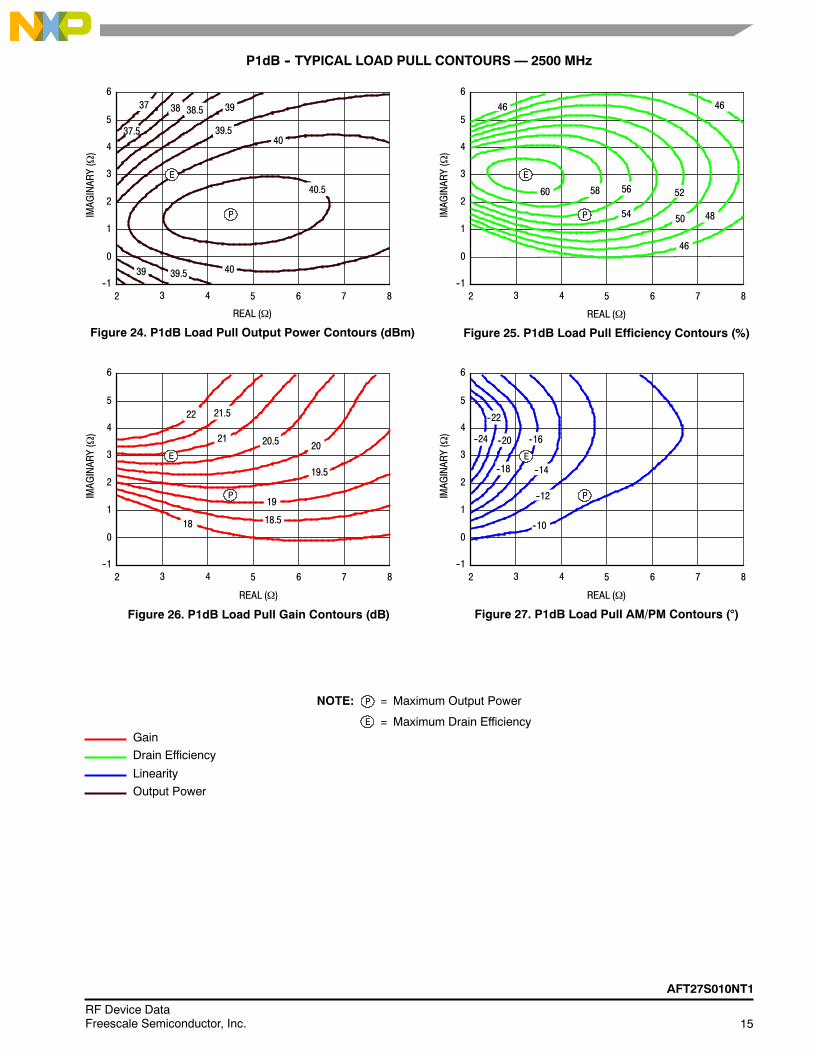
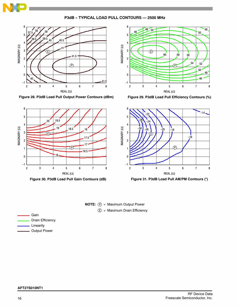
P1dB -- TYPICAL LOAD PULL CONTOURS — 2500 MHz
--1
6
4
4 5 62 8
5
3
2
7
1
3
0
--1
6
4
4 5 62 8
5
3
2
7
1
3
0
--1
6
4
4 5 62 8
5
3
2
7
1
3
0
IMAGINARY()
NOTE: = Maximum Output Power
= Maximum Drain Efficiency
P
E
Gain
Drain Efficiency
Linearity
Output Power
Figure 24. P1dB Load Pull Output Power Contours (dBm)
REAL ()
--1
6
4
IMAGINARY()
4 5 62 8
5
3
2
7
1
3
Figure 25. P1dB Load Pull Efficiency Contours (%)
REAL ()
Figure 26. P1dB Load Pull Gain Contours (dB)
REAL ()
Figure 27. P1dB Load Pull AM/PM Contours ()
REAL ()
0
IMAGINARY()
IMAGINARY()
P
E
37
37.5
38 38.5 39
39.540
40.5
39 39.5 40
P
E
60 58 56
54
52
50 48
46
46 46
19.5
20
19
18.518
P
E
20.521
21.522
P
E
--16
--12
--10
--18
--20
--22
--24
--14
16RF Device Data
Freescale Semiconductor, Inc.
AFT27S010NT1
P3dB -- TYPICAL LOAD PULL CONTOURS — 2500 MHz
--1
6
4
4 5 62 8
5
3
2
7
1
3
0
--1
6
4
4 5 62 8
5
3
2
7
1
3
0
--1
6
4
4 5 62 8
5
3
2
7
1
3
0
IMAGINARY()
NOTE: = Maximum Output Power
= Maximum Drain Efficiency
P
E
Gain
Drain Efficiency
Linearity
Output Power
Figure 28. P3dB Load Pull Output Power Contours (dBm)
REAL ()
--1
6
4
IMAGINARY()
4 5 62 8
5
3
2
7
1
3
Figure 29. P3dB Load Pull Efficiency Contours (%)
REAL ()
Figure 30. P3dB Load Pull Gain Contours (dB)
REAL ()
Figure 31. P3dB Load Pull AM/PM Contours ()
REAL ()
0
IMAGINARY()
IMAGINARY()
P
E
37.5
4041
38
38.5
39
39.5 40 40.5
41
41.5
P
E
48
54 52
504846 50
46
4850
565860
P
E
19.520
19 18.5
17.5
17
16.516
18
P
E
--26
--24
--22
--20 --18
--16
--14
--28
--30
AFT27S010NT1
17RF Device DataFreescale Semiconductor, Inc.
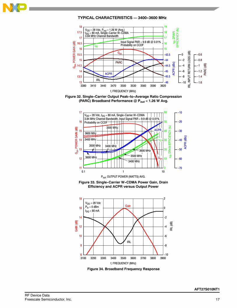
TYPICAL CHARACTERISTICS — 3400--3600 MHz
--1.4
--0.6
--0.8
--1
--1.2
--1.6
IRL,INPUTRETURNLOSS
(dB)
--8
0
--2
--4
--6
--10
PARC(dB)
3380
f, FREQUENCY (MHz)
Figure 32. Single--Carrier Output Peak--to--Average Ratio Compression(PARC) Broadband Performance @ Pout = 1.26 W Avg.
13
18
17.5
17
--46
19
18
17
16
--43.5
--44
--44.5
--45
D,DRAIN
EFFICIENCY(%)
Gps,POWER
GAIN(dB) 16.5
16
15.5
15
14.5
14
13.5
3410 3440 3470 3500 3530 3560 3590 3620
15
--45.5
ACPR
(dBc)
ACPR
D
PARC
Gps
IRL
Input Signal PAR = 9.9 dB @ 0.01%Probability on CCDF
0.1
Pout, OUTPUT POWER (WATTS) AVG.
Figure 33. Single--Carrier W--CDMA Power Gain, DrainEfficiency and ACPR versus Output Power
--20
--30
11
17
0
60
50
40
30
20
D,DRAINEFFICIENCY(%)
Gps,POWER
GAIN(dB)
16
15
1 10
10
--70
ACPR
(dBc)
14
13
12
--10
--40
--50
--60
3500 MHz
3400 MHz
3600 MHzACPR
3600 MHz
3500 MHz 3400 MHz
3400 MHz
3500 MHz
3600 MHz
D
Figure 34. Broadband Frequency Response
6
18
f, FREQUENCY (MHz)
14
12
10
GAIN(dB)
16
8
3100 3200 3300 3400 3500 3600 3700 3800 3900
GainVDD = 28 VdcPin = 0 dBmIDQ = 80 mA
--10
2
0
--2
--4
--6
IRL(dB)
--8IRL
Gps
VDD = 28 Vdc, IDQ = 80 mA, Single--Carrier W--CDMA3.84 MHz Channel Bandwidth, Input Signal PAR = 9.9 dB @ 0.01%Probability on CCDF
VDD = 28 Vdc, Pout = 1.26 W (Avg.)IDQ = 80 mA, Single--Carrier W--CDMA3.84 MHz Channel Bandwidth
18RF Device Data
Freescale Semiconductor, Inc.
AFT27S010NT1
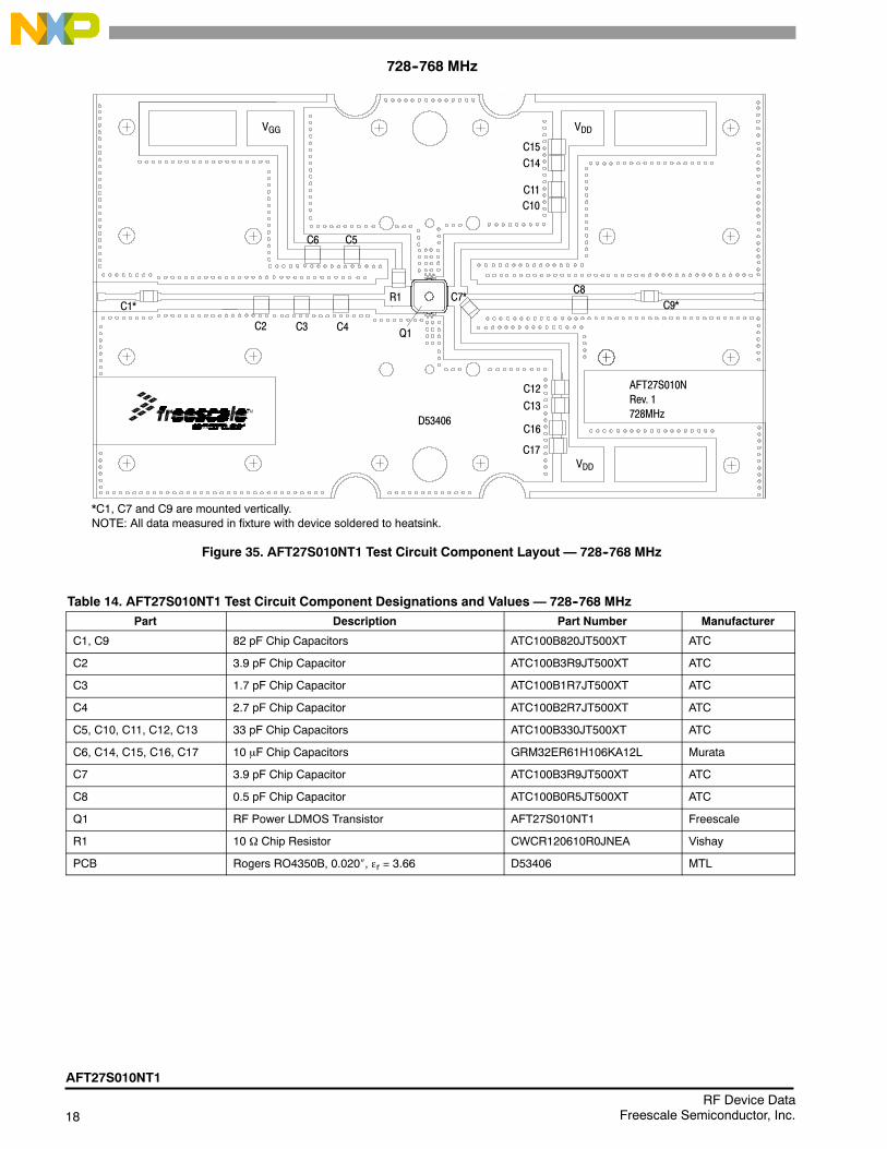
728--768 MHz
Figure 35. AFT27S010NT1 Test Circuit Component Layout — 728--768 MHz
C15C14
C11C10
C5C6
C3
C17
C16
C13
C12
C8C9*C1*
R1
C4
C7*
C2
AFT27S010NRev. 1728MHz
Q1
D53406
*C1, C7 and C9 are mounted vertically.NOTE: All data measured in fixture with device soldered to heatsink.
VDD
VDD
VGG
Table 14. AFT27S010NT1 Test Circuit Component Designations and Values — 728--768 MHzPart Description Part Number Manufacturer
C1, C9 82 pF Chip Capacitors ATC100B820JT500XT ATC
C2 3.9 pF Chip Capacitor ATC100B3R9JT500XT ATC
C3 1.7 pF Chip Capacitor ATC100B1R7JT500XT ATC
C4 2.7 pF Chip Capacitor ATC100B2R7JT500XT ATC
C5, C10, C11, C12, C13 33 pF Chip Capacitors ATC100B330JT500XT ATC
C6, C14, C15, C16, C17 10 F Chip Capacitors GRM32ER61H106KA12L Murata
C7 3.9 pF Chip Capacitor ATC100B3R9JT500XT ATC
C8 0.5 pF Chip Capacitor ATC100B0R5JT500XT ATC
Q1 RF Power LDMOS Transistor AFT27S010NT1 Freescale
R1 10 Chip Resistor CWCR120610R0JNEA Vishay
PCB Rogers RO4350B, 0.020, r = 3.66 D53406 MTL
AFT27S010NT1
19RF Device DataFreescale Semiconductor, Inc.
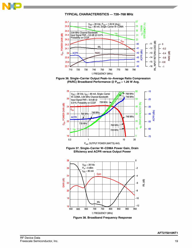
TYPICAL CHARACTERISTICS — 728--768 MHz
16
Pout, OUTPUT POWER (WATTS) AVG.
--10
--20
D,DRAINEFFICIENCY(%)
Gps,POWER
GAIN(dB)
--60
ACPR
(dBc)
--30
--40
--50
28
f, FREQUENCY (MHz)
24
22
20
GAIN(dB)
26
18
550 600 650 750 800 950--12
0
--2
--4
--6
--8
IRL(dB)
--10
IRL,INPUTRETURNLOSS
(dB)
710
f, FREQUENCY (MHz)
Figure 36. Single--Carrier Output Peak--to--Average Ratio Compression(PARC) Broadband Performance @ Pout = 1.26 W Avg.
--15
--11
--12
--13
--14
23.7
24.7
24.6
--45
26
25
24
--40
--41
--42
--43
D,DRAIN
EFFICIENCY(%)
Gps,POWER
GAIN(dB) 24.4
24.2
24.1
24
23.9
720 730 740 750 760 770 780 790
23
--44
--16
ACPR
(dBc)
PARC(dB)
--0.8
0
--0.2
--0.4
--0.6
--1
Figure 37. Single--Carrier W--CDMA Power Gain, DrainEfficiency and ACPR versus Output Power
Figure 38. Broadband Frequency Response
0.3
ACPR
16
28
0
60
50
40
30
20
D
24
10
10
22
20
768 MHz
700 850 900
ACPR
D
PARC
VDD = 28 Vdc, Pout = 1.26 W (Avg.)IDQ = 80 mA, Single--Carrier W--CDMA
IRL
Gps
3.84 MHz Channel BandwidthInput Signal PAR = 9.9 dB @ 0.01%Probability on CCDF
728 MHz
748 MHz
748 MHz
1
VDD = 28 VdcPin = 0 dBmIDQ = 80 mA
Gain
IRL
Gps
VDD = 28 Vdc, IDQ = 80 mA, Single--CarrierW--CDMA, 3.84 MHz Channel BandwidthInput Signal PAR = 9.9 dB @0.01% Probability on CCDF
24.5
24.3
23.8
27
20--70
728 MHz26
18
768 MHz728 MHz
748 MHz768 MHz
20RF Device Data
Freescale Semiconductor, Inc.
AFT27S010NT1
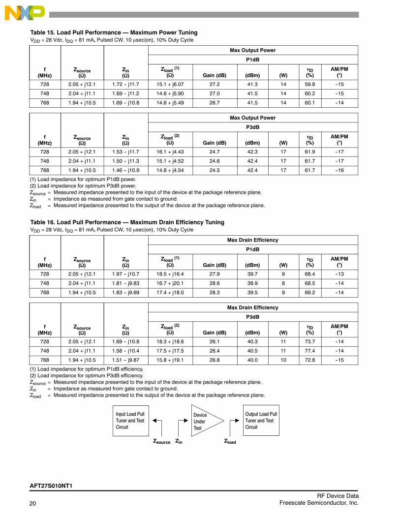
Table 15. Load Pull Performance — Maximum Power TuningVDD = 28 Vdc, IDQ = 81 mA, Pulsed CW, 10 sec(on), 10% Duty Cycle
f(MHz)
Zsource()
Zin()
Max Output Power
P1dB
Zload (1)
() Gain (dB) (dBm) (W)D(%)
AM/PM()
728 2.05 + j12.1 1.72 -- j11.7 15.1 + j6.07 27.2 41.3 14 59.8 --15
748 2.04 + j11.1 1.69 -- j11.2 14.6 + j5.90 27.0 41.5 14 60.2 --15
768 1.94 + j10.5 1.69 -- j10.8 14.6 + j5.49 26.7 41.5 14 60.1 --14
f(MHz)
Zsource()
Zin()
Max Output Power
P3dB
Zload (2)
() Gain (dB) (dBm) (W)D(%)
AM/PM()
728 2.05 + j12.1 1.53 -- j11.7 16.1 + j4.43 24.7 42.3 17 61.9 --17
748 2.04 + j11.1 1.50 -- j11.3 15.1 + j4.52 24.6 42.4 17 61.7 --17
768 1.94 + j10.5 1.46 -- j10.9 14.8 + j4.54 24.5 42.4 17 61.7 --16
(1) Load impedance for optimum P1dB power.(2) Load impedance for optimum P3dB power.Zsource = Measured impedance presented to the input of the device at the package reference plane.Zin = Impedance as measured from gate contact to ground.Zload = Measured impedance presented to the output of the device at the package reference plane.
Table 16. Load Pull Performance — Maximum Drain Efficiency TuningVDD = 28 Vdc, IDQ = 81 mA, Pulsed CW, 10 sec(on), 10% Duty Cycle
f(MHz)
Zsource()
Zin()
Max Drain Efficiency
P1dB
Zload (1)
() Gain (dB) (dBm) (W)D(%)
AM/PM()
728 2.05 + j12.1 1.97 -- j10.7 18.5 + j16.4 27.9 39.7 9 68.4 --13
748 2.04 + j11.1 1.81 -- j9.83 16.7 + j20.1 28.6 38.9 8 68.5 --14
768 1.94 + j10.5 1.83 -- j9.69 17.4 + j18.0 28.3 39.5 9 69.2 --14
f(MHz)
Zsource()
Zin()
Max Drain Efficiency
P3dB
Zload (2)
() Gain (dB) (dBm) (W)D(%)
AM/PM()
728 2.05 + j12.1 1.69 -- j10.8 18.3 + j18.6 26.1 40.3 11 73.7 --14
748 2.04 + j11.1 1.58 -- j10.4 17.5 + j17.5 26.4 40.5 11 77.4 --14
768 1.94 + j10.5 1.51 -- j9.87 15.8 + j19.1 26.8 40.0 10 72.8 --15
(1) Load impedance for optimum P1dB efficiency.(2) Load impedance for optimum P3dB efficiency.Zsource = Measured impedance presented to the input of the device at the package reference plane.Zin = Impedance as measured from gate contact to ground.Zload = Measured impedance presented to the output of the device at the package reference plane.
Input Load PullTuner and TestCircuit
DeviceUnderTest
Zsource Zin Zload
Output Load PullTuner and TestCircuit
AFT27S010NT1
21RF Device DataFreescale Semiconductor, Inc.
P1dB -- TYPICAL LOAD PULL CONTOURS — 748 MHz
--5
25
15
14 16 1810 24
20
10
5
20
0
12 22
IMAGINARY()
--5
25
15
14 16 1810 24
20
10
5
20
0
12 22
--5
25
15
14 16 1810 24
20
10
5
20
0
12 22
NOTE: = Maximum Output Power
= Maximum Drain Efficiency
P
E
Gain
Drain Efficiency
Linearity
Output Power
Figure 39. P1dB Load Pull Output Power Contours (dBm)
REAL ()
--5
25
15
IMAGINARY()
14 16 1810 24
20
10
5
20
0
12
Figure 40. P1dB Load Pull Efficiency Contours (%)
REAL ()
Figure 41. P1dB Load Pull Gain Contours (dB)
REAL ()
Figure 42. P1dB Load Pull AM/PM Contours ()
REAL ()
22
IMAGINARY()
IMAGINARY()
39
P
E38.5
41
40.540
37.5 38
39.5
40
40.5
P
E
5856
5452
6062
64
66
68
66
P
E
2726.5
27.52828.5
2929.530
30.5
P
E
--22
--20 --18
--16
--14
--12--10
22RF Device Data
Freescale Semiconductor, Inc.
AFT27S010NT1
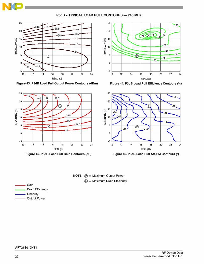
P3dB -- TYPICAL LOAD PULL CONTOURS — 748 MHz
--5
25
15
14 16 1810 24
20
10
5
20
0
12 22
IMAGINARY()
--5
25
15
14 16 1810 24
20
10
5
20
0
12 22
--5
25
15
14 16 1810 24
20
10
5
20
0
12 22
NOTE: = Maximum Output Power
= Maximum Drain Efficiency
P
E
Gain
Drain Efficiency
Linearity
Output Power
Figure 43. P3dB Load Pull Output Power Contours (dBm)
REAL ()
--5
25
15
IMAGINARY()
14 16 1810 24
20
10
5
20
0
12
Figure 44. P3dB Load Pull Efficiency Contours (%)
REAL ()
Figure 45. P3dB Load Pull Gain Contours (dB)
REAL ()
Figure 46. P3dB Load Pull AM/PM Contours ()
REAL ()
22
IMAGINARY()
IMAGINARY()
P
E
41.541
42
38.5 39 39.5 40
40.5
41
41.5
P
E
6062
6466
68
707274
76
68
P
E
24.5
24
25
25.5
26
26.52727.528
P
E
--8
--10
--12
--14
--16--18
--20--22
--24
AFT27S010NT1
23RF Device DataFreescale Semiconductor, Inc.
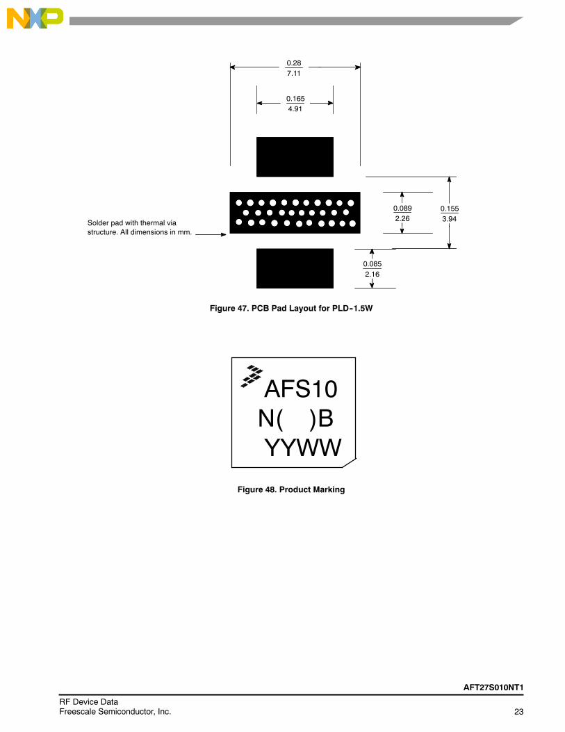
Figure 47. PCB Pad Layout for PLD--1.5W
7.110.28
4.910.165
3.940.155
2.260.089
2.160.085
Solder pad with thermal viastructure. All dimensions in mm.
Figure 48. Product Marking
AFS10N( )BYYWW
24RF Device Data
Freescale Semiconductor, Inc.
AFT27S010NT1
PACKAGE DIMENSIONS
AFT27S010NT1
25RF Device DataFreescale Semiconductor, Inc.
26RF Device Data
Freescale Semiconductor, Inc.
AFT27S010NT1
AFT27S010NT1
27RF Device DataFreescale Semiconductor, Inc.
PRODUCT DOCUMENTATION, SOFTWARE AND TOOLS
Refer to the following resources to aid your design process.
Application Notes AN1955: Thermal Measurement Methodology of RF Power Amplifiers
Software Electromigration MTTF Calculator
RF High Power Model
.s2p File
Development Tools Printed Circuit Boards
For Software and Tools, do a Part Number search at http://www.freescale.com, and select the “Part Number” link. Go toSoftware & Tools on the part’s Product Summary page to download the respective tool.
REVISION HISTORY
The following table summarizes revisions to this document.
Revision Date Description
0 Nov. 2013 Initial Release of Data Sheet
1 Sept. 2014 Tape and Reel information: corrected tape width information from 13--inch reel to 7--inch reel to reflectactual reel size, p. 1
Changed operating frequency from 728–2700 MHz to 728–3600 MHz due to expanded device frequencycapability resulting from additional test data, p. 1
2 Nov. 2014 Added 3400--3600 MHz performance information as follows:-- Typical Frequency Band table, p. 1-- Fig. 32, Single--Carrier Output Peak--to--Average Ratio Compression (PARC) Broadband Performance@ Pout = 1.26 W Avg., p. 17
-- Fig. 33, Single--Carrier W--CDMA Power Gain, Drain Efficiency and ACPR versus Output Power, p. 17-- Fig. 34, Broadband Frequency Response, p. 17
3 Dec. 2015 Table 1, Maximum Ratings: corrected operating junction temperature range upper limit, p. 2
Table 5, Electrical Characteristics, On Characteristics VDS(on): updated ID unit of measure to mAdc toreflect actual unit of measure, p. 2
Added Ordering Information Table 6, p. 3
28RF Device Data
Freescale Semiconductor, Inc.
AFT27S010NT1
Information in this document is provided solely to enable system and softwareimplementers to use Freescale products. There are no express or implied copyrightlicenses granted hereunder to design or fabricate any integrated circuits based on theinformation in this document.
Freescale reserves the right to make changes without further notice to any productsherein. Freescale makes no warranty, representation, or guarantee regarding thesuitability of its products for any particular purpose, nor does Freescale assume anyliability arising out of the application or use of any product or circuit, and specificallydisclaims any and all liability, including without limitation consequential or incidentaldamages. “Typical” parameters that may be provided in Freescale data sheets and/orspecifications can and do vary in different applications, and actual performance mayvary over time. All operating parameters, including “typicals,” must be validated foreach customer application by customer’s technical experts. Freescale does not conveyany license under its patent rights nor the rights of others. Freescale sells productspursuant to standard terms and conditions of sale, which can be found at the followingaddress: freescale.com/SalesTermsandConditions.
Freescale and the Freescale logo are trademarks of Freescale Semiconductor, Inc.,Reg. U.S. Pat. & Tm. Off. Airfast is a trademark of Freescale Semiconductor, Inc. Allother product or service names are the property of their respective owners.E 2013–2015 Freescale Semiconductor, Inc.
How to Reach Us:
Home Page:freescale.com
Web Support:freescale.com/support
Document Number: AFT27S010NRev. 3, 12/2015