N RCHIVE INFORMATION - NXP...
12
ARCHIVE INFORMATION ARCHIVE INFORMATION Indium Gallium Phosphorus HBT WLAN Power Amplifier Designed for 802.11g and dual mode applications with frequencies from 2400 to 2500 MHz. • 26.5 dBm P1dB @ 2450 MHz • Power Gain: 27.5 dB Typ (@ f = 2450 MHz, Class AB) • High Gain, High Efficiency and High Linearity • EVM = 3% Typ @ P out = +19 dBM, 14% PAE • RoHS Compliant • In Tape and Reel. R2 Suffix = 1,500 Units per 12 mm, 7 inch Reel. Table 1. Maximum Ratings Rating Symbol Value Unit Collector Supply V CC 5 V Base Supply First Stage V B1 5 V Base Supply Second Stage V B2 5 V Detector Bias Supply V BIAS 5 V DC Current I DC 171 mA Table 2. Thermal Characteristics Characteristic Symbol Value Unit Thermal Resistance, Junction to Case R θJC 185 (1) °C/W Case Operating Temperature Range T C --40 to +85 °C Storage Temperature Range T stg --55 to +150 °C Table 3. ESD Protection Characteristics Test Methodology Class Human Body Model (per JESD22--A114) 2 (Minimum) Machine Model (per EIA/JESD22--A115) A (Minimum) Charge Device Model (per JESD22--C101) II (Minimum) Table 4. Moisture Sensitivity Level Test Methodology Rating Package Peak Temperature Unit Per JESD 22--A113, IPC/JEDEC J--STD--020 1 260 °C 1. Simulated. Document Number: MMG2401 Rev. 3, 5/2006 Freescale Semiconductor Technical Data 2400--2500 MHz, 27.5 dB, 26.5 dBm 802.11g WLAN POWER AMPLIFIER InGaP HBT MMG2401NR2 CASE 1483--01 QFN 3x3 © Freescale Semiconductor, Inc., 2006, 2008. All rights reserved.
Transcript of N RCHIVE INFORMATION - NXP...

ARCHIVEINFORMATION
ARCHIVEINFORMATION
MMG2401NR2
1RF Device DataFreescale Semiconductor
Indium Gallium Phosphorus HBTWLAN Power AmplifierDesigned for 802.11g and dual mode applications with frequencies from
2400 to 2500 MHz.
• 26.5 dBm P1dB @ 2450 MHz
• Power Gain: 27.5 dB Typ (@ f = 2450 MHz, Class AB)
• High Gain, High Efficiency and High Linearity• EVM = 3% Typ @ Pout = +19 dBM, 14% PAE• RoHS Compliant• In Tape and Reel. R2 Suffix = 1,500 Units per 12 mm, 7 inch Reel.
Table 1. Maximum Ratings
Rating Symbol Value Unit
Collector Supply VCC 5 V
Base Supply First Stage VB1 5 V
Base Supply Second Stage VB2 5 V
Detector Bias Supply VBIAS 5 V
DC Current IDC 171 mA
Table 2. Thermal Characteristics
Characteristic Symbol Value Unit
Thermal Resistance, Junction to Case RθJC 185 (1) °C/W
Case Operating Temperature Range TC -- 40 to +85 °C
Storage Temperature Range Tstg -- 55 to +150 °C
Table 3. ESD Protection Characteristics
Test Methodology Class
Human Body Model (per JESD22--A114) 2 (Minimum)
Machine Model (per EIA/JESD22--A115) A (Minimum)
Charge Device Model (per JESD22--C101) II (Minimum)
Table 4. Moisture Sensitivity Level
Test Methodology Rating Package Peak Temperature Unit
Per JESD 22--A113, IPC/JEDEC J--STD--020 1 260 °C
1. Simulated.
Document Number: MMG2401Rev. 3, 5/2006
Freescale SemiconductorTechnical Data
2400--2500 MHz, 27.5 dB, 26.5 dBm802.11g WLAN POWER AMPLIFIER
InGaP HBT
MMG2401NR2
CASE 1483--01QFN 3x3
© Freescale Semiconductor, Inc., 2006, 2008. All rights reserved.
ARCHIVEINFORMATION
ARCHIVEINFORMATION
2RF Device Data
Freescale Semiconductor
MMG2401NR2
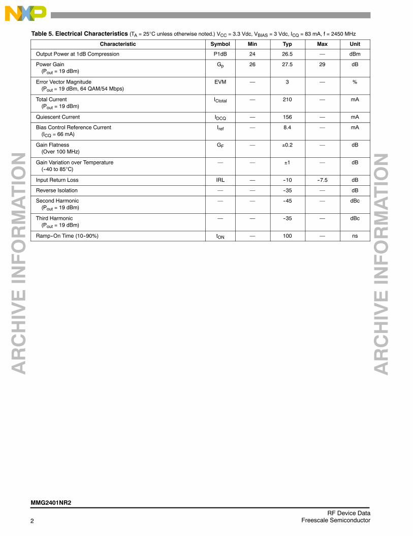
Table 5. Electrical Characteristics (TA = 25°C unless otherwise noted.) VCC = 3.3 Vdc, VBIAS = 3 Vdc, ICQ = 83 mA, f = 2450 MHz
Characteristic Symbol Min Typ Max Unit
Output Power at 1dB Compression P1dB 24 26.5 � dBm
Power Gain(Pout = 19 dBm)
Gp 26 27.5 29 dB
Error Vector Magnitude(Pout = 19 dBm, 64 QAM/54 Mbps)
EVM � 3 � %
Total Current(Pout = 19 dBm)
ICtotal � 210 � mA
Quiescent Current IDCQ � 156 � mA
Bias Control Reference Current(ICQ = 66 mA)
Iref � 8.4 � mA
Gain Flatness(Over 100 MHz)
GF � ±0.2 � dB
Gain Variation over Temperature(--40 to 85°C)
� � ±1 � dB
Input Return Loss IRL � --10 --7.5 dB
Reverse Isolation � � --35 � dB
Second Harmonic(Pout = 19 dBm)
� � --45 � dBc
Third Harmonic(Pout = 19 dBm)
� � --35 � dBc
Ramp--On Time (10--90%) tON � 100 � ns

ARCHIVEINFORMATION
ARCHIVEINFORMATION
MMG2401NR2
3RF Device DataFreescale Semiconductor
Table 6. Functional Pin Description
Name PinNumber
Description
VB1 1 Base power supply for first stage amplifier.
RFIN 2, 3 RF input for the power amplifier. This pin is DC--shorted toGND and AC--coupled to the transistor base of the firststage.
VBIAS 4 Detector bias voltage supply.
VREF 5 Detector output voltage reference. Vout -- VREF is useful fortracking detector performance over temperature.
VOUT 6 Detector output voltage.
VCC2 7 Collector power supply for second stage amplifier.
RFOUT 8, 9 RF output for the power amplifier. This pin is DC--coupledand requires a DC--blocking series capacitor.
VB2 10 Base power supply for second stage amplifier.
NC 11 Not connected.
VCC1 12 Collector power supply for first stage amplifier.
GND BacksideCenterMetal
The center metal base of the QFN 3x3 package providesboth DC and RF ground as well as heat sink contact for thepower amplifier.
Figure 1. Pin Connections
9
8
7
6
(Top View)
VOUT
RFIN
RFIN
1
2
3
54
101112VB2
VREF
VB1
NCVCC1
RFOUTRFOUTVCC2
VBIAS
ARCHIVEINFORMATION
ARCHIVEINFORMATION
4RF Device Data
Freescale Semiconductor
MMG2401NR2
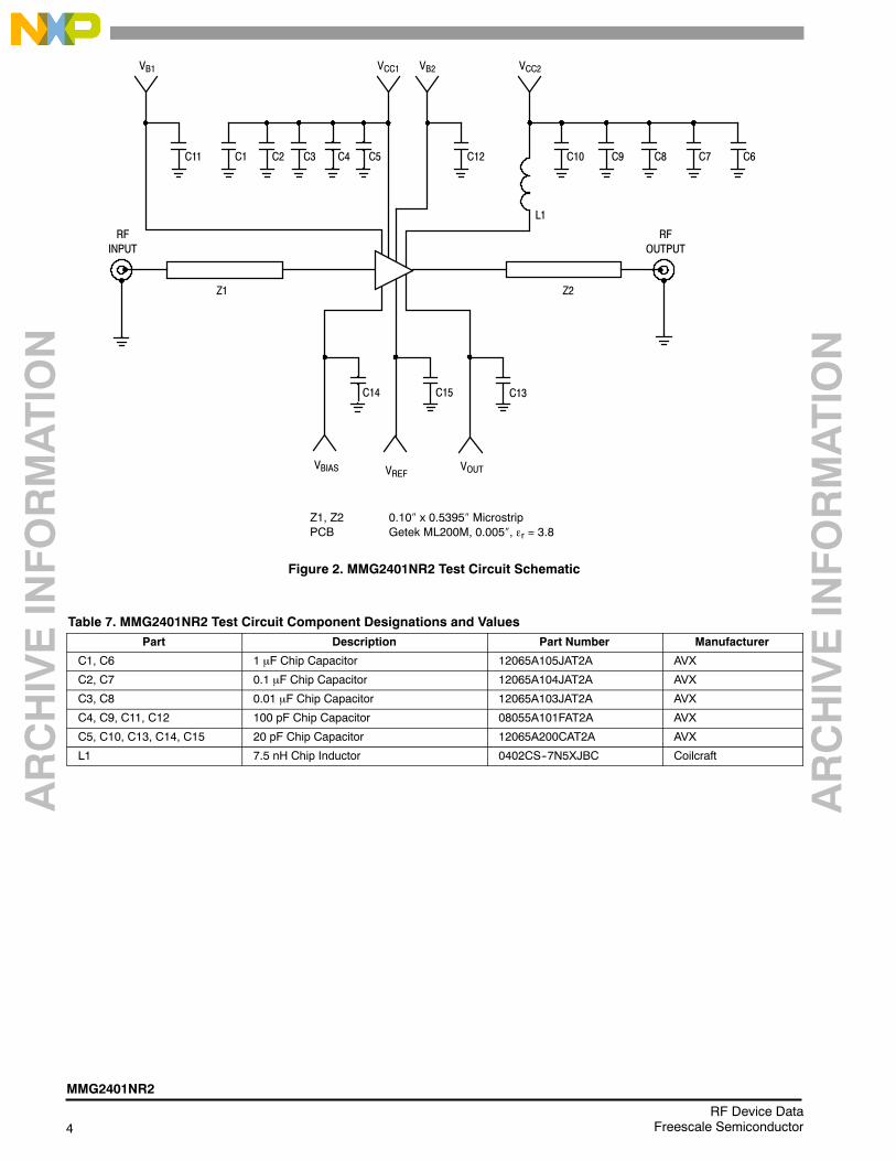
Figure 2. MMG2401NR2 Test Circuit Schematic
Z1, Z2 0.10″ x 0.5395″ MicrostripPCB Getek ML200M, 0.005″, εr = 3.8
C11 C1 C2 C3 C4 C5 C12 C10 C9 C8 C7 C6
L1
VCC2VCC1VB1
Z1
RFINPUT
RFOUTPUT
C14 C15 C13
VBIAS VREFVOUT
Z2
VB2
Table 7. MMG2401NR2 Test Circuit Component Designations and ValuesPart Description Part Number Manufacturer
C1, C6 1 μF Chip Capacitor 12065A105JAT2A AVX
C2, C7 0.1 μF Chip Capacitor 12065A104JAT2A AVX
C3, C8 0.01 μF Chip Capacitor 12065A103JAT2A AVX
C4, C9, C11, C12 100 pF Chip Capacitor 08055A101FAT2A AVX
C5, C10, C13, C14, C15 20 pF Chip Capacitor 12065A200CAT2A AVX
L1 7.5 nH Chip Inductor 0402CS--7N5XJBC Coilcraft

ARCHIVEINFORMATION
ARCHIVEINFORMATION
MMG2401NR2
5RF Device DataFreescale Semiconductor
Figure 3. MMG2401NR2 Test Circuit Component Layout
Freescale has begun the transition of marking Printed Circuit Boards (PCBs) with the Freescale Semiconductorsignature/logo. PCBs may have either Motorola or Freescale markings during the transition period. These changes will haveno impact on form, fit or function of the current product.
VB1
C1
C12
C2
C3
C4
C5
C11
VB2
VCC1
C14C15 C13
C10
C9
C8
C7
C6
VBIAS VREF VOUT
VCC2
L1

ARCHIVEINFORMATION
ARCHIVEINFORMATION
6RF Device Data
Freescale Semiconductor
MMG2401NR2
TYPICAL CHARACTERISTICS
2524
29
0
TC = 25_C
Pout, OUTPUT POWER (dBm)
Figure 4. Power Gain versus Output Power
VCC = 3.3 VdcVB1 = 2.9 Vdcf = 2450 MHz
--40_C
85_C
28
27
26
25
5 10 15 20 250
7
0
Pout, OUTPUT POWER (dBm)
Figure 5. Error Vector Magnitude versusOutput Power
TC = 25_C
VCC = 3.3 VdcVB1 = 2.9 Vdcf = 2450 MHz
--40_C
85_C
EVM,ERRORVECTORMAGNITUDE(%)
6
5
4
3
2
1
5 10 15 20
TC = --40_C
250
25
0
Pout, OUTPUT POWER (dBm)
Figure 6. Efficiency versus Output Power
VCC = 3.3 VdcVB1 = 2.9 Vdcf = 2450 MHz
25_C
85_C
20
15
10
5
5 10 15 20 250.01
10
0
Pout, OUTPUT POWER (dBm)
Figure 7. Detector Output Voltage versusOutput Power
V out,DETECTOROUTPUTVOLTAGE(V)
TC = 85_C
VCC = 3.3 VdcVB1 = 2.9 Vdcf = 2450 MHz
25_C--40_C
1
0.1
5 10 15 20
30--4
4
0
Pout, OUTPUT POWER (dBm)
Figure 8. AM to PM versus Output Power
AMtoPM
(_)
3
2
1
0
--1
--2
--3
5 10 15 20
VCC = 3.3 VdcVB1 = 2.9 Vdcf = 2450 MHz
25 250
250
0
Pout, OUTPUT POWER (dBm)
Figure 9. Total Current versus Output Power
I CC,TOTALCURRENT(mA)
TC = 85_C
VCC = 3.3 VdcVB1 = 2.9 Vdcf = 2450 MHz
25_C
--40_C
200
150
100
50
5 10 15 20
Gp,POWER
GAIN(dB)
η,EFFICIENCY(%)

ARCHIVEINFORMATION
ARCHIVEINFORMATION
MMG2401NR2
7RF Device DataFreescale Semiconductor
TYPICAL CHARACTERISTICS
2.810
35
2
f, FREQUENCY (GHz)
Figure 10. Power Gain (S21) versusFrequency
Gp,
POWER
GAIN(dB)
VCC = 3.3 VdcVB1 = 2.9 Vdc
30
25
20
15
2.1 2.2 2.3 2.4 2.5 2.6 2.7 2.8--25
0
2
--5
--10
--15
--20
2.1 2.2 2.3 2.4 2.5 2.6 2.7
f, FREQUENCY (GHz)
Figure 11. Input Return Loss (S11) versusFrequency
INPUTRETURNLOSS
(dB)
IRL,
VCC = 3.3 VdcVB1 = 2.9 Vdc
2.8--70
--20
2
--30
--40
--50
--60
2.1 2.2 2.3 2.4 2.5 2.6 2.7
VCC = 3.3 VdcVB1 = 2.9 Vdc
f, FREQUENCY (GHz)
Figure 12. Reverse TransconductanceIsolation (S12) versus Frequency
REVERSE
TRANSCONDUCTANCEISOLATION(dB)
2.8--25
0
2
--5
--10
--15
--20
2.1 2.2 2.3 2.4 2.5 2.6 2.7
f, FREQUENCY (GHz)
Figure 13. Output Return Loss (S22) versusFrequency
ORL,OUTPUTRETURNLOSS
(dB)
VCC = 3.3 VdcVB1 = 2.9 Vdc
ARCHIVEINFORMATION
ARCHIVEINFORMATION
8RF Device Data
Freescale Semiconductor
MMG2401NR2
EXPOSED PAD
SYMBOLSMIN MAX
1
Figure 14. MMG2401NR2 Specific Mechanical Outline Information
TOP VIEW BOTTOM VIEWSIDE VIEW
0.25 MIN.
0.45
0.25 MIN.
23
1B
A
C
L
4X D
4X D
(Ny--1)eF2F/23
e
(Nx--1)e
PIN1 ID
E/2E
1
N=12
b
SEATINGPLANE
STANDARD
DETAIL �A� -- PIN #1 ID AND TIE BAR MARK OPTION
NOTES:
1. DIMENSION b APPLIES TO PLATED TERMINAL AND ISMEASURED BETWEEN 0.20 AND 0.25 MM FROMTERMINAL TIP.
2. N IS THE NUMBER OF TERMINALS (12).Nx IS THE NUMBER OF TERMINALS IN X--DIRECTIONANDNy IS THE NUMBER OF TERMINALS IN Y--DIRECTION.
3. ALL DIMENSIONS ARE IN MILLIMETERS.
2
2
DIMA
MIN NOM MAX3.00 BSC
B 3.00 BSCC -- 0.85 1.00D 0.24 0.42 0.60EF
0.18 0.23be 0.50 BSC
Ny 3
SEE EXPOSED PAD
Nx
SEE EXPOSED PAD
3
0.30
NOME
1.30MIN NOM MAX
F
1.301.15 1.45 1.15 1.45

ARCHIVEINFORMATION
ARCHIVEINFORMATION
MMG2401NR2
9RF Device DataFreescale Semiconductor
PACKAGE DIMENSIONS
B
3
3
A
2X
0.1 C
C0.1
2X
PIN 1 INDEXAREA
EXPOSED DIEATTACH PAD
10 12
6 4
9
7
1
3
0.10
8X 0.512X
9
DETAIL G
M
M
1.551.25
1.551.25
0.300.18
12X
DETAIL M
DETAIL N
PIN 1 INDEX
0.750.50
C A B
VIEW M -- M
M
NOTES:1. ALL DIMENSIONS ARE IN MILLIMETERS.2. INTERPRET DIMENSIONS AND
TOLERANCES PER ASME Y14.5M, 1994.3. THE COMPLETE JEDEC DESIGNATOR FOR
THIS PACKAGE IS: HF--PQFP--N.4. FOR ANVIL SINGULATED QFN PACKAGES,
MAXIMUM DRAFT ANGLED IS 12 .5. PACKAGE WARPAGE MAX 0.05 MM.6. CORNER CHAMFER MAY NOT BE PRESENT.
DIMENSIONS OF OPTIONAL FEATURES AREFOR REFERENCE ONLY.
7. CORNER LEADS CAN BE USED FORTHERMAL OR GROUND AND ARE TIED TOTHE DIE ATTACH PAD. THESE LEADS ARENOT INCLUDED IN THE LEAD COUNT.
8. COPLANARITY APPLIES TO LEAD, CORNERLEADS, AND DIE ATTACH PAD.
9. THIS DIMENSION APPLIES TO PLATEDTERMINAL AND IS MEASURED BETWEEN0.20 MM AND 0.25 MM FROM TERMINAL TIP.
_
CASE 1483--01ISSUE AQFN 3x3 Page 1 of 3

ARCHIVEINFORMATION
ARCHIVEINFORMATION
10RF Device Data
Freescale Semiconductor
MMG2401NR2
6
DETAIL NPREFERRED CORNER CONFIGURATION
6
DETAIL NCORNER CONFIGURATION
_(45 )
(0.25) (0.25)
0.600.24
0.600.24
CASE 1483--01ISSUE AQFN 3x3
8
DETAIL GVIEW ROTATED 90 CW
1.00.8
_
1.000.75
0.050.00 SEATING
PLANEC
0.1
0.05
C
C
Page 2 of 3
ARCHIVEINFORMATION
ARCHIVEINFORMATION
MMG2401NR2
11RF Device DataFreescale Semiconductor
CASE 1483--01ISSUE AQFN 3x3
_(45 )
DETAIL MPREFERRED BACKSIDE PIN 1 INDEX
0.650.30
TIE BAR MARK OPTION7
PIN 1 ID
4X 0.230.13
4X
(0.35)
DETAIL M
BACKSIDE PIN 1 INDEX OPTION
DETAIL S
DETAIL M
BACKSIDE PIN 1 INDEX OPTION
(0.45)
PIN 1 IDR0.2
DETAIL SBACKSIDE PIN 1 INDEX
0.2170.137
(0.25)
0.2170.137
(0.1)
(0.25)
Page 3 of 3

ARCHIVEINFORMATION
ARCHIVEINFORMATION
12RF Device Data
Freescale Semiconductor
MMG2401NR2
Information in this document is provided solely to enable system and softwareimplementers to use Freescale Semiconductor products. There are no express orimplied copyright licenses granted hereunder to design or fabricate any integratedcircuits or integrated circuits based on the information in this document.
Freescale Semiconductor reserves the right to make changes without further notice toany products herein. Freescale Semiconductor makes no warranty, representation orguarantee regarding the suitability of its products for any particular purpose, nor doesFreescale Semiconductor assume any liability arising out of the application or use ofany product or circuit, and specifically disclaims any and all liability, including withoutlimitation consequential or incidental damages. �Typical� parameters that may beprovided in Freescale Semiconductor data sheets and/or specifications can and dovary in different applications and actual performance may vary over time. All operatingparameters, including �Typicals�, must be validated for each customer application bycustomer�s technical experts. Freescale Semiconductor does not convey any licenseunder its patent rights nor the rights of others. Freescale Semiconductor products arenot designed, intended, or authorized for use as components in systems intended forsurgical implant into the body, or other applications intended to support or sustain life,or for any other application in which the failure of the Freescale Semiconductor productcould create a situation where personal injury or death may occur. Should Buyerpurchase or use Freescale Semiconductor products for any such unintended orunauthorized application, Buyer shall indemnify and hold Freescale Semiconductorand its officers, employees, subsidiaries, affiliates, and distributors harmless against allclaims, costs, damages, and expenses, and reasonable attorney fees arising out of,directly or indirectly, any claim of personal injury or death associated with suchunintended or unauthorized use, even if such claim alleges that FreescaleSemiconductor was negligent regarding the design or manufacture of the part.
Freescalet and the Freescale logo are trademarks of Freescale Semiconductor, Inc.All other product or service names are the property of their respective owners.© Freescale Semiconductor, Inc. 2006, 2008. All rights reserved.
How to Reach Us:
Home Page:www.freescale.com
E--mail:[email protected]
USA/Europe or Locations Not Listed:Freescale SemiconductorTechnical Information Center, CH3701300 N. Alma School RoadChandler, Arizona 85224+1--800--521--6274 or [email protected]
Europe, Middle East, and Africa:Freescale Halbleiter Deutschland GmbHTechnical Information CenterSchatzbogen 781829 Muenchen, Germany+44 1296 380 456 (English)+46 8 52200080 (English)+49 89 92103 559 (German)+33 1 69 35 48 48 (French)[email protected]
Japan:Freescale Semiconductor Japan Ltd.HeadquartersARCO Tower 15F1--8--1, Shimo--Meguro, Meguro--ku,Tokyo 153--0064Japan0120 191014 or +81 3 5437 [email protected]
Asia/Pacific:Freescale Semiconductor Hong Kong Ltd.Technical Information Center2 Dai King StreetTai Po Industrial EstateTai Po, N.T., Hong Kong+800 2666 [email protected]
For Literature Requests Only:Freescale Semiconductor Literature Distribution CenterP.O. Box 5405Denver, Colorado 802171--800--441--2447 or 303--675--2140Fax: [email protected]
Document Number: MMG2401Rev. 3, 5/2006