
RF Power LDMOS Transistor - NXP...
24
RF Power LDMOS Transistor N--Channel Enhancement--Mode Lateral MOSFET This 63 W asymmetrical Doherty RF power LDMOS transistor is designed for cellular base station applications covering the frequency range of 1805 to 1995 MHz. 1800 MHz Typical Doherty Single--Carrier W--CDMA Performance: V DD = 28 Vdc, I DQA = 800 mA, V GSB = 0.7 Vdc, P out = 63 W Avg., Input Signal PAR = 9.9 dB @ 0.01% Probability on CCDF. G ps (dB) D (%) Output PAR (dB) ACPR (dBc) 1805 MHz 17.3 50.3 7.8 --34.6 1840 MHz 17.5 49.7 7.9 --37.4 1880 MHz 17.4 50.3 7.8 --37.6 1900 MHz Typical Doherty Single--Carrier W--CDMA Performance: V DD = 28 Vdc, I DQA = 800 mA, V GSB = 0.4 Vdc, P out = 63 W Avg., Input Signal PAR = 9.9 dB @ 0.01% Probability on CCDF. Frequency G ps (dB) D (%) Output PAR (dB) ACPR (dBc) 1930 MHz 17.0 49.1 7.7 --34.6 1960 MHz 17.1 48.9 7.6 --37.4 1995 MHz 17.0 49.1 7.4 --37.6 Features Advanced High Performance In--Package Doherty Greater Negative Gate--Source Voltage Range for Improved Class C Operation Designed for Digital Predistortion Error Correction Systems In Tape and Reel. R6 Suffix = 150 Units, 56 mm Tape Width, 13--inch Reel. Document Number: AFT18H357--24S Rev. 0, 3/2014 Freescale Semiconductor Technical Data 1805–1995 MHz, 63 W AVG., 28 V AIRFAST RF POWER LDMOS TRANSISTOR AFT18H357--24SR6 NI--1230S--4L2L (Top View) RF outA /V DSA RF outB /V DSB RF inA /V GSA RF inB /V GSB VBW A (1) 6 3 1 5 2 4 Carrier Peaking Figure 1. Pin Connections VBW B (1) 1. Device cannot operate with the V DD current supplied through pin 3 and pin 6. Freescale Semiconductor, Inc., 2014. All rights reserved.
Transcript of RF Power LDMOS Transistor - NXP...

AFT18H357--24SR6
1RF Device DataFreescale Semiconductor, Inc.
RF Power LDMOS TransistorN--Channel Enhancement--Mode Lateral MOSFETThis 63 W asymmetrical Doherty RF power LDMOS transistor is designed
for cellular base station applications covering the frequency range of 1805 to1995 MHz.
1800 MHz
Typical Doherty Single--Carrier W--CDMA Performance: VDD = 28 Vdc,IDQA = 800 mA, VGSB = 0.7 Vdc, Pout = 63 W Avg., Input SignalPAR = 9.9 dB @ 0.01% Probability on CCDF.
Gps(dB)
D(%)
Output PAR(dB)
ACPR(dBc)
1805 MHz 17.3 50.3 7.8 --34.6
1840 MHz 17.5 49.7 7.9 --37.4
1880 MHz 17.4 50.3 7.8 --37.6
1900 MHz
Typical Doherty Single--Carrier W--CDMA Performance: VDD = 28 Vdc,IDQA = 800 mA, VGSB = 0.4 Vdc, Pout = 63 W Avg., Input SignalPAR = 9.9 dB @ 0.01% Probability on CCDF.
FrequencyGps(dB)
D(%)
Output PAR(dB)
ACPR(dBc)
1930 MHz 17.0 49.1 7.7 --34.6
1960 MHz 17.1 48.9 7.6 --37.4
1995 MHz 17.0 49.1 7.4 --37.6
Features Advanced High Performance In--Package Doherty Greater Negative Gate--Source Voltage Range for Improved Class C
Operation Designed for Digital Predistortion Error Correction Systems In Tape and Reel. R6 Suffix = 150 Units, 56 mm Tape Width, 13--inch Reel.
Document Number: AFT18H357--24SRev. 0, 3/2014
Freescale SemiconductorTechnical Data
1805–1995 MHz, 63 W AVG., 28 VAIRFAST RF POWER LDMOS
TRANSISTOR
AFT18H357--24SR6
NI--1230S--4L2L
(Top View)
RFoutA/VDSA
RFoutB/VDSB
RFinA/VGSA
RFinB/VGSB
VBWA(1)6
3
1 5
2 4
Carrier
Peaking
Figure 1. Pin Connections
VBWB(1)
1. Device cannot operate with the VDDcurrent supplied through pin 3 and pin 6.
Freescale Semiconductor, Inc., 2014. All rights reserved.

2RF Device Data
Freescale Semiconductor, Inc.
AFT18H357--24SR6
Table 1. Maximum Ratings
Rating Symbol Value Unit
Drain--Source Voltage VDSS --0.5, +65 Vdc
Gate--Source Voltage VGS --6.0, +10 Vdc
Operating Voltage VDD 32, +0 Vdc
Storage Temperature Range Tstg --65 to +150 C
Case Operating Temperature Range TC --40 to +150 C
Operating Junction Temperature Range (1,2) TJ --40 to +225 C
CW Operation @ TC = 25CDerate above 25C
CW 3783.24
WW/C
Table 2. Thermal Characteristics
Characteristic Symbol Value (2,3) Unit
Thermal Resistance, Junction to CaseCase Temperature 79C, 63 W W--CDMA, 28 Vdc, IDQA = 800 mA, VGSB = 0.7 Vdc, 1840 MHz
RJC 0.43 C/W
Table 3. ESD Protection Characteristics
Test Methodology Class
Human Body Model (per JESD22--A114) 2
Machine Model (per EIA/JESD22--A115) IV
Charge Device Model (per JESD22--C101) B
Table 4. Electrical Characteristics (TA = 25C unless otherwise noted)
Characteristic Symbol Min Typ Max Unit
Off Characteristics (4)
Zero Gate Voltage Drain Leakage Current(VDS = 65 Vdc, VGS = 0 Vdc)
IDSS — — 10 Adc
Zero Gate Voltage Drain Leakage Current(VDS = 28 Vdc, VGS = 0 Vdc)
IDSS — — 1 Adc
Gate--Source Leakage Current(VGS = 5 Vdc, VDS = 0 Vdc)
IGSS — — 1 Adc
On Characteristics -- Side A (4)
Gate Threshold Voltage(VDS = 10 Vdc, ID = 140 Adc)
VGS(th) 0.8 1.2 1.6 Vdc
Gate Quiescent Voltage(VDD = 28 Vdc, IDA = 800 mAdc, Measured in Functional Test)
VGSA(Q) 1.4 1.8 2.2 Vdc
Drain--Source On--Voltage(VGS = 10 Vdc, ID = 1.4 Adc)
VDS(on) 0.1 0.15 0.3 Vdc
On Characteristics -- Side B (4)
Gate Threshold Voltage(VDS = 10 Vdc, ID = 240 Adc)
VGS(th) 0.8 1.2 1.6 Vdc
Drain--Source On--Voltage(VGS = 10 Vdc, ID = 2.4 Adc)
VDS(on) 0.1 0.15 0.3 Vdc
1. Continuous use at maximum temperature will affect MTTF.2. MTTF calculator available at http://www.freescale.com/rf. Select Software & Tools/Development Tools/Calculators to access MTTF
calculators by product.3. Refer to AN1955, Thermal Measurement Methodology of RF Power Amplifiers. Go to http://www.freescale.com/rf. Select
Documentation/Application Notes -- AN1955.4. Each side of device measured separately.
(continued)

AFT18H357--24SR6
3RF Device DataFreescale Semiconductor, Inc.
Table 4. Electrical Characteristics (TA = 25C unless otherwise noted) (continued)
Characteristic Symbol Min Typ Max Unit
Functional Tests (1,2) (In Freescale Doherty Test Fixture, 50 ohm system) VDD = 28 Vdc, IDQA = 800 mA, VGSB = 0.7 V,Pout = 63 W Avg., f = 1805 MHz, Single--Carrier W--CDMA, IQ Magnitude Clipping, Input Signal PAR = 9.9 dB @ 0.01% Probability on CCDF.ACPR measured in 3.84 MHz Channel Bandwidth @ 5 MHz Offset.
Power Gain Gps 16.6 17.3 19.6 dB
Drain Efficiency D 47.4 50.3 — %
Output Peak--to--Average Ratio @ 0.01% Probability on CCDF PAR 7.4 7.8 — dB
Adjacent Channel Power Ratio ACPR — --34.6 --32.0 dBc
Load Mismatch (In Freescale Test Fixture, 50 ohm system) IDQA = 800 mA, f = 1840 MHz, 10 sec Pulse Width, 10% Duty Cycle
VSWR 10:1 at 32 Vdc, 360 W Pulse Output Power(3 dB Input Overdrive from 210 W Pulse Rated Power)
No Device Degradation
Typical Performance (2) (In Freescale Doherty Test Fixture, 50 ohm system) VDD = 28 Vdc, IDQA = 800 mA, VGSB = 0.7 Vdc,1805–1880 MHz Bandwidth
Pout @ 1 dB Compression Point, CW P1dB — 220 — W
Pout @ 3 dB Compression Point (3) P3dB — 320 — W
AM/PM(Maximum value measured at the P3dB compression point acrossthe 1805--1880 MHz bandwidth)
— --15 —
VBW Resonance Point(IMD Third Order Intermodulation Inflection Point)
VBWres — 110 — MHz
Gain Flatness in 75 MHz Bandwidth @ Pout = 63 W Avg. GF — 0.2 — dB
Gain Variation over Temperature(--30C to +85C)
G — 0.008 — dB/C
Output Power Variation over Temperature(--30C to +85C) (4)
P1dB — 0.009 — dB/C
1. Part internally matched both on input and output.2. Measurements made with device in an asymmetrical Doherty configuration.3. P3dB = Pavg + 7.0 dB where Pavg is the average output power measured using an unclipped W--CDMA single--carrier input signal where
output PAR is compressed to 7.0 dB @ 0.01% probability on CCDF.4. Exceeds recommended operating conditions. See CW operation data in Maximum Ratings table.

4RF Device Data
Freescale Semiconductor, Inc.
AFT18H357--24SR6
Figure 2. AFT18H357--24SR6 Test Circuit Component Layout — 1805–1880 MHz
--
--
AFT18H357--24SRev. 6
C1
D55983
C9
R1
C
PR2
C5
C17C18
C6
Z1
R3
C19
C2C10
C16
C14 C4
C22C12
C8
C20
C7
C21
C3C13
C15
C11
VDDA
VDDB
VGGA
VGGB
CUTOUTAREA
Table 5. AFT18H357--24SR6 Test Circuit Component Designations and Values — 1805–1880 MHzPart Description Part Number Manufacturer
C1, C2, C3, C4 20 pF Chip Capacitors ATC600F200JT250XT ATC
C5, C6 12 pF Chip Capacitors ATC600F120JT250XT ATC
C7, C8 8.2 pF Chip Capacitors ATC600F8R2JT250XT ATC
C9, C10, C11, C12,C13, C14
10 F Chip Capacitors C5750X7S2A106K230KB TDK
C15, C16 220 F, 63 V Electrolytic Capacitors SK063M0220B5S-1015 YAGEO
C17 0.8 pF Chip Capacitor ATC600F0R8BT250XT ATC
C18 0.9 pF Chip Capacitor ATC600F0R9BT250XT ATC
C19 1.2 pF Chip Capacitor ATC600F1R2BT250XT ATC
C20 0.2 pF Chip Capacitor ATC600F0R2BT250XT ATC
C21, C22 2.2 F Chip Capacitors C3225X7R2A225KT TDK
R1, R2 2.2 , 1/4 W Chip Resistors CRCW12062R20JNEA Vishay
R3 50 , 10 W Chip Resistor CW12010T0050GBK ATC
Z1 1700--2000 MHz Band 90, 5 dB Directional Coupler X3C19P1--05S Anaren
PCB Rogers RO4350B, 0.020, r = 3.66 D55983 MTL

AFT18H357--24SR6
5RF Device DataFreescale Semiconductor, Inc.
TYPICAL CHARACTERISTICS — 1805–1880 MHz
--2.6
--1.8
--2
--2.2
--2.4
--2.81760
ACPR
f, FREQUENCY (MHz)
Figure 3. Single--Carrier Output Peak--to--Average Ratio Compression(PARC) Broadband Performance @ Pout = 63 Watts Avg.
16.9
17.9
17.8
17.7
--40
53
52
51
50
--30
--32
--34
--36
D,DRAIN
EFFICIENCY(%)
D
Gps,POWER
GAIN(dB) 17.6
17.5
17.4
17.3
17.2
17.1
17
1780 1800 1820 1840 1860 1880 1900 1920
49
--38
ACPR
(dBc)
PARC
Figure 4. Intermodulation Distortion Productsversus Two--Tone Spacing
TWO--TONE SPACING (MHz)
10--75
0
--15
--30
--60
1 300
IMD,INTERMODULATIONDISTORTION(dBc)
--45
IM3--U
IM5--U
IM5--LIM7--L
IM7--U
VDD = 28 Vdc, Pout = 32 W (PEP), IDQA = 800 mA, VGSB = 0.7 VdcTwo--Tone Measurements, (f1 + f2)/2 = CenterFrequency of 1840 MHz
Figure 5. Output Peak--to--Average RatioCompression (PARC) versus Output Power
Pout, OUTPUT POWER (WATTS)
--1
--3
35
0
--2
--4
OUTPUTCOMPRESSIONAT
0.01%
PROBABILITY
ONCCDF(dB)
20 50 65 11030
60
55
50
45
40
35
DDRAINEFFICIENCY(%)
--3 dB = 85 W
80
D
ACPRPARC
ACPR
(dBc)
--43
--31
--33
--35
--39
--37
--41
18
Gps,POWER
GAIN(dB)
17.8
17.6
17.4
17.2
17
16.8
Gps
--1 dB = 40 W
--2 dB = 63 W
IRL
PARC(dB)
--5
Gps
IM3--L
1VDD = 28 Vdc, IDQA = 800 mA, VGSB = 0.7 Vdcf = 1840 MHz, Single--Carrier W--CDMA3.84 MHz Channel Bandwidth, Input SignalPAR = 9.9 dB @ 0.01% Probability on CCDF
100
95
VDD = 28 Vdc, Pout = 63 W (Avg.), IDQA = 800 mAVGSB = 0.7 Vdc, Single--Carrier W--CDMA, 3.84 MHzChannel Bandwidth, Input Signal PAR = 9.9 dB
@ 0.01% Probability on CCDF

6RF Device Data
Freescale Semiconductor, Inc.
AFT18H357--24SR6
TYPICAL CHARACTERISTICS — 1805–1880 MHz
1
Gps
ACPR
Pout, OUTPUT POWER (WATTS) AVG.
Figure 6. Single--Carrier W--CDMA Power Gain, DrainEfficiency and ACPR versus Output Power
--10
--20
10
22
0
60
50
40
30
20
D,DRAINEFFICIENCY(%)
D
Gps,POWER
GAIN(dB)
20
18
10 100 400
10 --60
ACPR
(dBc)
16
14
12
--30
--40
--50
Figure 7. Broadband Frequency Response
12
18
f, FREQUENCY (MHz)
VDD = 28 VdcPin = 0 dBmIDQA = 800 mAVGSB = 0.7 Vdc
16
15
14
GAIN(dB)
17
13
1620 1680 1740 1800 1860 1920 1980 2040 2100
Gain
1880 MHz
--70
1840 MHz
1840 MHz
1805 MHz
1880 MHz1805 MHz
1805 MHz1840 MHz1880 MHz
VDD = 28 Vdc, IDQA = 800 mAVGSB = 0.7 Vdc, Single--CarrierW--CDMA, 3.84 MHz Channel Bandwidth
Input Signal PAR = 9.9 dB @ 0.01%Probability on CCDF

AFT18H357--24SR6
7RF Device DataFreescale Semiconductor, Inc.
Table 6. Carrier Side Load Pull Performance — Maximum Power TuningVDD = 28 Vdc, IDQA = 789 mA, Pulsed CW, 10 sec(on), 10% Duty Cycle
f(MHz)
Zsource()
Zin()
Max Output Power
P1dB
Zload (1)
() Gain (dB) (dBm) (W)D(%)
AM/PM()
1805 1.22 - j3.38 1.25 + j3.43 1.64 - j4.15 19.7 51.8 152 57.3 -10
1840 1.37 - j3.43 1.38 + j3.55 1.62 - j4.36 19.6 51.8 152 57.2 -10
1880 1.67 - j3.79 1.73 + j3.78 1.58 - j4.51 19.5 51.8 151 56.7 -11
f(MHz)
Zsource()
Zin()
Max Output Power
P3dB
Zload (2)
() Gain (dB) (dBm) (W)D(%)
AM/PM()
1805 1.22 - j3.38 1.15 + j3.61 1.57 - j4.42 17.4 52.6 183 58.2 -16
1840 1.37 - j3.43 1.29 + j3.76 1.54 - j4.59 17.3 52.6 182 57.8 -16
1880 1.67 - j3.79 1.66 + j4.07 1.57 - j4.80 17.3 52.6 181 57.2 -16
(1) Load impedance for optimum P1dB power.(2) Load impedance for optimum P3dB power.Zsource = Measured impedance presented to the input of the device at the package reference plane.Zin = Impedance as measured from gate contact to ground.Zload = Measured impedance presented to the output of the device at the package reference plane.
Table 7. Carrier Side Load Pull Performance — Maximum Drain Efficiency TuningVDD = 28 Vdc, IDQA = 789 mA, Pulsed CW, 10 sec(on), 10% Duty Cycle
f(MHz)
Zsource()
Zin()
Max Drain Efficiency
P1dB
Zload (1)
() Gain (dB) (dBm) (W)D(%)
AM/PM()
1805 1.22 - j3.38 1.17 + j3.55 3.59 - j2.59 22.4 49.7 93 69.0 -18
1840 1.37 - j3.43 1.29 + j3.65 3.16 - j2.97 22.1 50.0 101 68.2 -17
1880 1.67 - j3.79 1.65 + j3.89 3.06 - j3.13 22.1 50.0 100 67.5 -17
f(MHz)
Zsource()
Zin()
Max Drain Efficiency
P3dB
Zload (2)
() Gain (dB) (dBm) (W)D(%)
AM/PM()
1805 1.22 - j3.38 1.07 + j3.65 3.22 - j3.06 20.0 50.9 122 69.5 -24
1840 1.37 - j3.43 1.19 + j3.80 3.07 - j3.01 20.1 50.7 117 68.5 -24
1880 1.67 - j3.79 1.55 + j4.11 3.00 - j3.18 20.0 50.7 117 67.4 -24
(1) Load impedance for optimum P1dB efficiency.(2) Load impedance for optimum P3dB efficiency.Zsource = Measured impedance presented to the input of the device at the package reference plane.Zin = Impedance as measured from gate contact to ground.Zload = Measured impedance presented to the output of the device at the package reference plane.
Input Load PullTuner and TestCircuit
DeviceUnderTest
Zsource Zin Zload
Output Load PullTuner and TestCircuit
8RF Device Data
Freescale Semiconductor, Inc.
AFT18H357--24SR6
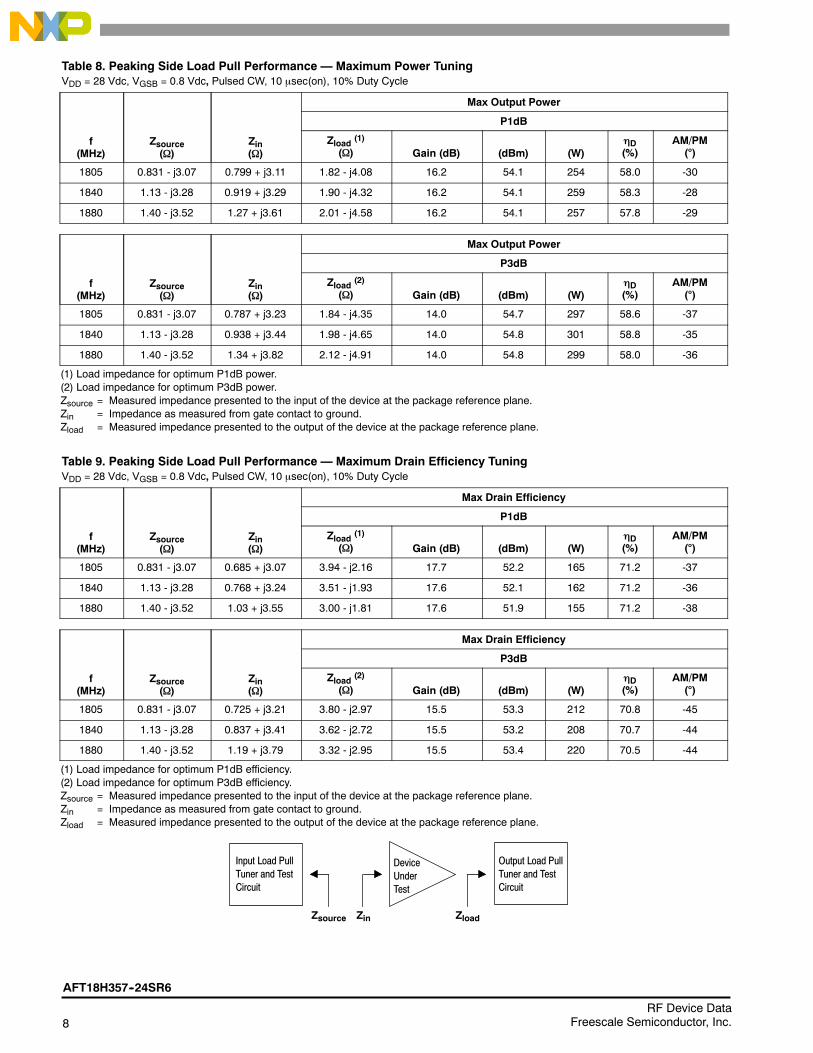
Table 8. Peaking Side Load Pull Performance — Maximum Power TuningVDD = 28 Vdc, VGSB = 0.8 Vdc, Pulsed CW, 10 sec(on), 10% Duty Cycle
f(MHz)
Zsource()
Zin()
Max Output Power
P1dB
Zload (1)
() Gain (dB) (dBm) (W)D(%)
AM/PM()
1805 0.831 - j3.07 0.799 + j3.11 1.82 - j4.08 16.2 54.1 254 58.0 -30
1840 1.13 - j3.28 0.919 + j3.29 1.90 - j4.32 16.2 54.1 259 58.3 -28
1880 1.40 - j3.52 1.27 + j3.61 2.01 - j4.58 16.2 54.1 257 57.8 -29
f(MHz)
Zsource()
Zin()
Max Output Power
P3dB
Zload (2)
() Gain (dB) (dBm) (W)D(%)
AM/PM()
1805 0.831 - j3.07 0.787 + j3.23 1.84 - j4.35 14.0 54.7 297 58.6 -37
1840 1.13 - j3.28 0.938 + j3.44 1.98 - j4.65 14.0 54.8 301 58.8 -35
1880 1.40 - j3.52 1.34 + j3.82 2.12 - j4.91 14.0 54.8 299 58.0 -36
(1) Load impedance for optimum P1dB power.(2) Load impedance for optimum P3dB power.Zsource = Measured impedance presented to the input of the device at the package reference plane.Zin = Impedance as measured from gate contact to ground.Zload = Measured impedance presented to the output of the device at the package reference plane.
Table 9. Peaking Side Load Pull Performance — Maximum Drain Efficiency TuningVDD = 28 Vdc, VGSB = 0.8 Vdc, Pulsed CW, 10 sec(on), 10% Duty Cycle
f(MHz)
Zsource()
Zin()
Max Drain Efficiency
P1dB
Zload (1)
() Gain (dB) (dBm) (W)D(%)
AM/PM()
1805 0.831 - j3.07 0.685 + j3.07 3.94 - j2.16 17.7 52.2 165 71.2 -37
1840 1.13 - j3.28 0.768 + j3.24 3.51 - j1.93 17.6 52.1 162 71.2 -36
1880 1.40 - j3.52 1.03 + j3.55 3.00 - j1.81 17.6 51.9 155 71.2 -38
f(MHz)
Zsource()
Zin()
Max Drain Efficiency
P3dB
Zload (2)
() Gain (dB) (dBm) (W)D(%)
AM/PM()
1805 0.831 - j3.07 0.725 + j3.21 3.80 - j2.97 15.5 53.3 212 70.8 -45
1840 1.13 - j3.28 0.837 + j3.41 3.62 - j2.72 15.5 53.2 208 70.7 -44
1880 1.40 - j3.52 1.19 + j3.79 3.32 - j2.95 15.5 53.4 220 70.5 -44
(1) Load impedance for optimum P1dB efficiency.(2) Load impedance for optimum P3dB efficiency.Zsource = Measured impedance presented to the input of the device at the package reference plane.Zin = Impedance as measured from gate contact to ground.Zload = Measured impedance presented to the output of the device at the package reference plane.
Input Load PullTuner and TestCircuit
DeviceUnderTest
Zsource Zin Zload
Output Load PullTuner and TestCircuit

AFT18H357--24SR6
9RF Device DataFreescale Semiconductor, Inc.
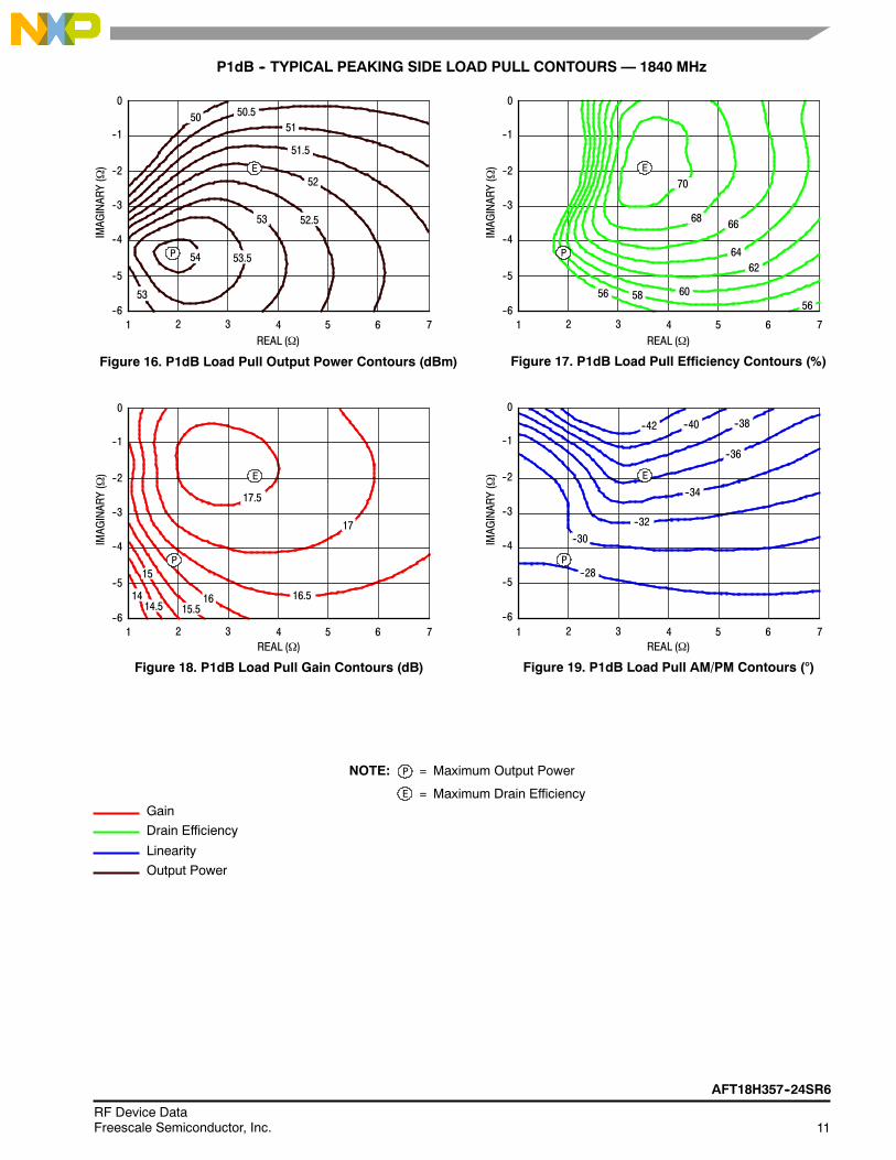
P1dB -- TYPICAL CARRIER SIDE LOAD PULL CONTOURS — 1840 MHz
--7
--1
--2
IMAGINARY()
2 2.51 6
--3
4.51.5
--4
--5
3.5 43
--6
5 5.5--7
--1
--2
IMAGINARY()
2 2.51 6
--3
4.51.5
--4
--5
3.5 43
--6
5 5.5
--7
--1
--2
IMAGINARY()
2 2.51 6
--3
4.51.5
--4
--5
3.5 43
--6
5 5.5
NOTE: = Maximum Output Power
= Maximum Drain Efficiency
P
E
Gain
Drain Efficiency
Linearity
Output Power
Figure 8. P1dB Load Pull Output Power Contours (dBm)
REAL ()
--7
--1
--2
IMAGINARY()
2 2.51 6
--3
4.51.5
Figure 9. P1dB Load Pull Efficiency Contours (%)
REAL ()
Figure 10. P1dB Load Pull Gain Contours (dB)
REAL ()
--4
--5
3.5 43
--6
5 5.5
Figure 11. P1dB Load Pull AM/PM Contours ()
REAL ()
E
P
48.5
48
4949.5
5050.55151.5
6058
565452
E
P
6264
66
P
E
19.5 20
20.5
21
21.5
2222.5
23
E
P--12
--16
--18
--20--24
--8
--10
--14
--22
68

10RF Device Data
Freescale Semiconductor, Inc.
AFT18H357--24SR6
P3dB -- TYPICAL CARRIER SIDE LOAD PULL CONTOURS — 1840 MHz
--7
--1
--2
IMAGINARY()
2 2.51 6
--3
4.51.5
--4
--5
3.5 43
--6
5 5.5--7
--1
--2
IMAGINARY()
2 2.51 6
--3
4.51.5
--4
--5
3.5 43
--6
5 5.5
--7
--1
--2
IMAGINARY()
2 2.51 6
--3
4.51.5
--4
--5
3.5 43
--6
5 5.5
NOTE: = Maximum Output Power
= Maximum Drain Efficiency
P
E
Gain
Drain Efficiency
Linearity
Output Power
Figure 12. P3dB Load Pull Output Power Contours (dBm)
REAL ()
--7
--1
--2
IMAGINARY()
2 2.51 6
--3
4.51.5
Figure 13. P3dB Load Pull Efficiency Contours (%)
REAL ()
Figure 14. P3dB Load Pull Gain Contours (dB)
REAL ()
--4
--5
3.5 43
--6
5 5.5
Figure 15. P3dB Load Pull AM/PM Contours ()
REAL ()
E
P
48.5
49
49.550
50.551
51.552
52.5
6058
5452
62
E
P
56
64
66
68
P
E
17
17.5 18
18.519
19.5
20
20.5
21
E
P
--14--16
--18
--20
--24
--26
--22
--28--30
AFT18H357--24SR6
11RF Device DataFreescale Semiconductor, Inc.
P1dB -- TYPICAL PEAKING SIDE LOAD PULL CONTOURS — 1840 MHz
NOTE: = Maximum Output Power
= Maximum Drain Efficiency
P
E
Gain
Drain Efficiency
Linearity
Output Power
Figure 16. P1dB Load Pull Output Power Contours (dBm)
REAL ()
IMAGINARY()
21 7
Figure 17. P1dB Load Pull Efficiency Contours (%)
REAL ()
Figure 18. P1dB Load Pull Gain Contours (dB)
REAL ()
43 5
Figure 19. P1dB Load Pull AM/PM Contours ()
REAL ()
605856
E
P
6264
66
6--6
--1
--2
IMAGINARY()
21 7
--3
--4
--5
43 5 6
IMAGINARY()
IMAGINARY()
21 743 5 6
0
--6
--1
--2
--3
--4
--5
0
E
P
50 50.551
51.5
52
52.553
53.554
68
70
56
21 743 5 6--6
--1
--2
--3
--4
--5
0
P
E
14.514
15
15.516 16.5
17
17.5
--6
--1
--2
--3
--4
--5
0
E
P
--32
--36
--38--42
--30
--34
--40
--28
53

12RF Device Data
Freescale Semiconductor, Inc.
AFT18H357--24SR6
P3dB -- TYPICAL PEAKING SIDE LOAD PULL CONTOURS — 1840 MHz
NOTE: = Maximum Output Power
= Maximum Drain Efficiency
P
E
Gain
Drain Efficiency
Linearity
Output Power
Figure 20. P3dB Load Pull Output Power Contours (dBm)
REAL ()
IMAGINARY()
21 7
Figure 21. P3dB Load Pull Efficiency Contours (%)
REAL ()
Figure 22. P3dB Load Pull Gain Contours (dB)
REAL ()
43 5
Figure 23. P3dB Load Pull AM/PM Contours ()
REAL ()
6--6
--1
--2
IMAGINARY()
21 7
--3
--4
--5
43 5 6
IMAGINARY()
IMAGINARY()
21 743 5 6
0
--6
--1
--2
--3
--4
--5
0
21 743 5 6--6
--1
--2
--3
--4
--5
0
--6
--1
--2
--3
--4
--5
0
6058
E
P
62
64
66
68
70E
P
5151.5
52
52.5
53
53.554
54.55654
P
E
14.5
15
15.5
12 1412.5
13
13.5
E
P
--32
--36
--38
--42
--34
--40
--44
--46--48
54
62
58

AFT18H357--24SR6
13RF Device DataFreescale Semiconductor, Inc.
ALTERNATE CHARACTERIZATION — 1930–1995 MHz
--
--
AFT18H357--24SRev. 6
D55813
VDDA
VDDB
VGGA
VGGB
C1
C
P
R1
C9
R2
C5
C17 C18
C6Z1
R3
C2
C10
C16
C14
C12
C8
C4
C19
C7
C3
C11C13
C15
Figure 24. AFT18H357--24SR6 Test Circuit Component Layout — 1930--1995 MHz
CUTOUTAREA
Table 10. AFT18H357--24SR6 Test Circuit Component Designations and Values — 1930--1995 MHzPart Description Part Number Manufacturer
C1, C2, C3, C4 15 pF Chip Capacitors ATC600F150JT250XT ATC
C5, C6, C8 8.2 pF Chip Capacitors ATC600F8R2JT250XT ATC
C7 3.9 pF Chip Capacitor ATC600F3R9JT250XT ATC
C9, C10, C11, C12,C13, C14
10 F Chip Capacitors C5750X7SA106K230KB TDK
C15, C16 220 F, 63 V Electrolytic Capacitors SK063M0220B5S-1015 YAGEO
C17, C19 0.2 pF Chip Capacitors ATC600F0R2BT250XT ATC
C18 0.9 pF Chip Capacitor ATC600F0R9BT250XT ATC
R1, R2 2.2 , 1/4 W Chip Resistors CRCW12062R20JNEA Vishay
R3 50 , 10 W Chip Resistor CW12010T0050GBK ATC
Z1 1700--2000 MHz Band 90, 5 dB Directional Coupler X3C19P1--05S Anaren
PCB Rogers RO4350B, 0.020, r = 3.66 D55813 MTL

14RF Device Data
Freescale Semiconductor, Inc.
AFT18H357--24SR6
TYPICAL CHARACTERISTICS — 1930–1995 MHz
1880
ACPR
f, FREQUENCY (MHz)
Figure 25. Single--Carrier Output Peak--to--Average RatioCompression (PARC) Broadband Performance @ Pout = 63 Watts Avg.
--2.5
--2.1
--2.2
--2.3
--2.4
16.5
17.5
17.4
17.3
--40
51
50.5
50
49.5
--30
--32
--34
--36
D,DRAIN
EFFICIENCY(%)
D
Gps,POWER
GAIN(dB) 17.2
17.1
17
16.9
16.8
16.7
16.6
1900 1920 1940 1960 1980 2000 2020 2040
49
--38
--2.6
ACPR
(dBc)
PARC
Gps
1
ACPR
Pout, OUTPUT POWER (WATTS) AVG.
Figure 26. Single--Carrier W--CDMA Power Gain, DrainEfficiency and ACPR versus Output Power
--20
--30
10
22
0
60
50
40
30
20
D,DRAINEFFICIENCY(%)
D
Gps,POWER
GAIN(dB)
20
18
10 100 400
10
--70
ACPR
(dBc)
16
14
12
--10
--40
--50
--60
Figure 27. Broadband Frequency Response
8
20
f, FREQUENCY (MHz)
16
14
12
GAIN(dB)
18
10
1660 1750 1840 1930 2020 2110 2200 2290
Gain
1960 MHzVDD = 28 Vdc, IDQA = 800 mAVGSB = 0.4 VdcSingle--Carrier W--CDMA
1930 MHz
1995 MHz
Gps
1930 MHz
1995 MHz
1960 MHz1930 MHz
1960 MHz
1995 MHz
VDD = 28 VdcPin = 0 dBmIDQA = 800 mAVGSB = 0.4 Vdc
PARC(dB)
VDD = 28 Vdc, Pout = 63 W (Avg.) IDQA = 800 mAVGSB = 0.4 Vdc, Single--Carrier W--CDMA, 3.84 MHzChannel Bandwidth, Input Signal PAR = 9.9 dB@ 0.01% Probability on CCDF
3.84 MHz Channel BandwidthInput Signal PAR = 9.9 dB@ 0.01%= Probability on CCDF
AFT18H357--24SR6
15RF Device DataFreescale Semiconductor, Inc.
Table 11. Carrier Side Load Pull Performance — Maximum Power TuningVDD = 28 Vdc, IDQA = 790 mA, Pulsed CW, 10 sec(on), 10% Duty Cycle
f(MHz)
Zsource()
Zin()
Max Output Power
P1dB
Zload (1)
() Gain (dB) (dBm) (W)D(%)
AM/PM()
1930 2.31 - j4.08 2.36 + j4.20 1.63 - j4.80 19.5 51.7 149 55.4 -11
1960 2.73 - j4.53 2.83 + j4.49 1.63 - j4.87 19.4 51.7 149 55.2 -11
1995 3.52 - j4.43 3.64 + j4.64 1.72 - j5.06 19.5 51.6 146 54.0 -11
f(MHz)
Zsource()
Zin()
Max Output Power
P3dB
Zload (2)
() Gain (dB) (dBm) (W)D(%)
AM/PM()
1930 2.31 - j4.08 2.34 + j4.60 1.62 - j5.05 17.2 52.5 178 56.1 -16
1960 2.73 - j4.53 2.89 + j4.97 1.66 - j5.16 17.2 52.5 177 55.7 -17
1995 3.52 - j4.43 3.88 + j5.20 1.76 - j5.34 17.2 52.4 173 54.7 -16
(1) Load impedance for optimum P1dB power.(2) Load impedance for optimum P3dB power.Zsource = Measured impedance presented to the input of the device at the package reference plane.Zin = Impedance as measured from gate contact to ground.Zload = Measured impedance presented to the output of the device at the package reference plane.
Table 12. Carrier Side Load Pull Performance — Maximum Drain Efficiency TuningVDD = 28 Vdc, IDQA = 790 mA, Pulsed CW, 10 sec(on), 10% Duty Cycle
f(MHz)
Zsource()
Zin()
Max Drain Efficiency
P1dB
Zload (1)
() Gain (dB) (dBm) (W)D(%)
AM/PM()
1930 2.31 - j4.08 2.25 + j4.31 2.94 - j3.26 22.0 49.9 98 65.8 -16
1960 2.73 - j4.53 2.72 + j4.60 2.87 - j3.27 22.0 49.8 95 65.4 -17
1995 3.52 - j4.43 3.52 + j4.76 2.89 - j3.42 22.1 49.7 94 63.6 -15
f(MHz)
Zsource()
Zin()
Max Drain Efficiency
P3dB
Zload (2)
() Gain (dB) (dBm) (W)D(%)
AM/PM()
1930 2.31 - j4.08 2.15 + j4.68 2.61 - j3.08 20.0 50.5 112 66.1 -26
1960 2.73 - j4.53 2.68 + j5.07 2.58 - j3.15 20.0 50.5 111 65.7 -26
1995 3.52 - j4.43 3.62 + j5.39 2.37 - j3.33 20.0 50.6 114 64.8 -25
(1) Load impedance for optimum P1dB efficiency.(2) Load impedance for optimum P3dB efficiency.Zsource = Measured impedance presented to the input of the device at the package reference plane.Zin = Impedance as measured from gate contact to ground.Zload = Measured impedance presented to the output of the device at the package reference plane.
Input Load PullTuner and TestCircuit
DeviceUnderTest
Zsource Zin Zload
Output Load PullTuner and TestCircuit

16RF Device Data
Freescale Semiconductor, Inc.
AFT18H357--24SR6
Table 13. Peaking Side Load Pull Performance — Maximum Power TuningVDD = 28 Vdc, VGSB = 0.8 Vdc, Pulsed CW, 10 sec(on), 10% Duty Cycle
f(MHz)
Zsource()
Zin()
Max Output Power
P1dB
Zload (1)
() Gain (dB) (dBm) (W)D(%)
AM/PM()
1930 2.31 - j4.08 2.00 + j4.23 2.28 - j4.89 16.1 54.1 256 57.5 -30
1960 3.28 - j4.32 2.69 + j4.66 2.54 - j5.11 16.1 54.1 255 57.7 -30
1995 4.55 - j4.25 4.00 + j4.92 2.87 - j5.40 16.1 54.0 250 56.3 -30
f(MHz)
Zsource()
Zin()
Max Output Power
P3dB
Zload (2)
() Gain (dB) (dBm) (W)D(%)
AM/PM()
1930 2.31 - j4.08 2.23 + j4.52 2.54 - j5.29 13.9 54.7 297 57.6 -36
1960 3.28 - j4.32 3.08 + j4.97 2.79 - j5.46 13.9 54.7 296 57.5 -37
1995 4.55 - j4.25 4.73 + j5.11 3.20 - j5.65 14.0 54.6 291 57.0 -37
(1) Load impedance for optimum P1dB power.(2) Load impedance for optimum P3dB power.Zsource = Measured impedance presented to the input of the device at the package reference plane.Zin = Impedance as measured from gate contact to ground.Zload = Measured impedance presented to the output of the device at the package reference plane.
Table 14. Peaking Side Load Pull Performance — Maximum Drain Efficiency TuningVDD = 28 Vdc, VGSB = 0.8 Vdc, Pulsed CW, 10 sec(on), 10% Duty Cycle
f(MHz)
Zsource()
Zin()
Max Drain Efficiency
P1dB
Zload (1)
() Gain (dB) (dBm) (W)D(%)
AM/PM()
1930 2.31 - j4.08 1.66 + j4.17 2.85 - j2.12 17.5 52.1 162 70.7 -37
1960 3.28 - j4.32 2.17 + j4.63 2.67 - j1.93 17.3 51.7 149 70.6 -39
1995 4.55 - j4.25 3.29 + j5.06 2.76 - j2.21 17.4 51.9 157 69.8 -37
f(MHz)
Zsource()
Zin()
Max Drain Efficiency
P3dB
Zload (2)
() Gain (dB) (dBm) (W)D(%)
AM/PM()
1930 2.31 - j4.08 1.95 + j4.48 3.18 - j2.71 15.3 53.2 208 70.0 -45
1960 3.28 - j4.32 2.69 + j4.98 3.13 - j2.72 15.3 53.2 207 69.8 -45
1995 4.55 - j4.25 4.09 + j5.32 2.90 - j2.56 15.4 52.8 191 69.0 -47
(1) Load impedance for optimum P1dB efficiency.(2) Load impedance for optimum P3dB efficiency.Zsource = Measured impedance presented to the input of the device at the package reference plane.Zin = Impedance as measured from gate contact to ground.Zload = Measured impedance presented to the output of the device at the package reference plane.
Input Load PullTuner and TestCircuit
DeviceUnderTest
Zsource Zin Zload
Output Load PullTuner and TestCircuit

AFT18H357--24SR6
17RF Device DataFreescale Semiconductor, Inc.
P1dB -- TYPICAL CARRIER SIDE LOAD PULL CONTOURS — 1960 MHz
--7
--1
--2
IMAGINARY()
2 2.51 6
--3
4.51.5
--4
--5
3.5 43
--6
5 5.5--7
--1
--2
IMAGINARY()
2 2.51 6
--3
4.51.5
--4
--5
3.5 43
--6
5 5.5
--7
--1
--2
IMAGINARY()
2 2.51 6
--3
4.51.5
--4
--5
3.5 43
--6
5 5.5
NOTE: = Maximum Output Power
= Maximum Drain Efficiency
P
E
Gain
Drain Efficiency
Linearity
Output Power
Figure 28. P1dB Load Pull Output Power Contours (dBm)
REAL ()
--7
--1
--2
IMAGINARY()
2 2.51 6
--3
4.51.5
Figure 29. P1dB Load Pull Efficiency Contours (%)
REAL ()
Figure 30. P1dB Load Pull Gain Contours (dB)
REAL ()
--4
--5
3.5 43
--6
5 5.5
Figure 31. P1dB Load Pull AM/PM Contours ()
REAL ()
P
48
49.5
50
47.5
51
51.5
E
48.5
49
50.5
58
56
5452
E
P
6264
E
P--12
--16
--18--20
--24
--10
--14
--22
P
E
19.5
20 20.5
21 21.5
22
22.5
23
50
19
50
60

18RF Device Data
Freescale Semiconductor, Inc.
AFT18H357--24SR6
P3dB -- TYPICAL CARRIER SIDE LOAD PULL CONTOURS — 1960 MHz
--7
--1
--2
IMAGINARY()
2 2.51 6
--3
4.51.5
--4
--5
3.5 43
--6
5 5.5--7
--1
--2
IMAGINARY()
2 2.51 6
--3
4.51.5
--4
--5
3.5 43
--6
5 5.5
--7
--1
--2
IMAGINARY()
2 2.51 6
--3
4.51.5
--4
--5
3.5 43
--6
5 5.5
NOTE: = Maximum Output Power
= Maximum Drain Efficiency
P
E
Gain
Drain Efficiency
Linearity
Output Power
Figure 32. P3dB Load Pull Output Power Contours (dBm)
REAL ()
--7
--1
--2
IMAGINARY()
2 2.51 6
--3
4.51.5
Figure 33. P3dB Load Pull Efficiency Contours (%)
REAL ()
Figure 34. P3dB Load Pull Gain Contours (dB)
REAL ()
--4
--5
3.5 43
--6
5 5.5
Figure 35. P3dB Load Pull AM/PM Contours ()
REAL ()
E
P
48.5
4949.5
50
50.551
51.5
52 60 58
54
52
62
56
64
E
P
--14
--16
--18
--20
--24--26
--22
--28--30
17 17.5
1818.5
19
19.5
20
20.5
21
E
P
E
P
51 50

AFT18H357--24SR6
19RF Device DataFreescale Semiconductor, Inc.
P1dB -- TYPICAL PEAKING SIDE LOAD PULL CONTOURS — 1960 MHz
IMAGINARY()
IMAGINARY()
NOTE: = Maximum Output Power
= Maximum Drain Efficiency
P
E
Gain
Drain Efficiency
Linearity
Output Power
Figure 36. P1dB Load Pull Output Power Contours (dBm)
REAL ()
--8
0
--2
IMAGINARY()
21 7
--3
Figure 37. P1dB Load Pull Efficiency Contours (%)
REAL ()
Figure 38. P1dB Load Pull Gain Contours (dB)
REAL ()
--4
--5
43
--6
5
Figure 39. P1dB Load Pull AM/PM Contours ()
REAL ()
6
--1
--7
--8
0
--2
21 7
--3
--4
--5
43
--6
5 6
--1
--7
--8
0
--2
21 7
--3
--4
--5
43
--6
5 6
--1
--7
--8
0
--2
21 7
--3
--4
--5
43
--6
5 6
--1
--7
E
P
50 51
51.5E
50.5
P
E
P
E
52
52.5
53
53.5
5352
52.5
54
60
5856
54
62
6466
P
E
70
68
13.5 14 14.515
15.5
16
16.5
17
16
--28
--30
--32
--34
--36
--38
--40
--42
IMAGINARY()

20RF Device Data
Freescale Semiconductor, Inc.
AFT18H357--24SR6
P3dB -- TYPICAL PEAKING SIDE LOAD PULL CONTOURS — 1960 MHz
2 2.51 64.51.5 3.5 43 5 5.5--8
--1
--2
--3
--4
--5
--6
--7
2 2.51 64.51.5 3.5 43 5 5.5--8
--1
--2
--3
--4
--5
--6
--7
2 2.51 64.51.5 3.5 43 5 5.5--8
--1
--2
--3
--4
--5
--6
--7
2 2.51 64.51.5 3.5 43 5 5.5
IMAGINARY()
IMAGINARY()
NOTE: = Maximum Output Power
= Maximum Drain Efficiency
P
E
Gain
Drain Efficiency
Linearity
Output Power
Figure 40. P3dB Load Pull Output Power Contours (dBm)
REAL ()
--8
--1
--2
IMAGINARY() --3
Figure 41. P3dB Load Pull Efficiency Contours (%)
REAL ()
Figure 42. P3dB Load Pull Gain Contours (dB)
REAL ()
--4
--5
--6
Figure 43. P3dB Load Pull AM/PM Contours ()
REAL ()
--7
P
53
52
54.5
5151.5
E
53.5
54
50.552.5
6058
56
68
E
P
6264
66
54
E
P
--34
P
E
11.5 12 12.513
13.5
14
14.5
15
--36
--38
--40--42--44--46
--48
--50
IMAGINARY()
52.5
52.5 53 53.5

AFT18H357--24SR6
21RF Device DataFreescale Semiconductor, Inc.
PACKAGE DIMENSIONS

22RF Device Data
Freescale Semiconductor, Inc.
AFT18H357--24SR6

AFT18H357--24SR6
23RF Device DataFreescale Semiconductor, Inc.
PRODUCT DOCUMENTATION, SOFTWARE AND TOOLS
Refer to the following resources to aid your design process.
Application Notes
AN1955: Thermal Measurement Methodology of RF Power AmplifiersEngineering Bulletins
EB212: Using Data Sheet Impedances for RF LDMOS DevicesSoftware
Electromigration MTTF Calculator RF High Power Model .s2p FileDevelopment Tools
Printed Circuit Boards
For Software and Tools, do a Part Number search at http://www.freescale.com, and select the “Part Number” link. Go to theSoftware & Tools tab on the part’s Product Summary page to download the respective tool.
REVISION HISTORY
The following table summarizes revisions to this document.
Revision Date Description
0 Mar. 2014 Initial Release of Data Sheet

24RF Device Data
Freescale Semiconductor, Inc.
AFT18H357--24SR6
Information in this document is provided solely to enable system and softwareimplementers to use Freescale products. There are no express or implied copyrightlicenses granted hereunder to design or fabricate any integrated circuits based on theinformation in this document.
Freescale reserves the right to make changes without further notice to any productsherein. Freescale makes no warranty, representation, or guarantee regarding thesuitability of its products for any particular purpose, nor does Freescale assume anyliability arising out of the application or use of any product or circuit, and specificallydisclaims any and all liability, including without limitation consequential or incidentaldamages. “Typical” parameters that may be provided in Freescale data sheets and/orspecifications can and do vary in different applications, and actual performance mayvary over time. All operating parameters, including “typicals,” must be validated foreach customer application by customer’s technical experts. Freescale does not conveyany license under its patent rights nor the rights of others. Freescale sells productspursuant to standard terms and conditions of sale, which can be found at the followingaddress: freescale.com/SalesTermsandConditions.
Freescale and the Freescale logo are trademarks of Freescale Semiconductor, Inc.,Reg. U.S. Pat. & Tm. Off. Airfast is a trademark of Freescale Semiconductor, Inc. Allother product or service names are the property of their respective owners.E 2014 Freescale Semiconductor, Inc.
How to Reach Us:
Home Page:freescale.com
Web Support:freescale.com/support
Document Number: AFT18H357--24SRev. 0, 3/2014