RF Power LDMOS Transistor - NXP...
18
RF Power LDMOS Transistor N-Channel Enhancement-Mode Lateral MOSFET This 63 watt RF power LDMOS transistor is designed for cellular base station applications covering the frequency range of 1805 to 1995 MHz. • Typical Single-Carrier W-CDMA Performance: V DD = 28 Volts, I DQ = 2000 mA, P out = 63 Watts Avg., Input Signal PAR = 9.9 dB @ 0.01% Probability on CCDF. Frequency G ps (dB) h D (%) Output PAR (dB) ACPR (dBc) IRL (dB) 1930 MHz 18.0 31.2 7.1 -36.0 -19 1960 MHz 18.2 31.2 7.1 -35.0 -19 1995 MHz 18.2 31.8 6.9 -35.0 -12 1800 MHz • Typical Single-Carrier W-CDMA Performance: V DD = 28 Volts, I DQ = 2000 mA, P out = 63 Watts Avg., Input Signal PAR = 9.9 dB @ 0.01% Probability on CCDF. Frequency G ps (dB) h D (%) Output PAR (dB) ACPR (dBc) IRL (dB) 1805 MHz 18.0 33.3 7.1 -35.0 -13 1840 MHz 18.2 32.7 7.1 -35.0 -16 1880 MHz 18.3 32.6 7.1 -34.0 -13 Features • Greater Negative Gate-Source Voltage Range for Improved Class C Operation • Designed for Digital Predistortion Error Correction Systems • Optimized for Doherty Applications • In Tape and Reel. R3 Suffix = 250 Units, 44 mm Tape Width, 13-inch Reel. Document Number: AFT18S290-13S Rev. 0, 5/2013 Freescale Semiconductor Technical Data 1805-1995 MHz, 63 W AVG., 28 V AFT18S290-13SR3 Figure 1. Pin Connections NI-880XS-2L4S (Top View) RF in /V GS VBW舂 (1) N.C. VBW舂 (1) 1 6 3 4 2 5 N.C. RF out /V DS 1. Device cannot operate with the V DD current supplied through pin 4 and pin 6. © Freescale Semiconductor, Inc., 2013. All rights reserved.
-
Upload
dangkhuong -
Category
Documents
-
view
219 -
download
0
Transcript of RF Power LDMOS Transistor - NXP...

AFT18S290−13SR3
1RF Device DataFreescale Semiconductor, Inc.
RF Power LDMOS TransistorN−Channel Enhancement−Mode Lateral MOSFET
This 63 watt RF power LDMOS transistor is designed for cellular base stationapplications covering the frequency range of 1805 to 1995 MHz.
• Typical Single−Carrier W−CDMA Performance: VDD = 28 Volts, IDQ = 2000 mA, Pout = 63 Watts Avg., Input Signal PAR = 9.9 dB @ 0.01%Probability on CCDF.
FrequencyGps(dB)
�D(%)
Output PAR(dB)
ACPR(dBc)
IRL(dB)
1930 MHz 18.0 31.2 7.1 −36.0 −19
1960 MHz 18.2 31.2 7.1 −35.0 −19
1995 MHz 18.2 31.8 6.9 −35.0 −12
1800 MHz• Typical Single−Carrier W−CDMA Performance: VDD = 28 Volts,
IDQ = 2000 mA, Pout = 63 Watts Avg., Input Signal PAR = 9.9 dB @ 0.01%Probability on CCDF.
FrequencyGps(dB)
�D(%)
Output PAR(dB)
ACPR(dBc)
IRL(dB)
1805 MHz 18.0 33.3 7.1 −35.0 −13
1840 MHz 18.2 32.7 7.1 −35.0 −16
1880 MHz 18.3 32.6 7.1 −34.0 −13
Features
• Greater Negative Gate−Source Voltage Range for Improved Class COperation
• Designed for Digital Predistortion Error Correction Systems• Optimized for Doherty Applications• In Tape and Reel. R3 Suffix = 250 Units, 44 mm Tape Width, 13−inch Reel.
Document Number: AFT18S290−13SRev. 0, 5/2013
Freescale SemiconductorTechnical Data
1805−1995 MHz, 63 W AVG., 28 V
AFT18S290−13SR3
Figure 1. Pin Connections
NI−880XS−2L4S
(Top View)
RFin/VGS
VBW�(1)N.C.
VBW�(1)
1 6
3 4
2 5
N.C.
RFout/VDS
1. Device cannot operate with the VDD currentsupplied through pin 4 and pin 6.
© Freescale Semiconductor, Inc., 2013. All rights reserved.

2RF Device Data
Freescale Semiconductor, Inc.
AFT18S290−13SR3
Table 1. Maximum Ratings
Rating Symbol Value Unit
Drain−Source Voltage VDSS −0.5, +65 Vdc
Gate−Source Voltage VGS −6.0, +10 Vdc
Operating Voltage VDD 32, +0 Vdc
Storage Temperature Range Tstg −65 to +150 °C
Case Operating Temperature Range TC −40 to +150 °C
Operating Junction Temperature Range (1,2) TJ −40 to +225 °C
CW Operation @ TC = 25°CDerate above 25°C
CW 2451.6
WW/°C
Table 2. Thermal Characteristics
Characteristic Symbol Value (2,3) Unit
Thermal Resistance, Junction to CaseCase Temperature 80°C, 66 W CW, 28 Vdc, IDQ = 2000 mA, 1960 MHz
RθJC 0.42 °C/W
Table 3. ESD Protection Characteristics
Test Methodology Class
Human Body Model (per JESD22−A114) 2
Machine Model (per EIA/JESD22−A115) B
Charge Device Model (per JESD22−C101) IV
Table 4. Electrical Characteristics (TA = 25°C unless otherwise noted)
Characteristic Symbol Min Typ Max Unit
Off Characteristics
Zero Gate Voltage Drain Leakage Current(VDS = 65 Vdc, VGS = 0 Vdc)
IDSS — — 10 μAdc
Zero Gate Voltage Drain Leakage Current(VDS = 28 Vdc, VGS = 0 Vdc)
IDSS — — 1 μAdc
Gate−Source Leakage Current(VGS = 5 Vdc, VDS = 0 Vdc)
IGSS — — 1 μAdc
On Characteristics
Gate Threshold Voltage(VDS = 10 Vdc, ID = 389 μAdc)
VGS(th) 1.5 2.0 2.5 Vdc
Gate Quiescent Voltage(VDD = 28 Vdc, ID = 2000 mAdc, Measured in Functional Test)
VGS(Q) 2.3 2.8 3.3 Vdc
Drain−Source On−Voltage(VGS = 10 Vdc, ID = 5.0 Adc)
VDS(on) 0.1 0.2 0.3 Vdc
1. Continuous use at maximum temperature will affect MTTF. 2. MTTF calculator available at http://www.freescale.com/rf. Select Software & Tools/Development Tools/Calculators to access MTTF
calculators by product. 3. Refer to AN1955, Thermal Measurement Methodology of RF Power Amplifiers. Go to http://www.freescale.com/rf. Select
Documentation/Application Notes − AN1955.
(continued)

AFT18S290−13SR3
3RF Device DataFreescale Semiconductor, Inc.
Table 4. Electrical Characteristics (TA = 25°C unless otherwise noted) (continued)
Characteristic Symbol Min Typ Max Unit
Functional Tests (1) (In Freescale Test Fixture, 50 ohm system) VDD = 28 Vdc, IDQ = 2000 mA, Pout = 63 W Avg., f = 1960 MHz,Single−Carrier W−CDMA, IQ Magnitude Clipping, Input Signal PAR = 9.9 dB @ 0.01% Probability on CCDF. ACPR measured in 3.84 MHzChannel Bandwidth @ ±5 MHz Offset.
Power Gain Gps 17.2 18.2 20.2 dB
Drain Efficiency ηD 29.5 31.2 — %
Output Peak−to−Average Ratio @ 0.01% Probability on CCDF PAR 6.6 7.1 — dB
Adjacent Channel Power Ratio ACPR — −35.0 −34.0 dBc
Input Return Loss IRL — −19 −6 dB
Load Mismatch (In Freescale Test Fixture, 50 ohm system) IDQ = 2000 mA, f = 1960 MHz
VSWR 10:1 at 32 Vdc, 363 W CW (2) Output Power(3 dB Input Overdrive from 263 W CW (2) Rated Power)
No Device Degradation
Typical Performance (In Freescale Test Fixture, 50 ohm system) VDD = 28 Vdc, IDQ = 2000 mA, 1930−1995 MHz Bandwidth
Pout @ 1 dB Compression Point, CW P1dB — 263 (2) — W
AM/PM(Maximum value measured at the P3dB compression point acrossthe 1930−1995 MHz bandwidth)
Φ — 15 — °
VBW Resonance Point(IMD Third Order Intermodulation Inflection Point)
VBWres — 85 — MHz
Gain Flatness in 65 MHz Bandwidth @ Pout = 63 W Avg. GF — 0.2 — dB
Gain Variation over Temperature(−30°C to +85°C)
ΔG — 0.01 — dB/°C
Output Power Variation over Temperature(−30°C to +85°C) (2)
ΔP1dB — 0.003 — dB/°C
1. Part internally matched both on input and output. 2. Exceeds recommended operating conditions. See CW operation data in Maximum Ratings table.

4RF Device Data
Freescale Semiconductor, Inc.
AFT18S290−13SR3
Figure 2. AFT18S290−13SR3 Test Circuit Component Layout — 1930−1995 MHz
C1*
C2*
C4* C5*
C6*
C7
C8
C9*C10*
C11* C12* C13*
C14
C15
C16
C17
C18
C21
C19C20
C22C23
C24
C25
AFT18S290-13SRev. 0
CU
T O
UT
AREA
R1
R2
C3*
*C1, C2, C3, C4, C5, C6, C9, C10, C11, C12 and C13 are mounted vertically.
VGG
VGG
VDD
VDD
Table 5. AFT18S290−13SR3 Test Circuit Component Designations and Values — 1930−1995 MHz
Part Description Part Number Manufacturer
C1, C2, C3, C7 C8 8.2 pF Chip Capacitors ATC100B8R2BT500XT ATC
C4 0.8 pF Chip Capacitor ATC100B0R8BT500XT ATC
C5 1.1 pF Chip Capacitor ATC100B1R1BT500XT ATC
C6 0.7 pF Chip Capacitor ATC100B0R7BT500XT ATC
C9, C10 8.2 pF Chip Capacitors ATC800B8R2BT500XT ATC
C11, C12 0.4 pF Chip Capacitors ATC100B0R4BT500XT ATC
C13 0.5 pF Chip Capacitor ATC100B0R5BT500XT ATC
C14, C15, C16, C17, C18, C19, C20,C21, C22, C23
10 μF Chip Capacitors C5750X7S2A106M230KB TDK
C24, C25 470 μF, 63 V Electrolytic Capacitors UVZ1J471MHD Nichicon
R1, R2 2 Ω, 1/4 W Chip Resistors CRCW12062R00FKEA Vishay
PCB 0.020�, �r = 3.5 RO4350B Rogers
AFT18S290−13SR3
5RF Device DataFreescale Semiconductor, Inc.
TYPICAL CHARACTERISTICS — 1930−1995 MHz
IRL,
INPU
T R
ETU
RN
LO
SS (d
B)
1880
f, FREQUENCY (MHz)
-20
-4
-8
-12
-16
15.5
20.5
20
19.5
-35.5
33
32.5
32
31.5
-33
-33.5
-34
-34.5
η D, D
RAI
NEF
FIC
IEN
CY
(%)
Gps
, PO
WER
GAI
N (d
B) 19
18.5
18
17.5
17
16.5
16
1900 1920 1940 1960 1980 2000 2020 2040
31
-35
-24
ACPR
(dBc
)10
-60
-10
-20
-30
-50
1 100
IMD
, IN
TER
MO
DU
LATI
ON
DIS
TORT
ION
(dBc
)
-40IM5-U
IM5-L
IM7-L
IM7-U
VDD = 28 Vdc, Pout = 100 W (PEP), IDQ = 2000 mATwo-Tone Measurements, (f1 + f2)/2 = CenterFrequency of 1960 MHz
Pout, OUTPUT POWER (WATTS)
-1
-3
25
0
-2
-4
OU
TPU
T C
OM
PRES
SIO
N A
T 0.
01%
PRO
BABI
LITY
ON
CC
DF
(dB)
10 40 55 8510
40
35
30
25
20
15
η D, D
RAI
N E
FFIC
IEN
CY
(%)
-3 dB = 64 W
70
ηD
ACPR
ACPR
(dBc
)
-50
-20
-25
-30
-40
-35
-45
19
Gps
, PO
WER
GAI
N (d
B)
18.5
18
17.5
17
16.5
16
-1 dB = 34 W-2 dB = 47 W
PAR
C (d
B)
-3.5
-2.7
-2.9
-3.1
-3.3
-3.7
-5
1
Figure 3. Single−Carrier Output Peak−to−Average Ratio Compression(PARC) Broadband Performance @ Pout = 63 Watts Avg.
Figure 4. Intermodulation Distortion Productsversus Two−Tone Spacing
TWO-TONE SPACING (MHz)
Figure 5. Output Peak−to−Average RatioCompression (PARC) versus Output Power
VDD = 28 Vdc, IDQ = 2000 mA, f = 1960 MHzSingle-Carrier W-CDMA, 3.84 MHz Channel Bandwidth
IM3-L
IM3-U
Gps
Input Signal PAR = 9.9 dB @ 0.01% Probability on CCDF
PARC
ACPR
PARC
VDD = 28 Vdc, Pout = 63 W (Avg.), IDQ = 2000 mASingle-Carrier W-CDMA, 3.84 MHz Channel Bandwidth
IRL
Gps
Input Signal PAR = 9.9 dB @ 0.01% Probability on CCDF
ηD

6RF Device Data
Freescale Semiconductor, Inc.
AFT18S290−13SR3
TYPICAL CHARACTERISTICS — 1930−1995 MHz
1
ACPR
Pout, OUTPUT POWER (WATTS) AVG.
Figure 6. Single−Carrier W−CDMA Power Gain, DrainEfficiency and ACPR versus Output Power
-10
-20
15
21
0
60
50
40
30
20
η D, D
RAI
N E
FFIC
IEN
CY
(%)
Gps
, PO
WER
GAI
N (d
B)
20
19
10 100
10
-60
ACPR
(dBc
)
18
17
16
0
-30
-40
-50
Figure 7. Broadband Frequency Response
9
21
f, FREQUENCY (MHz)
VDD = 28 VdcPin = 0 dBmIDQ = 2000 mA
17
15
13
GAI
N (d
B)
19
11
1500 1600 1700 1800 1900 2000 2100 2200 2300-30
30
20
10
0
-10
IRL
(dB)
-20
Gain
IRL
1930 MHz1960 MHz Gps
ηD
1930 MHz
Input Signal PAR = 9.9 dB@ 0.01% Probability on CCDF
300
1995 MHz
1930 MHz 1995 MHz
1960 MHz1995 MHz
VDD = 28 Vdc, IDQ = 2000 mA, Single-Carrier W-CDMA3.84 MHz Channel Bandwidth
1960 MHz

AFT18S290−13SR3
7RF Device DataFreescale Semiconductor, Inc.
VDD = 28 Vdc, IDQ = 2077 mA, Pulsed CW, 10 μsec(on), 10% Duty Cycle
f(MHz)
Zsource(�)
Zin(�)
Max Output Power
P1dB
Zload (1)
(�) Gain (dB) (dBm) (W)�D(%)
AM/PM(�)
1930 4.65 − j5.42 4.26 + j5.36 1.01 − j2.59 17.2 55.4 344 53.8 −11
1960 5.36 − j4.16 6.21 + j4.97 1.07 − j2.68 17.2 55.2 334 53.5 −10
1990 8.71 − j2.52 8.15 + j2.81 1.09 − j2.82 17.2 55.3 338 53.1 −11
f(MHz)
Zsource(�)
Zin(�)
Max Output Power
P3dB
Zload (2)
(�) Gain (dB) (dBm) (W)�D(%)
AM/PM(�)
1930 4.65 − j5.42 4.49 + j5.53 1.07 − j2.75 15.0 56.2 419 57.1 −15
1960 5.36 − j4.16 6.63 + j5.03 1.11 − j2.85 15.0 56.1 407 55.9 −15
1990 8.71 − j2.52 8.59 + j2.49 1.16 − j2.99 15.0 56.1 411 55.8 −16
(1) Load impedance for optimum P1dB power.(2) Load impedance for optimum P3dB power.Zsource = Measured impedance presented to the input of the device at the package reference plane.Zin = Impedance as measured from gate contact to ground.Zload = Measured impedance presented to the output of the device at the package reference plane.
Figure 8. Load Pull Performance — Maximum Power Tuning
VDD = 28 Vdc, IDQ = 2077 mA, Pulsed CW, 10 μsec(on), 10% Duty Cycle
f(MHz)
Zsource(�)
Zin(�)
Max Drain Efficiency
P1dB
Zload (1)
(�) Gain (dB) (dBm) (W)�D(%)
AM/PM(�)
1930 4.65 − j5.42 4.89 + j5.31 1.71 − j1.45 19.7 53.5 224 65.3 −16
1960 5.36 − j4.16 6.97 + j4.39 1.64 − j1.37 19.7 53.1 205 64.5 −15
1990 8.71 − j2.52 8.27 + j1.78 1.57 − j1.60 19.6 53.4 220 64.0 −16
f(MHz)
Zsource(�)
Zin(�)
Max Drain Efficiency
P3dB
Zload (2)
(�) Gain (dB) (dBm) (W)�D(%)
AM/PM(�)
1930 4.65 − j5.42 5.07 + j5.44 1.72 − j1.56 17.6 54.4 275 67.3 −23
1960 5.36 − j4.16 7.25 + j4.47 1.64 − j1.65 17.4 54.4 275 66.3 −22
1990 8.71 − j2.52 8.62 + j1.34 1.51 − j1.63 17.6 54.2 262 65.9 −24
(1) Load impedance for optimum P1dB efficiency.(2) Load impedance for optimum P3dB efficiency.Zsource = Measured impedance presented to the input of the device at the package reference plane.Zin = Impedance as measured from gate contact to ground.Zload = Measured impedance presented to the output of the device at the package reference plane.
Figure 9. Load Pull Performance — Maximum Drain Efficiency Tuning
Input Load PullTuner and TestCircuit
DeviceUnderTest
Zsource Zin Zload
Output Load PullTuner and TestCircuit
8RF Device Data
Freescale Semiconductor, Inc.
AFT18S290−13SR3
P1dB − TYPICAL LOAD PULL CONTOURS — 1960 MHz
-4
-1.5
-2.5
-3
-3.5
-2
1 1.5 2 2.5 30.5 3.5
-1
-0.5
-4
-1.5
-2.5
-3
-3.5
-2
1 1.5 2 2.5 30.5 3.5
-1
-0.5
Figure 10. P1dB Load Pull Output Power Contours (dBm)
-4
-1.5
REAL (Ω)
-2.5
-3
-3.5
IMAG
INAR
Y (Ω
)
-2
1 1.5 2 2.5 30.5 3.5
Figure 11. P1dB Load Pull Efficiency Contours (%)
REAL (Ω)
IMAG
INAR
Y (Ω
)
Figure 12. P1dB Load Pull Gain Contours (dB)
REAL (Ω)
IMAG
INAR
Y (Ω
)
Figure 13. P1dB Load Pull AM/PM Contours (�)
REAL (Ω)
IMAG
INAR
Y (Ω
)
NOTE: = Maximum Output Power
= Maximum Drain Efficiency
P
E
Power Gain
Drain Efficiency
Linearity
Output Power
-1
-0.551.5
51 52
53
54
55
52.5
53.5
54.5
P
E
54
-4
-1.5
-2.5
-3
-3.5
-2
1 1.5 2 2.5 30.5 3.5
-1
-0.5
545250
48
5658
60
62
64
P
E
19.5
18
18.5
20.5
17.5
16.5
17
19
20
P
E
-18
-20
-22
-24 -16
-14
-12
-10P
E
-8

AFT18S290−13SR3
9RF Device DataFreescale Semiconductor, Inc.
P3dB − TYPICAL LOAD PULL CONTOURS — 1960 MHz
IMAG
INAR
Y (Ω
)
IMAG
INAR
Y (Ω
)
NOTE: = Maximum Output Power
= Maximum Drain Efficiency
P
E
Power Gain
Drain Efficiency
Linearity
Output Power
-4
-1.5
-2.5
-3
-3.5
-2
1 1.5 2 2.5 30.5 3.5
-1
-0.5
-4
-1.5
-2.5
-3
-3.5
-2
15.5
1 1.5 2 2.5 30.5 3.5
18
18.5
14.5
17.5
-1
-0.5
16.5
17
16
15
P
E
P
E
-18-20-22-24
-16
-14
-12
-26-28
P
E
Figure 14. P3dB Load Pull Output Power Contours (dBm)
REAL (Ω)
IMAG
INAR
Y (Ω
)
-4
-1.5
-2.5
-3
-3.5
-2
1 1.5 2 2.5 30.5 3.5
-1
-0.5 52.5
5253
54
56
53.5
54.5
55.555
55P
E
-4
-1.5
-2.5
-3
-3.5
-2
1 1.5 2 2.5 30.5 3.5
-1
-0.5
Figure 15. P3dB Load Pull Efficiency Contours (%)
REAL (Ω)
IMAG
INAR
Y (Ω
)
545250
66
56
5860
62
64
Figure 16. P3dB Load Pull Gain Contours (dB)
REAL (Ω)
Figure 17. P3dB Load Pull AM/PM Contours (�)
REAL (Ω)

10RF Device Data
Freescale Semiconductor, Inc.
AFT18S290−13SR3
ALTERNATIVE CHARACTERIZATION — 1805−1880 MHz
Figure 18. AFT18S290−13SR3 Test Circuit Component Layout — 1805−1880 MHz
C1
C2
C4* C5*
C6
C7
C8
C9 R2
R1
C3*
C10*
C11*
C12*C13*
C14*
C15*
C16
C17
C18
C19
C20
C21
C23
C22
AFT18S290-13SRev. 0
CU
T O
UT
AREA
*C3, C4, C5, C10, C11, C12, C13, C14 and C15 are mounted vertically.
VGG
VGG
VDD
VDD
1805-1880 MHz
Table 6. AFT18S290−13SR3 Test Circuit Component Designations and Values — 1805−1880 MHz
Part Description Part Number Manufacturer
C1, C2, C10, C11 12 pF Chip Capacitors ATC100B120JT500XT ATC
C3 8.2 pF Chip Capacitor ATC100B8R2CT500XT ATC
C4 0.7 pF Chip Capacitor ATC100B0R7BT500XT ATC
C5 0.8 pF Chip Capacitor ATC100B0R8BT500XT ATC
C6, C7, C8, C9 10 μF Chip Capacitors GRM31CR61H106KA12L Murata
C12, C13 8.2 pF Chip Capacitors ATC800B8R2BW500XT ATC
C14, C15 0.4 pF Chip Capacitors ATC100B0R4BT500XT ATC
C16, C17, C18, C19, C20, C21 10 μF Chip Capacitors C5750X7S2A106M230KB TDK
C22, C23 470 μF, 63 V Electrolytic Capacitors MCGPR63V477M13X26−RH Multicomp
R1, R2 2 Ω, 1/4 W Chip Resistors CRCW12062R00FKEA Vishay
PCB 0.020�, �r = 3.5 RO4350B Rogers
AFT18S290−13SR3
11RF Device DataFreescale Semiconductor, Inc.
ALTERNATIVE CHARACTERIZATION — 1805−1880 MHz
IRL,
INPU
T R
ETU
RN
LO
SS (d
B)
1760
ACPR
f, FREQUENCY (MHz)
-16
-8
-10
-12
-14
15
20
19.5
19
-35
35
34
33
32
-32.5
-33
-33.5
-34
η D, D
RAI
NEF
FIC
IEN
CY
(%)
Gps
, PO
WER
GAI
N (d
B) 18.5
18
17.5
17
16.5
16
15.5
1780 1800 1820 1840 1860 1880 1900 1920
31
-34.5
-18
ACPR
(dBc
)
PARC
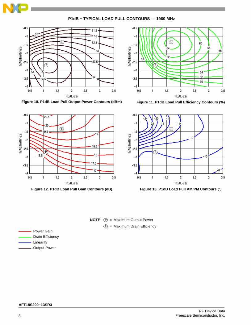
VDD = 28 Vdc, Pout = 63 W (Avg.), IDQ = 2000 mASingle-Carrier W-CDMA, 3.84 MHz Channel Bandwidth
IRL
PAR
C (d
B)
-3.2
-2.8
-2.9
-3
-3.1
-3.3
Gps
Input Signal PAR = 9.9 dB @0.01% Probability on CCDF
ηD
Figure 19. Single−Carrier Output Peak−to−Average Ratio Compression(PARC) Broadband Performance @ Pout = 63 Watts Avg.
1
ACPR
Pout, OUTPUT POWER (WATTS) AVG.
Figure 20. Single−Carrier W−CDMA Power Gain, DrainEfficiency and ACPR versus Output Power
-10
-20
15
21
0
60
50
40
30
20
η D, D
RAI
N E
FFIC
IEN
CY
(%)
Gps
, PO
WER
GAI
N (d
B)
20
19
10 100
10
-60
ACPR
(dBc
)
18
17
16
0
-30
-40
-50
Figure 21. Broadband Frequency Response
9
21
f, FREQUENCY (MHz)
VDD = 28 VdcPin = 0 dBmIDQ = 2000 mA
17
15
13
GAI
N (d
B)
19
11
1500 1600 1700 1800 1900 2000 2100 2200 2300-30
30
20
10
0
-10
IRL
(dB)
-20
Gain
IRL
Gps
ηD
300
VDD = 28 Vdc, IDQ = 2000 mA, Single-Carrier W-CDMA3.84 MHz Channel Bandwidth, Input Signal PAR = 9.9 dB@ 0.01% Probability on CCDF
1805 MHz 1840 MHz 1880 MHz
1880 MHz
1805 MHz1840 MHz
1880 MHz
1805 MHz1840 MHz

12RF Device Data
Freescale Semiconductor, Inc.
AFT18S290−13SR3
VDD = 28 Vdc, IDQ = 2078 mA, Pulsed CW, 10 μsec(on), 10% Duty Cycle
f(MHz)
Zsource(�)
Zin(�)
Max Output Power
P1dB
Zload (1)
(�) Gain (dB) (dBm) (W)�D(%)
AM/PM(�)
1800 1.17 − j3.88 1.11 + j3.95 1.04 − j2.20 17.5 55.1 325 52.8 −9.8
1840 1.50 − j4.53 1.55 + j4.38 1.01 − j2.27 17.4 55.3 339 53.9 −11
1880 2.48 − j5.08 2.36 + j4.86 1.02 − j2.51 17.3 55.3 341 54.2 −11
f(MHz)
Zsource(�)
Zin(�)
Max Output Power
P3dB
Zload (2)
(�) Gain (dB) (dBm) (W)�D(%)
AM/PM(�)
1800 1.17 − j3.88 1.10 + j4.01 1.03 − j2.36 15.3 56.1 405 57.0 −14
1840 1.50 − j4.53 1.56 + j4.47 1.03 − j2.53 15.1 56.2 417 57.3 −15
1880 2.48 − j5.08 2.39 + j5.03 1.02 − j2.62 15.1 56.2 418 57.0 −15
(1) Load impedance for optimum P1dB power.(2) Load impedance for optimum P3dB power.Zsource = Measured impedance presented to the input of the device at the package reference plane.Zin = Impedance as measured from gate contact to ground.Zload = Measured impedance presented to the output of the device at the package reference plane.
Figure 22. Load Pull Performance — Maximum Power Tuning
VDD = 28 Vdc, IDQ = 2078 mA, Pulsed CW, 10 μsec(on), 10% Duty Cycle
f(MHz)
Zsource(�)
Zin(�)
Max Drain Efficiency
P1dB
Zload (1)
(�) Gain (dB) (dBm) (W)�D(%)
AM/PM(�)
1800 1.17 − j3.88 1.26 + j4.14 2.57 − j1.57 20.0 53.2 210 64.5 −13
1840 1.50 − j4.53 1.76 + j4.52 2.26 − j1.49 19.8 53.4 220 64.7 −14
1880 2.48 − j5.08 2.70 + j4.93 2.21 − j1.55 19.7 53.4 218 65.1 −14
f(MHz)
Zsource(�)
Zin(�)
Max Drain Efficiency
P3dB
Zload (2)
(�) Gain (dB) (dBm) (W)�D(%)
AM/PM(�)
1800 1.17 − j3.88 1.26 + j4.15 2.45 − j1.87 17.7 54.4 274 67.0 −19
1840 1.50 − j4.53 1.74 + j4.58 2.14 − j1.76 17.5 54.6 290 67.4 −21
1880 2.48 − j5.08 2.70 + j5.11 2.04 − j1.73 17.5 54.5 285 67.4 −21
(1) Load impedance for optimum P1dB efficiency.(2) Load impedance for optimum P3dB efficiency.Zsource = Measured impedance presented to the input of the device at the package reference plane.Zin = Impedance as measured from gate contact to ground.Zload = Measured impedance presented to the output of the device at the package reference plane.
Figure 23. Load Pull Performance — Maximum Drain Efficiency Tuning
Input Load PullTuner and TestCircuit
DeviceUnderTest
Zsource Zin Zload
Output Load PullTuner and TestCircuit

AFT18S290−13SR3
13RF Device DataFreescale Semiconductor, Inc.
P1dB − TYPICAL LOAD PULL CONTOURS — 1840 MHz
-4
-1.5
-2.5
-3
-3.5
-2
1 1.5 2 2.5 30.5 3.5
-1
-0.5
-4
-1.5
-2.5
-3
-3.5
-2
1 1.5 2 2.5 30.5 3.5
-1
-0.5
IMAG
INAR
Y (Ω
)
IMAG
INAR
Y (Ω
)
NOTE: = Maximum Output Power
= Maximum Drain Efficiency
P
E
Power Gain
Drain Efficiency
Linearity
Output Power
P
E
19.5
1818.5
20.5
17.516.5 17
19
20
P
E -16
-14
-12
-10
P
E
-18
-20
Figure 24. P1dB Load Pull Output Power Contours (dBm)
-4
-1.5
REAL (Ω)
-2.5
-3
-3.5
IMAG
INAR
Y (Ω
)
-2
1 1.5 2 2.5 30.5 3.5
-1
-0.5
P
E
51.5
5253
54
55
52.553.5
54.5
52
51 51.5
-4
-1.5
-2.5
-3
-3.5
-2
1 1.5 2 2.5 30.5 3.5
-1
-0.5
Figure 25. P1dB Load Pull Efficiency Contours (%)
REAL (Ω)
IMAG
INAR
Y (Ω
)
5452504856
58
60
62
64
Figure 26. P1dB Load Pull Gain Contours (dB)
REAL (Ω)
Figure 27. P1dB Load Pull AM/PM Contours (�)
REAL (Ω)

14RF Device Data
Freescale Semiconductor, Inc.
AFT18S290−13SR3
P3dB − TYPICAL LOAD PULL CONTOURS — 1840 MHzIM
AGIN
ARY
(Ω)
IMAG
INAR
Y (Ω
)
NOTE: = Maximum Output Power
= Maximum Drain Efficiency
P
E
Power Gain
Drain Efficiency
Linearity
Output Power
-4
-1.5
-2.5
-3
-3.5
-2
1 1.5 2 2.5 30.5 3.5
-1
-0.5
-4
-1.5
-2.5
-3
-3.5
-2
1 1.5 2 2.5 30.5 3.5
-1
-0.5
15.5
18
18.5
14.5
17.5
16.5
17
16
15
-18
-20
-22-24
-16
-14-12
-26-28
P
E
P
E
Figure 28. P3dB Load Pull Output Power Contours (dBm)
REAL (Ω)
IMAG
INAR
Y (Ω
)
-4
-1.5
-2.5
-3
-3.5
-2
1 1.5 2 2.5 30.5 3.5
-1
-0.5
P
E
54.5
55
54
53.5
52.553
56
55.5
52.552
-4
-1.5
-2.5
-3
-3.5
-2
1 1.5 2 2.5 30.5 3.5
-1
-0.5
Figure 29. P3dB Load Pull Efficiency Contours (%)
REAL (Ω)
IMAG
INAR
Y (Ω
)
545250
66
5658
60
62
64P
E
Figure 30. P3dB Load Pull Gain Contours (dB)
REAL (Ω)
Figure 31. P3dB Load Pull AM/PM Contours (�)
REAL (Ω)

AFT18S290−13SR3
15RF Device DataFreescale Semiconductor, Inc.
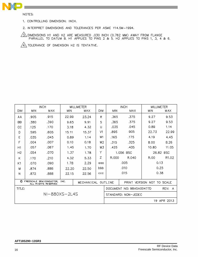
PACKAGE DIMENSIONS
16RF Device Data
Freescale Semiconductor, Inc.
AFT18S290−13SR3

AFT18S290−13SR3
17RF Device DataFreescale Semiconductor, Inc.
PRODUCT DOCUMENTATION, SOFTWARE AND TOOLS
Refer to the following documents, software and tools to aid your design process.
Application Notes• AN1955: Thermal Measurement Methodology of RF Power Amplifiers
Engineering Bulletins• EB212: Using Data Sheet Impedances for RF LDMOS Devices
Software• Electromigration MTTF Calculator
• RF High Power Model
• .s2p File
Development Tools• Printed Circuit Boards
For Software and Tools, do a Part Number search at http://www.freescale.com, and select the “Part Number” link. Go to theSoftware & Tools tab on the part’s Product Summary page to download the respective tool.
REVISION HISTORY
The following table summarizes revisions to this document.
Revision Date Description
0 May 2013 • Initial Release of Data Sheet

18RF Device Data
Freescale Semiconductor, Inc.
AFT18S290−13SR3
Information in this document is provided solely to enable system and softwareimplementers to use Freescale products. There are no express or implied copyrightlicenses granted hereunder to design or fabricate any integrated circuits based on theinformation in this document.
Freescale reserves the right to make changes without further notice to any productsherein. Freescale makes no warranty, representation, or guarantee regarding thesuitability of its products for any particular purpose, nor does Freescale assume anyliability arising out of the application or use of any product or circuit, and specificallydisclaims any and all liability, including without limitation consequential or incidentaldamages. “Typical” parameters that may be provided in Freescale data sheets and/orspecifications can and do vary in different applications, and actual performance mayvary over time. All operating parameters, including “typicals,” must be validated foreach customer application by customer’s technical experts. Freescale does not conveyany license under its patent rights nor the rights of others. Freescale sells productspursuant to standard terms and conditions of sale, which can be found at the followingaddress: freescale.com/SalesTermsandConditions.
Freescale and the Freescale logo are trademarks of Freescale Semiconductor, Inc.,Reg. U.S. Pat. & Tm. Off. Airfast is a trademark of Freescale Semiconductor, Inc. Allother product or service names are the property of their respective owners.� 2013 Freescale Semiconductor, Inc.
How to Reach Us:
Home Page:freescale.com
Web Support:freescale.com/support
Document Number: AFT18S290−13SRev. 0, 5/2013