Technical Data Rev. 3, 1/2010 RF LDMOS Wideband 2-Stage...
14
RF LDMOS Wideband 2-Stage Power Amplifiers Designed for broadband commercial and industrial applications with frequencies from 132 MHz to 960 MHz. The high gain and broadband performance of these devices make them ideal for large- signal, common- source amplifier applications in 28 volt base station equipment. These devices have a 2-stage design with off-chip matching for the input, interstage and output networks to cover the desired frequency band. • Typical Performance: 800 MHz, 28 Volts, I DQ1 = 80 mA, I DQ2 = 650 mA, P out = 70 Watts PEP Power Gain — 30 dB Drain Efficiency — 48% • Capable of Handling 10:1 VSWR, @ 28 Vdc, 850 MHz, 70 Watts CW Output Power Features • Characterized with Series Equivalent Large-Signal Impedance Parameters • Integrated Quiescent Current Temperature Compensation with Enable/Disable Function • On-Chip Current Mirror g m Reference FET for Self Biasing Application (1) • Integrated ESD Protection • 200°C Capable Plastic Package • RoHS Compliant • In Tape and Reel. R1 Suffix = 500 Units per 44 mm, 13 inch Reel. Figure 1. Functional Block Diagram Figure 2. Pin Connections V D1 /RF out1 RF in1 V RD2 V D2 /RF out2 Quiescent Current Temperature Compensation (1) V RG2 /V GS2 V RG1 /V GS1 V RD1 (Top View) GND GND RF in1 V D1 /RF out1 GND V RD2 V D2/ RF out2 GND V D1 /RF out1 GND V RG2 /V GS2 V RG1 /V GS1 V RD1 NC RF in2 NC 2 3 4 5 6 7 8 16 15 14 13 12 9 10 11 1 Note: Exposed backside flag is source terminal for transistors. V D1 /RF out1 RF in2 əɘ1. Refer to AN1977, Quiescent Current Thermal Tracking Circuit in the RF Integrated Circuit Family and to AN1987, Quiescent Current Control for the RF Integrated Circuit Device Family . Go to http://www.freescale.com/rf. Select Documentation/Application Notes - AN1977 or AN1987. Document Number: MW5IC970N Rev. 3, 1/2010 Freescale Semiconductor Technical Data 800-900 MHz, 70 W,ə28 V RF LDMOS WIDEBAND 2-ST AGE POWER AMPLIFIERS CASE 1329-09 TO-272 WB-16 PLASTIC MW5IC970NBR1 MW5IC970NBR1 MW5IC970GNBR1 CASE 1329A-04 TO-272 WB-16 GULL PLASTIC MW5IC970GNBR1 © Freescale Semiconductor, Inc., 2006, 2008, 2010. All rights reserved.
-
Upload
vuongtuyen -
Category
Documents
-
view
222 -
download
1
Transcript of Technical Data Rev. 3, 1/2010 RF LDMOS Wideband 2-Stage...

MW5IC970NBR1 MW5IC970GNBR1
1RF Device DataFreescale Semiconductor
RF LDMOS Wideband 2-Stage Power Amplifiers
Designed for broadband commercial and industrial applications withfrequencies from 132 MHz to 960 MHz. The high gain and broadbandperformance of these devices make them ideal for large- signal, common- sourceamplifier applications in 28 volt base station equipment. These devices have a2-stage design with off-chip matching for the input, interstage and outputnetworks to cover the desired frequency band.
• Typical Performance: 800 MHz, 28 Volts, IDQ1 = 80 mA, IDQ2 = 650 mA, Pout = 70 Watts PEP
Power Gain — 30 dBDrain Efficiency — 48%
• Capable of Handling 10:1 VSWR, @ 28 Vdc, 850 MHz, 70 Watts CW Output Power
Features• Characterized with Series Equivalent Large-Signal Impedance Parameters• Integrated Quiescent Current Temperature Compensation
with Enable/Disable Function• On-Chip Current Mirror gm Reference FET for Self Biasing Application (1)
• Integrated ESD Protection• 200°C Capable Plastic Package• RoHS Compliant• In Tape and Reel. R1 Suffix = 500 Units per 44 mm, 13 inch Reel.
Figure 1. Functional Block Diagram Figure 2. Pin Connections
VD1/RFout1
RFin1
VRD2
VD2/RFout2
Quiescent CurrentTemperature Compensation (1)
VRG2/VGS2
VRG1/VGS1
VRD1
(Top View)
GND
GND
RFin1
VD1/RFout1
GNDVRD2
VD2/RFout2
GND
VD1/RFout1
GND
VRG2/VGS2VRG1/VGS1
VRD1
NCRFin2
NC2345
6
78
1615
14
1312
91011
1
Note: Exposed backside flag is sourceterminal for transistors.
VD1/RFout1
RFin2
��1. Refer to AN1977, Quiescent Current Thermal Tracking Circuit in the RF Integrated Circuit Family and to AN1987, Quiescent Current Controlfor the RF Integrated Circuit Device Family. Go to http://www.freescale.com/rf. Select Documentation/Application Notes - AN1977 or AN1987.
Document Number: MW5IC970NRev. 3, 1/2010
Freescale SemiconductorTechnical Data
800-900 MHz, 70 W,�28 VRF LDMOS WIDEBAND
2-ST AGE POWER AMPLIFIERS
CASE 1329-09TO-272 WB-16
PLASTICMW5IC970NBR1
MW5IC970NBR1MW5IC970GNBR1
CASE 1329A-04TO-272 WB-16 GULL
PLASTICMW5IC970GNBR1
© Freescale Semiconductor, Inc., 2006, 2008, 2010. All rights reserved.
2RF Device Data
Freescale Semiconductor
MW5IC970NBR1 MW5IC970GNBR1
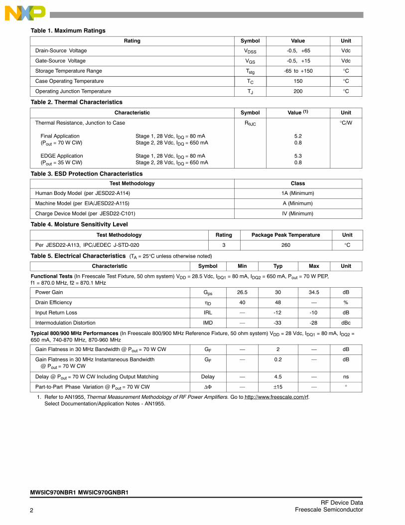
Table 1. Maximum Ratings
Rating Symbol Value Unit
Drain-Source Voltage VDSS -�0.5, +�65 Vdc
Gate-Source Voltage VGS -�0.5, +�15 Vdc
Storage Temperature Range Tstg -�65 to +150 °C
Case Operating Temperature TC 150 °C
Operating Junction Temperature TJ 200 °C
Table 2. Thermal Characteristics
Characteristic Symbol Value (1) Unit
Thermal Resistance, Junction to Case
Final Application Stage 1, 28 Vdc, IDQ = 80 mA(Pout = 70 W CW) Stage 2, 28 Vdc, IDQ = 650 mA
EDGE Application Stage 1, 28 Vdc, IDQ = 80 mA(Pout = 35 W CW) Stage 2, 28 Vdc, IDQ = 650 mA
RθJC
5.20.8
5.30.8
°C/W
Table 3. ESD Protection Characteristics
Test Methodology Class
Human Body Model (per JESD22-A114) 1A (Minimum)
Machine Model (per EIA/JESD22-A115) A (Minimum)
Charge Device Model (per JESD22-C101) IV (Minimum)
Table 4. Moisture Sensitivity Level
Test Methodology Rating Package Peak Temperature Unit
Per JESD22-A113, IPC/JEDEC J-STD-020 3 260 °C
Table 5. Electrical Characteristics (TA = 25°C unless otherwise noted)
Characteristic Symbol Min Typ Max Unit
Functional Tests (In Freescale Test Fixture, 50 ohm system) VDD = 28.5 Vdc, IDQ1 = 80 mA, IDQ2 = 650 mA, Pout = 70 W PEP, f1 = 870.0 MHz, f2 = 870.1 MHz
Power Gain Gps 26.5 30 34.5 dB
Drain Efficiency ηD 40 48 — %
Input Return Loss IRL — -12 -10 dB
Intermodulation Distortion IMD — -33 -28 dBc
Typical 800/900 MHz Performances (In Freescale 800/900 MHz Reference Fixture, 50 ohm system) VDD = 28 Vdc, IDQ1 = 80 mA, IDQ2 =650 mA, 740-870 MHz, 870-960 MHz
Gain Flatness in 30 MHz Bandwidth @ Pout = 70 W CW GF — 2 — dB
Gain Flatness in 30 MHz Instantaneous Bandwidth @ Pout = 70 W CW
GF — 0.2 — dB
Delay @ Pout = 70 W CW Including Output Matching Delay — 4.5 — ns
Part-to-Part Phase Variation @ Pout = 70 W CW ΔΦ — ±15 — °
��1. Refer to AN1955, Thermal Measurement Methodology of RF Power Amplifiers. Go to http://www.freescale.com/rf. Select Documentation/Application Notes - AN1955.
MW5IC970NBR1 MW5IC970GNBR1
3RF Device DataFreescale Semiconductor
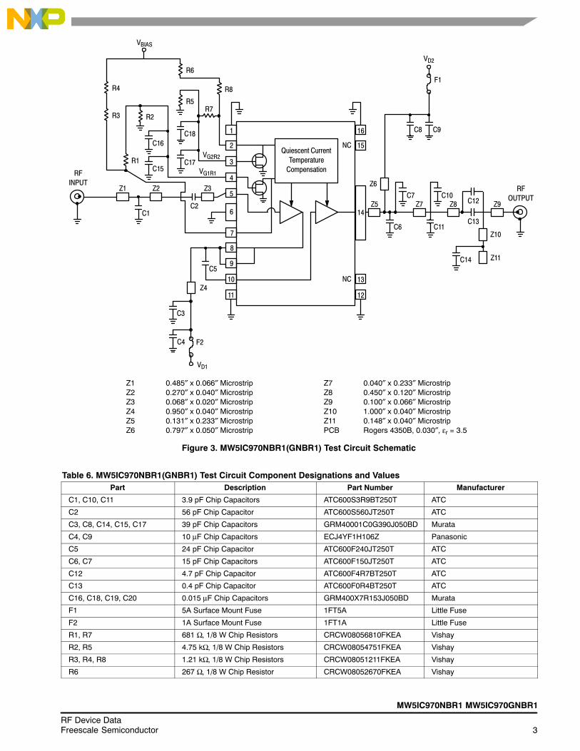
Figure 3. MW5IC970NBR1(GNBR1) Test Circuit Schematic
Z7 0.040″ x 0.233″ MicrostripZ8 0.450″ x 0.120″ MicrostripZ9 0.100″ x 0.066″ MicrostripZ10 1.000″ x 0.040″ MicrostripZ11 0.148″ x 0.040″ MicrostripPCB Rogers 4350B, 0.030″, εr = 3.5
Z1 0.485″ x 0.066″ MicrostripZ2 0.270″ x 0.040″ MicrostripZ3 0.068″ x 0.020″ MicrostripZ4 0.950″ x 0.040″ MicrostripZ5 0.131″ x 0.233″ MicrostripZ6 0.797″ x 0.050″ Microstrip
1 16
2
3
4
5
6
7
8
NC
14
15
12
13
11
10
9
NC
RFOUTPUT
C6
C7 C10
C11
Z5
Z6
Z7 Z8 C12
C13
Z10
C14 Z11
Z9
C8 C9
R8
C18
C17
R5R7
C15
C16
R2
R1
Z3
C2
R3
R4
RFINPUT
Z1 Z2
C1
R6
VBIAS
C5
Z4
C3
C4
VG1R1
VG2R2
VD1
F2
VD2
F1
Quiescent CurrentTemperature
Compensation
Table 6. MW5IC970NBR1(GNBR1) Test Circuit Component Designations and ValuesPart Description Part Number Manufacturer
C1, C10, C11 3.9 pF Chip Capacitors ATC600S3R9BT250T ATC
C2 56 pF Chip Capacitor ATC600S560JT250T ATC
C3, C8, C14, C15, C17 39 pF Chip Capacitors GRM40001C0G390J050BD Murata
C4, C9 10 μF Chip Capacitors ECJ4YF1H106Z Panasonic
C5 24 pF Chip Capacitor ATC600F240JT250T ATC
C6, C7 15 pF Chip Capacitors ATC600F150JT250T ATC
C12 4.7 pF Chip Capacitor ATC600F4R7BT250T ATC
C13 0.4 pF Chip Capacitor ATC600F0R4BT250T ATC
C16, C18, C19, C20 0.015 μF Chip Capacitors GRM400X7R153J050BD Murata
F1 5A Surface Mount Fuse 1FT5A Little Fuse
F2 1A Surface Mount Fuse 1FT1A Little Fuse
R1, R7 681 Ω, 1/8 W Chip Resistors CRCW08056810FKEA Vishay
R2, R5 4.75 kΩ, 1/8 W Chip Resistors CRCW08054751FKEA Vishay
R3, R4, R8 1.21 kΩ, 1/8 W Chip Resistors CRCW08051211FKEA Vishay
R6 267 Ω, 1/8 W Chip Resistor CRCW08052670FKEA Vishay

4RF Device Data
Freescale Semiconductor
MW5IC970NBR1 MW5IC970GNBR1
C
R6
MW5IC970
Rev. 1
VG2
VG1
R8
R7R4
R3
R1
R5
R2
C18C17
C16C15
C2
C5C1
C3
C4VD1
F2
VD2
F1
C9
C8
C7
C6
C11
C10
C12
C13
C14
Figure 4. MW5IC970NBR1(GNBR1) Test Circuit Component Layout

MW5IC970NBR1 MW5IC970GNBR1
5RF Device DataFreescale Semiconductor
TYPICAL CHARACTERISTICS
960-40
60
800-40
60
IRL
Gps
IMD
f, FREQUENCY (MHz)
VDD = 28.5 Vdc, Pout = 35 W (Avg.)IDQ1 = 80 mA, IDQ2 = 650 mA100 kHz Tone Spacing
40 40
20 20
0 0
-2 0 -20
840 880 920
Figure 5. Two-T one Wideband Performance @ Pout = 35 Watts (Avg.)
PAE
PA
E, P
OW
ER A
DD
ED E
FFIC
IEN
CY
(%)
Gps
, PO
WER
GAI
N (d
B)
IRL,
INPU
T R
ETU
RN
LO
SS (d
B)IM
D, I
NTE
RM
OD
ULA
TIO
N D
ISTO
RTIO
N (d
Bc)
Pout, OUTPUT POWER (WATTS) PEP
10027
32
1
IDQ2 = 975 mA
VDD = 28.5 Vdc, IDQ1 = 80 mAf1 = 870 MHz, f2 = 870.1 MHzTwo-Tone Measurements100 kHz Tone Spacing
31
30
28
10 200
Figure 6. Two-T one Power Gain versusOutput Power
Gps
, PO
WER
GAI
N (d
B)
300-70
-1 0
1
7th Order
VDD = 28.5 VdcIDQ1 = 80 mA, IDQ2 = 650 mAf1 = 870 MHz, f2 = 870.1 MHzTwo-Tone Measurements100 kHz Tone Spacing
5th Order
3rd Order
10
-2 0
-3 0
-4 0
-5 0
-6 0
Pout, OUTPUT POWER (WATTS) PEP
Figure 7. Intermodulation Distortion Productsversus Output Power
IMD
, IN
TER
MO
DU
LATI
ON
DIS
TORT
ION
(dBc
)
10-55
-2 0
0.1
7th Order
TWO-T ONE SPACING (MHz)
5th Order
3rd Order
-2 5
-3 0
-3 5
-4 0
-4 5
-5 0
1 200
Figure 8. Intermodulation Distortion Productsversus Tone Spacing
IMD
, IN
TER
MO
DU
LATI
ON
DIS
TORT
ION
(dBc
)
100020
34
0.10
70VDD = 28.5 Vdc, IDQ1 = 80 mAIDQ2 = 650 mA, f = 870 MHz
TC = 25�C
85�C
-30 �C
25�C85�C
101
32
30
28
26
24
22
60
50
40
30
20
10
Pout, OUTPUT POWER (WATTS) CW
Figure 9. Power Gain and Power AddedEfficiency versus CW Output Power
Gps
, PO
WER
GAI
N (d
B)
PAE,
PO
WER
AD
DED
EFF
ICIE
NC
Y (%
)
Gps
820 860 900 940
29
100
100
812 mA
650 mA
488 mA
325 mA
VDD = 28.5 Vdc, Pout = 35 W (PEP)IDQ1 = 80 mA, IDQ2 = 650 mATwo-Tone Measurements(f1 + f2)/2 = Center Frequency of 870 MHz
100
PAE
-30 �C

6RF Device Data
Freescale Semiconductor
MW5IC970NBR1 MW5IC970GNBR1
TYPICAL CHARACTERISTICS
Pout, OUTPUT POWER (WATTS) CW
Figure 10. Power Gain versus Output Power
16 V
IDQ1 = 80 mAIDQ2 = 650 mAf = 870 MHz
VDD = 12 V
10027
32
0 80
31
30
29
28
20 40 60
Gps
, PO
WER
GAI
N (d
B)
120 140
20 V24 V
28.5 V32 V

MW5IC970NBR1 MW5IC970GNBR1
7RF Device DataFreescale Semiconductor
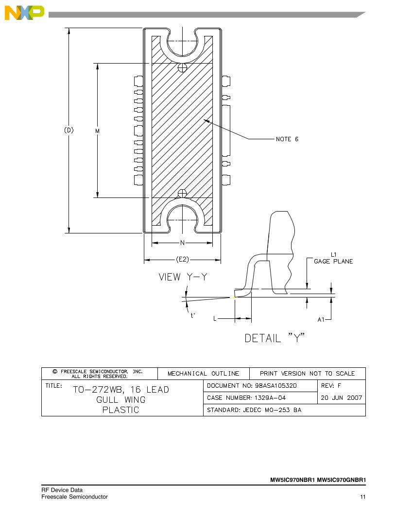
PACKAGE DIMENSIONS

8RF Device Data
Freescale Semiconductor
MW5IC970NBR1 MW5IC970GNBR1

MW5IC970NBR1 MW5IC970GNBR1
9RF Device DataFreescale Semiconductor
10RF Device Data
Freescale Semiconductor
MW5IC970NBR1 MW5IC970GNBR1
MW5IC970NBR1 MW5IC970GNBR1
11RF Device DataFreescale Semiconductor

12RF Device Data
Freescale Semiconductor
MW5IC970NBR1 MW5IC970GNBR1

MW5IC970NBR1 MW5IC970GNBR1
13RF Device DataFreescale Semiconductor
PRODUCT DOCUMENTATION
Refer to the following documents to aid your design process.
Application Notes
• AN1907: Solder Reflow Attach Method for High Power RF Devices in Plastic Packages
• AN1955: Thermal Measurement Methodology of RF Power Amplifiers
• AN1977: Quiescent Current Thermal Tracking Circuit in the RF Integrated Circuit Family
• AN1987: Quiescent Current Control for the RF Integrated Circuit Device Family
• AN3263: Bolt Down Mounting Method for High Power RF Transistors and RFICs in Over-Molded Plastic Packages
• AN3789: Clamping of High Power RF Transistors and RFICs in Over-Molded Plastic Packages
Engineering Bulletins• EB212: Using Data Sheet Impedances for RF LDMOS Devices
REVISION HISTORY
The following table summarizes revisions to this document.
Revision Date Description
2 Apr. 2008 • Document Number changed from MW5IC970NBR1 to MW5IC970N with the addition of theMW5IC970GNBR1 part number. Revision history sequencing maintained from first release of datasheet, p. 1
• Added Case Operating Temperature limit to the Maximum Ratings table and set limit to 150°C, p. 2
• Updated Part Numbers in Table 6, Component Designations and Values, to RoHS compliant partnumbers, p. 3
• Replaced Case Outline 1329-09, Issue L, with 1329-09, Issue M, p. 1, 7-9. Added pin numbers 1through 17.
• Added Case Outline 1329A-04, Issue F, p. 1, 10-12
• Added Product Documentation and Revision History, p. 13
3 Jan. 2010 • Changed Storage Temperature Range in Max Ratings table from -65 to +200 to -65 to +150 forstandardization across products, p. 2

14RF Device Data
Freescale Semiconductor
MW5IC970NBR1 MW5IC970GNBR1
Information in this document is provided solely to enable system and softwareimplementers to use Freescale Semiconductor products. There are no express orimplied copyright licenses granted hereunder to design or fabricate any integratedcircuits or integrated circuits based on the information in this document.
Freescale Semiconductor reserves the right to make changes without further notice toany products herein. Freescale Semiconductor makes no warranty, representation orguarantee regarding the suitability of its products for any particular purpose, nor doesFreescale Semiconductor assume any liability arising out of the application or use ofany product or circuit, and specifically disclaims any and all liability, including withoutlimitation consequential or incidental damages. “Typical” parameters that may beprovided in Freescale Semiconductor data sheets and/or specifications can and dovary in different applications and actual performance may vary over time. All operatingparameters, including “Typicals”, must be validated for each customer application bycustomer's technical experts. Freescale Semiconductor does not convey any licenseunder its patent rights nor the rights of others. Freescale Semiconductor products arenot designed, intended, or authorized for use as components in systems intended forsurgical implant into the body, or other applications intended to support or sustain life,or for any other application in which the failure of the Freescale Semiconductor productcould create a situation where personal injury or death may occur. Should Buyerpurchase or use Freescale Semiconductor products for any such unintended orunauthorized application, Buyer shall indemnify and hold Freescale Semiconductorand its officers, employees, subsidiaries, affiliates, and distributors harmless against allclaims, costs, damages, and expenses, and reasonable attorney fees arising out of,directly or indirectly, any claim of personal injury or death associated with suchunintended or unauthorized use, even if such claim alleges that FreescaleSemiconductor was negligent regarding the design or manufacture of the part.
Freescale� and the Freescale logo are trademarks of Freescale Semiconductor, Inc.All other product or service names are the property of their respective owners.© Freescale Semiconductor, Inc. 2006, 2008, 2010. All rights reserved.
How to Reach Us:
Home Page:www.freescale.com
Web Support:http://www.freescale.com/support
USA/Europe or Locations Not Listed:Freescale Semiconductor, Inc.Technical Information Center, EL5162100 East Elliot RoadTempe, Arizona 852841-800-521-6274 or +1-480-768-2130www.freescale.com/support
Europe, Middle East, and Africa:Freescale Halbleiter Deutschland GmbHTechnical Information CenterSchatzbogen 781829 Muenchen, Germany+44 1296 380 456 (English)+46 8 52200080 (English)+49 89 92103 559 (German)+33 1 69 35 48 48 (French)www.freescale.com/support
Japan:Freescale Semiconductor Japan Ltd.HeadquartersARCO Tower 15F1-8-1, Shimo-Meguro, Meguro-ku,Tokyo 153-0064Japan0120 191014 or +81 3 5437 [email protected]
Asia/Pacific:Freescale Semiconductor China Ltd.Exchange Building 23FNo. 118 Jianguo RoadChaoyang DistrictBeijing 100022 China +86 10 5879 [email protected]
For Literature Requests Only:Freescale Semiconductor Literature Distribution Center1-800-441-2447 or +1-303-675-2140Fax: [email protected]
Document Number: MW5IC970NRev. 3, 1/2010