Process Development for the Fabrication of Semiconductor ...
93
UNLV Theses, Dissertations, Professional Papers, and Capstones 12-1-2016 Process Development for the Fabrication of Semiconductor Process Development for the Fabrication of Semiconductor Devices and Circuits Using Spin-On Dopant Devices and Circuits Using Spin-On Dopant Richard R. Ryan University of Nevada, Las Vegas Follow this and additional works at: https://digitalscholarship.unlv.edu/thesesdissertations Part of the Electrical and Computer Engineering Commons, and the Science and Mathematics Education Commons Repository Citation Repository Citation Ryan, Richard R., "Process Development for the Fabrication of Semiconductor Devices and Circuits Using Spin-On Dopant" (2016). UNLV Theses, Dissertations, Professional Papers, and Capstones. 2898. http://dx.doi.org/10.34917/10083209 This Thesis is protected by copyright and/or related rights. It has been brought to you by Digital Scholarship@UNLV with permission from the rights-holder(s). You are free to use this Thesis in any way that is permitted by the copyright and related rights legislation that applies to your use. For other uses you need to obtain permission from the rights-holder(s) directly, unless additional rights are indicated by a Creative Commons license in the record and/ or on the work itself. This Thesis has been accepted for inclusion in UNLV Theses, Dissertations, Professional Papers, and Capstones by an authorized administrator of Digital Scholarship@UNLV. For more information, please contact [email protected].
Transcript of Process Development for the Fabrication of Semiconductor ...
UNLV Theses, Dissertations, Professional Papers, and Capstones
12-1-2016
Process Development for the Fabrication of Semiconductor Process Development for the Fabrication of Semiconductor
Devices and Circuits Using Spin-On Dopant Devices and Circuits Using Spin-On Dopant
Richard R. Ryan University of Nevada, Las Vegas
Follow this and additional works at: https://digitalscholarship.unlv.edu/thesesdissertations
Part of the Electrical and Computer Engineering Commons, and the Science and Mathematics
Education Commons
Repository Citation Repository Citation Ryan, Richard R., "Process Development for the Fabrication of Semiconductor Devices and Circuits Using Spin-On Dopant" (2016). UNLV Theses, Dissertations, Professional Papers, and Capstones. 2898. http://dx.doi.org/10.34917/10083209
This Thesis is protected by copyright and/or related rights. It has been brought to you by Digital Scholarship@UNLV with permission from the rights-holder(s). You are free to use this Thesis in any way that is permitted by the copyright and related rights legislation that applies to your use. For other uses you need to obtain permission from the rights-holder(s) directly, unless additional rights are indicated by a Creative Commons license in the record and/or on the work itself. This Thesis has been accepted for inclusion in UNLV Theses, Dissertations, Professional Papers, and Capstones by an authorized administrator of Digital Scholarship@UNLV. For more information, please contact [email protected].
PROCESS DEVELOPMENT FOR THE FABRICATION OF SEMICONDUCTOR DEVICES AND
CIRCUITS USING SPIN-ON DOPANT
By
Richard Robert Ryan
Bachelor of Science - Electrical Engineering
University of Nevada, Las Vegas
2012
A thesis submitted in partial fulfillment
of the requirements for the
Master of Science in Engineering - Electrical Engineering
Department of Electrical and Computer Engineering
Howard R. Hughes College of Engineering
The Graduate College
University of Nevada, Las Vegas
December 2016
ii
Thesis Approval
The Graduate College
The University of Nevada, Las Vegas
November 18, 2016
This thesis prepared by
Richard Robert Ryan
entitled
Process Development for the Fabrication of Semiconductor Devices and Circuits Using
Spin-On Dopant
is approved in partial fulfillment of the requirements for the degree of
Master of Science in Engineering – Electrical Engineering
Department of Electrical and Computer Engineering
Biswajit Das, Ph.D. Kathryn Hausbeck Korgan, Ph.D. Examination Committee Chair Graduate College Interim Dean
Yahia Baghzouz, Ph.D. Examination Committee Member
Yingtao Jiang, Ph.D. Examination Committee Member
Frank van Breukelen, Ph.D. Graduate College Faculty Representative
iii
Abstract
PROCESS DEVELOPMENT FOR THE FABRICATION OF SEMICONDUCTOR DEVICES AND
CIRCUITS USING SPIN-ON DOPANT
By
Richard R. Ryan
Department of Electrical Engineering
University of Nevada, Las Vegas
Traditional approaches to semiconductor device fabrication are expensive and time consuming,
making them out of reach for most universities and colleges. The objective of this thesis is to develop a
process by which semiconductor devices and circuits can be implemented completely in-house using
spin-on dopants (SODs), and low-cost transparency masks, to significantly reduce the lead time,
complexity, and cost associated with device fabrication. This will allow hands on fabrication experience
for students at universities and colleges without the traditional expensive device fabrication facilities. In
addition, it will also allow students and professors to design, fabricate and test semiconductor devices and
simple integrated circuits in house rapidly and inexpensively. The process developed in this project is
based on the existing facilities and equipment at the University of Nevada, Las Vegas; and can be
transferred to most university and college environments. A pn junction diode and a simple integrated
circuit consisting of pn junction diodes were used for the process development. The process was
optimized by comparing the effects of process variations, contact location, and diffusion heating profiles
on device characteristics. The process developed in this project is expected to provide hands-on
fabrication experience for students without such access, as well as for the rapid prototyping of simple
devices and integrated circuits for universities and colleges without expensive fabrication facilities.
.

iv
Table of Contents
Abstract ........................................................................................................................................................ iii
List of Tables ............................................................................................................................................... vi
List of Figures ............................................................................................................................................. vii
Chapter 1: Introduction ................................................................................................................................. 1
Section 1.1: Semiconductor Prototyping: ................................................................................................. 1
Section 1.2: Photolithography Masks: ...................................................................................................... 3
Section 1.3: Education: ............................................................................................................................. 3
Chapter 2: Background ................................................................................................................................. 6
Chapter 3: Experimental Design ................................................................................................................. 12
Section 3.1: Proof of Concept Experiment ............................................................................................. 12
Section 3.2: Mask Design and Fabrication ............................................................................................. 15
Section 3.3: Contact Comparison............................................................................................................ 19
Section 3.4: Diffusion Profile Variation ................................................................................................. 23
Section 3.5: Process Variation ................................................................................................................ 24
Chapter 4: Results and Analysis ................................................................................................................. 27
Section 4.1: Proof of Concept Analysis .................................................................................................. 27
Section 4.2: Contact Comparison............................................................................................................ 31
Section 4.3: Diffusion Profile Variation ................................................................................................. 34
Section 4.4: Process Variation ................................................................................................................ 38
Chapter 5: Conclusion ................................................................................................................................. 44
v
Appendix ..................................................................................................................................................... 48
A1: Cleaning Procedure .......................................................................................................................... 48
A2: Equipment Settings for Photoresist and Spin-On Dopant Spinning ................................................ 50
A3: Diffusion/Drive in Bake Furnace Controller Settings ...................................................................... 51
A4: Wafer Characterization and Doping Levels ..................................................................................... 52
A5: Specific Equipment, Symbols, and Constants ................................................................................. 53
A6: Minor and Major Flat Orientation to Determine Doping Type ........................................................ 54
A7: 4-Inch Wafer Results and Additional Materials............................................................................... 54
A8: Lab Procedures ................................................................................................................................. 55
Bibliography ............................................................................................................................................... 80
Curriculum Vitae ........................................................................................................................................ 82
vi
List of Tables
Table 1: The process to fabricate the Diffusion profile Comparison sample. ............................................. 24
Table 2: Overall experimental results ......................................................................................................... 42
Table 3: Piranha cleaning procedure ........................................................................................................... 48
Table 4: Buffered HF etchant preparation and wafer etching process. ....................................................... 50
Table 5: Spin coater parameters for PR1-1000A positive photoresist. ....................................................... 50
Table 6: Spin Coater parameters for P509 Spin-On dopant (SOD). ........................................................... 51
Table 7: Deep diffusion heating profile furnace settings ............................................................................ 51
Table 8: Short diffusion heating profile furnace settings ............................................................................ 52
Table 9: Silicon wafer doping parameters .................................................................................................. 52
Table 10: Commonly used constants and symbols ..................................................................................... 53
Table 11: Equipment and materials used in this thesis ............................................................................... 53
Table 12: Doping Type Determination ....................................................................................................... 54
Table 13: Doping Type Determination ....................................................................................................... 56
Table 14: Commonly used constants and symbols. .................................................................................... 57
Table 15: Piranha Cleaning Procedure........................................................................................................ 61
Table 16: Spin coater parameters for PR1-1000A positive photoresist. ..................................................... 62
Table 17: Deep diffusion heating profile furnace settings. ......................................................................... 66
Table 18: Spin coater parameters for P509 Spin-On dopant (SOD). .......................................................... 67
Table 19: Buffered HF etchant preparation and wafer etching process. ..................................................... 71

vii
List of Figures
Figure 1: The texturing technique improves cell efficiency by capturing some of the reflected radiation by
directing it toward the side of the pyramid structures etched into the wafer surface. (Honsberg & Boden,
n.d.) ............................................................................................................................................................... 8
Figure 2: I-V curve of the sample with the best results from (Hamammu & Ibrahim, 2003)....................... 8
Figure 3: Diffusion heating profiles showing Temperature vs. Time ......................................................... 14
Figure 4: Mask 1 allows incident UV light to weaken the photoresist on the wafer not protected by the
black areas to create the n-well region. ....................................................................................................... 15
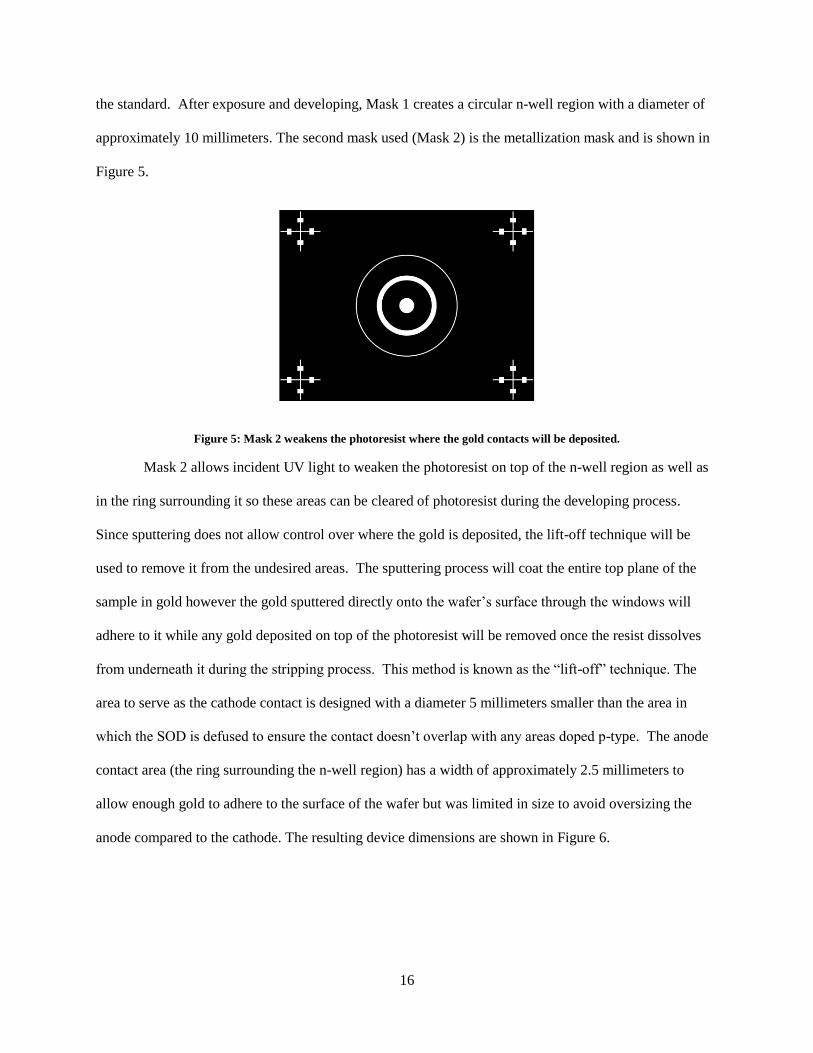
Figure 5: Mask 2 weakens the photoresist where the gold contacts will be deposited. .............................. 16
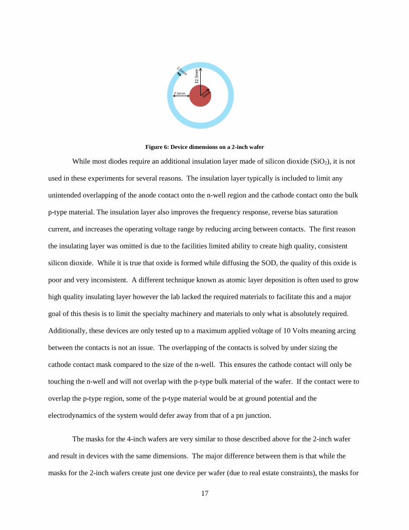
Figure 6: Device dimensions on a 2-inch wafer ......................................................................................... 17
Figure 7: Mask 1 for the 4-inch wafers creates the n-well as well as an n-type isolation region to decouple
the co-located devices. ................................................................................................................................ 18
Figure 8: Mask 2 for the 4-inch wafers clears the photoresist from the regions of the device where the
anode and cathode contacts will be sputtered. ............................................................................................ 18
Figure 9: a) Top view of configuration with both contacts on the top surface of the wafer and the resulting
electric fields aligned pointing radially inwards. b) Side view of top contact configuration showing charge
distribution throughout the thickness access. c) Top view of the non-collocated contact configuration with
the anode contact on the bottom of the wafer and the cathode on the top. d) Side view of the non-
collocated contact configuration showing the resulting electric fields aligning along the wafer thickness
axis. ............................................................................................................................................................. 19
Figure 10: Modified Mask 1 used for the process variation sample. .......................................................... 25
Figure 11: Current Voltage relationship of the Proof of Concept Sample .................................................. 30
Figure 12: Diode voltage (Vd) vs. Diode current (Id) for both the top and bottom contacts of the contact
comparison sample. ..................................................................................................................................... 32

viii
Figure 13: Diode voltage (Vd) vs. Log10 of the diode current for both the top and bottom contacts of the
contact comparison sample to better illustrate the relationship despite the large difference in magnitudes
between samples. ........................................................................................................................................ 32
Figure 14: This graph compares the I-V characteristics of the deep diffusion heating profile to those of the
short diffusion profile's. .............................................................................................................................. 35
Figure 15: Test circuit 1 used to measure the diode I-V relationship including the series resistances caused
by the sheet resistance, contact resistance, and resistance cause by the test lead connections. .................. 36
Figure 16: The individual I-V relationship for the sample created using the short diffusion profile and the
relationship calculated using the Matlab generated coefficients. ................................................................ 36
Figure 17: The individual I-V relationship for the sample created using the deep diffusion profile and the
relationship calculated using the Matlab generated coefficients. ................................................................ 37
Figure 18: The results of the process variation experiment are shown in the above I-V graph. It shows the
Manufacturer's recommended deposition method and the Diffuse through photoresist method. ............... 40
Figure 19: I-V relationship for the sample created using the Manufacturer recommended process and the
projected relationship calculated using the coefficients generated using Matlab. ...................................... 41
Figure 20: I-V relationship for the sample created using the Diffuse through photoresist process and the
projected relationship calculated using the coefficients generated using Matlab. ...................................... 41
Figure 21: Semi-log plot showing deviations from the ideal diode and the causes. A) Thermal
recombination in the depletion region. B) Ideal region. C) High-level injection. D) Series resistance
(Pierret, 1996) ............................................................................................................................................. 43
Figure 22: I-V curve of the device created on a 4-inch wafer using the short diffusion profile to diffuse the
n-type SOD through the photoresist using the coplanar top contact configuration. ................................... 55
Figure 23: Major and minor flat locations to determine doping type. ........................................................ 56
Figure 24: Mask 1 always incident UV light to penetrate the mask through the circle in the center. This
will weaken the photoresist underneath the circle. After the developing, a window will be opened through
which the SOD can be diffused................................................................................................................... 58

ix
Figure 25: Mask 2 always the incident UV light to penetrate the mask through the circle in the center as
well as the thicker ring around it. This will weaken the photoresist underneath those areas. After
developing, windows will be opened for the contacts. ............................................................................... 59
Figure 26: Overall device dimensions resulting from masks 1 and 2. ........................................................ 59
Figure 27: Dynalon 409224 HDPE hydrofluoric acid safe, flat bottom developing tray used to soak the
wafer in the buffered HF etchant during the oxide etch. ............................................................................. 62
Figure 28: Blank 2-inch P-type, silicon wafer. ........................................................................................... 62
Figure 29: Wafer coated with positive photoresist. .................................................................................... 63
Figure 30: Proper alignment of the mask to the wafer using the alignment ring. ....................................... 64
Figure 31: (a) Schematic cross section view of the processes performed above. (b) Top view of the wafer
post developing ........................................................................................................................................... 65
Figure 32: Diffusion heating profile showing Temperature vs. Time ........................................................ 67
Figure 33: Wafer coated with SOD............................................................................................................. 68
Figure 34: Sample structure after the diffusion/drive in bake. .................................................................... 69
Figure 35: Sample structure after the removal of the photoresist and excess SOD .................................... 69
Figure 36: Sample structure after the oxide and surface SOD strip. ........................................................... 70
Figure 37: Sample structure after the second photoresist application. ........................................................ 72
Figure 38: Proper alignment of the mask to the wafer using the alignment ring. ....................................... 73
Figure 39: (a) Schematic cross section view of the processes performed above. (b) Top view of the wafer
post developing ........................................................................................................................................... 74
Figure 40: SPI Sputtering Module and chamber. ........................................................................................ 74
Figure 41: The sputtering chamber during the sputtering process. ............................................................. 75
Figure 42: (a) Schematic cross section view of the sputtering process and the resulting sample. (b) Top
view of the wafer post sputtering ................................................................................................................ 76
Figure 43: Sample representation after the photoresist strip in acetone. .................................................... 77
Figure 44: Circuit configuration used to generate the I-V curves of the devices. ....................................... 78

x
Figure 45: Example I-V chart. .................................................................................................................... 78
Figure 46: Sample I-V curve captured using a Tektronix Type 576 curve tracer. ...................................... 79
1
Chapter 1: Introduction
Section 1.1: Semiconductor Prototyping:
Semiconductor devices and integrated circuits (ICs) are at the core of modern day
electronics, and the is significant interest in providing undergraduate students with hands-on
experience in device and IC fabrication (Naseem & Brown, 1999; Neudeck & Luginbuhl, 1970;
Neudeck, Luginbuhl, & Silva, 1970; Szmyd, 1995). Traditional approaches to semiconductor
device prototyping are expensive and time consuming, making them impractical and challenging
for most universities that do not have established integrated circuit fabrication facilities.
Semiconductors rely heavily on added impurities in intrinsic (pure) materials to change their
electrical, physical, and optical properties. This process is known as “doping”. Doping of
semiconductors requires specialty machines, personnel, and facilities. In traditional
semiconductor device fabrication, the doping is done using ion implantation, chemical vapor
deposition, or specialty doping furnaces. Ion implantation uses ionized molecules of the dopant
material accelerated by an electric field towards the target substrate to dislodge atoms of the
substrate material loose and inserting dopant atoms in their place. In specialty diffusion
furnaces, the dopant atoms are incorporated into the substrates atomic structure from toxic gases
at very high temperatures. In chemical vapor deposition (CVD), two specialty furnaces are
required and the handling of toxic, poisonous, and sometimes explosive make it extremely
unfavorable for students and other non-professionals in that field. For universities without such
facilities, the only option is to send them to commercial venders, which is extremely expensive
and time consuming. Additionally, all the doping processes above use toxic gases or extremely
high voltages creating safety hazards for users. Ion implantation devices operate at energies
2
ranging from 10 to 500 kilo-electron volts to accelerate the ions into the substrate, causing
damage to the crystalline structure which then requires a thermal annealing to repair crystalline
structure. This extra process results in longer process time as well as higher cost. The clean
room facilities required for these processes cost between $2500 per square foot to $6000 per
square foot to construct which further adds to the cost of these processes. For example, Intel’s
“D1X” facility in Hillsboro, Oregon cost around $6 billion to build and an estimated $60 million
per year to operate (not including personnel or the specialty machines inside the facility). Spin
on dopants (SODs) can significantly reduce universities’ reliance on such facilities by allowing
instructors and students to dope materials using their own facilities with minimal equipment
required.
A major goal of this research is to develop a process for the fabrication of semiconductor
devices and simple integrated circuits while avoiding ion implantation or specialty diffusion
furnaces by using SODs. SODs are a more recent advancement in doping technology (patented
in 1985). These SODs have not become wide spread because the early versions were expensive,
difficult to use, and lacked precision. Recent technological breakthroughs in material sciences
have led to much cheaper and more user friendly versions of these SODs, giving them the
potential to become very widely used. Since this newer technique has not been commonly used
in the past, data concerning the process requirements are somewhat unknown. This thesis will
outline the process requirements such as developers, etchants, soft bake and hard bake
parameters, photolithography procedures and techniques.
3
Section 1.2: Photolithography Masks:
Photolithography masks are another issue encountered when developing semiconductor
devices at the prototype level. Very simplistic device designs usually require between 3 and 5
different material layers which in turn, require an equal amount of masks. A non-complex,
relatively low resolution mask design (such as the designs used in this thesis) usually costs
between $300 and $500 each (aBeam Technologies, Inc., 2016) putting the total cost around
$1600. In addition to the cost of the mask fabrication itself, the design software normally used to
develop and submit the mask designs for fabrication can cost upwards of $3000 (Artwork
Conversion Software, Inc., n.d.) The process developed for this research utilizes transparency
film (available from any office supply store), laser jet printers (standard office equipment), and
PowerPoint (standard software) to design and create photolithography masks for a few cents
each. The low cost and ease of fabrication associated with this mask making technique promotes
rapid design modification. Historically, the laboratories at the University of Nevada, Las Vegas
(UNLV) have taught photolithography using the transparency film technique but have been
unable to produce working devices from it. The alignment techniques and mask design
fundamentals outlined in this thesis will enable users to produce functioning devices which can
then be used to teach characterization and semiconductor device testing techniques.
Section 1.3: Education:
These issues make prototyping semiconductor devices very difficult and educational
laboratory courses nearly impossible. The lead time per process run exceeds the duration of
most college semester making it impossible to teach a course in which students design, fabricate,
and characterize their own semiconductor devices. Additionally, the cost associated is beyond
4
what most universities are able to provide to professors for course expenses. While learning
about semiconductor devices, it is important to understand the process by which they are made to
better grasp the physics behind the operation of such devices. This deeper understanding leads to
recognition of the limitations and design flaws of the devices and allows for adjustments and
“fine tuning” of these designs to yield better solutions which can then be prototyped locally in
the universities’ labs. If the prototyping process is too costly (in time and/or money), it is a very
slow process which impedes progress and innovation.
The pn junction diode has been chosen as the device for the demonstration of this process
due to its importance, simplicity, and versatility. The pn junction is the base structure for solar
cells, bipolar junction transistors (BJTs), and light emitting diodes (LEDs). It is because of these
device’s reliance on the pn junction that it is usually the first presented in undergraduate courses
on semiconductors due to its fundamental nature so providing students and professors with a
process by which they can design and fabricate diodes locally will provide greater continuity to
university courses.
Several process variations are presented in this paper in an effort to determine how
certain changes in the techniques affect the overall devices. The first variation concerns the
anode contact location. As part of the lab generated from these experiments, students will
deposit three contacts onto the samples. A cathode and an anode contact are deposited on the
polished top surface of the wafer, with a second anode contact on the bottom side of the wafer.
As explored in the “Contact Comparison” experiment, this configuration allows a direct
comparison of how the contacts affect device characteristics. The second variation adjusts the
diffusion temperature profile to determine if a short rapid diffusion produces favorable current-
voltage relationships than a longer diffusion time which is presented in the “Diffusion Profile”
5
experiment. The third process variation concerns the order of the process steps. The
manufacturer recommends depositing the SOD first however the associated difficulties of this
process can be avoided by diffusing the SOD through windows opened in the photoresist. The
“Process Variation” experiment will determine if there are adverse effects caused by diffusing
the SOD through the photoresist rather than using the manufacturer recommended method.
In addition to developing processes to fabricate devices using Spin-On dopants, device
characterization techniques are also presented to allow process variations and techniques to be
compared on a device by device level in order to determine which process steps should be used
in order to create the highest performing devices.
Using only the information in this thesis, professors and students will be able to recreate
the devices presented here within with little to no modification of the design and fabrication
processes. Although modification to these processes will not be necessary to reproduce these
semiconductor devices, it is encouraged in the hopes that improvements to both the processes
and devices are discovered and implemented.
6
Chapter 2: Background
In order to create a pn junction, an intrinsic material such as silicon or gallium arsenide is
doped by a carefully controlled addition of dopant atoms. Silicon, for example, is a group 4
element meaning it has 4 electrons in its outer shell. When a group 3 element (i.e. boron) is
inserted into a crystalline silicon lattice structure, the resulting covalent bond has 7 electrons in
the valence band leaving 1 position open for another electron (known as a hole). Because
electrons are negatively charged, most theories treat this “hole” as a positively charged particle.
This molecule formed between the boron and silicon atoms is now positively charged and this
process repeated periodically throughout the substrate material yields an overall positively doped
material or p-type. If a similar process was repeated with the substitution of a group 5 element
(i.e. phosphorus) for boron, the overall silicon-phosphorus molecule would have 9 electrons.
Because it takes 8 electrons to achieve covalent bonding, the extra electron would cause the
molecule to be negatively charged. Repeating this process periodically throughout the substrate
would yield an overall negatively doped material or n-type. A pn junction is then formed by
diffusing n-type dopants into a p-type substrate in a large enough volume to leave the targeted
area doped n-type overall. The reverse of this technique is also used (p-type dopants into an n-
type substrate). Simple pn junction diodes are considered to be the building blocks of most
modern and more complex semiconductors such as bipolar junction transistors and metal-oxide
field effect transistors (BJTs and MOSFETS respectively).
Most research into semiconductor fabrication using SOD has been in the field of solar
energy, specifically photovoltaic cells. The main reasons for this are the desire for low cost,
mass production capability, along with the large size of the cells.
7
The work performed by Hamammu and Ibrahim (2003) have shown promising results
using the same SOD as the experiments for this thesis. Typically, diffusion takes place in two
steps; the short duration, high concentration, constant source pre-diffusion to create an impulse
dose at the surface of the wafer, and the longer drive in bake to diffuse the dopants into the
lattice structure. Unfortunately, the two step process requires two different specialty furnaces to
perform leading to increased expense. Additionally, since the sample has to be transferred
between furnaces between steps, additional impurities along with surface and lattice defects
result. By using a single drive in baking process, these imperfections and defects are avoided
and the complications and expense of the process are reduced. In the study by Hamammu and
Ibrahim (2003), they began with 5-inch, p-type silicon wafers with a resistivity of 1 Ω-cm. The
SOD was then spun onto the wafer and hard baked at 200 °C for 30 minutes. These are the
manufacturer recommended hard bake parameters when using an evaporation oven as opposed to
a hotplate. The samples were then inserted into the diffusion furnace at 750 °C at which point
the temperature was slowly increased to 1050 °C then back down to 750 °C. The referenced
work does not provide detail concerning the heating rate, the time allowed for diffusion, or the
cooling rate. A mixture of these parameters and those provided by the manufacturer will be
applied to the experiments in this thesis. A common technique in solar cell processing is
“texturing” of the wafer’s surface that allows the active area of the device to be increased
without changing the overall dimensions. The technique uses alkaline solutions, plasma, reactive
ion etching (RIE), or mechanical methods to cut v-groves into the wafers surface. The result of
the texturing process is an improvement in solar cell current and higher efficiency. In flat silicon
substrates, a portion of the incident radiation is reflected back from the surface. Texturing
created pyramidal structures on the wafers surface that redirect the reflected energy towards the
8
side of the structure allowing a portion of the reflected incident radiation to be absorbed before it
is reflected again (shown in Figure 1).
Figure 1: The texturing technique improves cell efficiency by capturing some of the reflected radiation by directing it
toward the side of the pyramid structures etched into the wafer surface. (Honsberg & Boden, n.d.)
The texturing technique is only applicable to high quality, monocrystalline substrates with
certain lattice orientations. Using SODs and texturing the surfaces of the wafer, Hamammu and
Ibrahim (2003) were able to create solar cells with an efficiency of 17.1% while simplifying the
diffusion process and reducing the amount of specialty equipment required. The I-V curve
showing their best results is shown in Figure 2.
Figure 2: I-V curve of the sample with the best results from (Hamammu & Ibrahim, 2003).
When analyzing the I-V curves of photovoltaic cells, it is important to realize that while
solar cells are essentially specialized diodes, the curves shown are not obtained using the same
measurements as other diodes. In photovoltaic cells, the current at zero volts is actually the short
circuit current of the device (output terminals shorted) with a known amount of incident radiation
9
onto the cell. The zero current point on the curve is the open circuit voltage and is measured by
applying the same amount of incident radiation and measuring the voltage at the outputs. The
rest of the curve is obtained by varying the load connected to the output terminals of the device
while applying the same amount of incident radiation to the cell. This is in contrast to typical
diode characterization in which the supply voltage is applied between the anode and cathode then
incremented while taking circuit current measurements to map the current response to each
applied voltage.
Homojunction solar cells formed using silicon substrates are still the primary source of
photovoltaic cells despite being the oldest and years of research into alternative technologies.
Although the cost of manufacture is high, the silicon homojunction remains the most popular
base due to the high efficiency and reliable operation. The associated cost has significantly
impacted the popularity of solar cells as an alternative energy source. Teh and Chuah (1989)
have shown SODs can be used to significantly decrease manufacturing costs of solar cells by
avoiding traditional deposition and doping processes, such as chemical vapor deposition. Their
work titled, “Diffusion profile of spin-on dopant in silicon substrate” focuses mostly on the
characteristics of silicon wafers after the diffusion of phosphorus based SODs.
Teh and Chuah (1989) started their process with boron-doped silicon wafers with a 5 cm
diameter, 300 µm thickness, and a starting resistivity of 0.17-0.20 Ω-cm. Based on the starting
resistivity of their wafers, it is estimated the p-type doping density is between 9*1016 and 1*1017
cm-3. Given that the generally accepted degenerate doping level for p-type dopants in silicon
substrates is 9.1*1017 cm-3, the starting wafers are considered to be non-degenerately doped
making analysis and device characterization calculations less difficult and more accurate. They
then proceeded to coat the wafer with Accuspin PX-10 Spin-On dopant and spun at 2500 rpm for
10
25 seconds in 30% humidity. The SOD used in their study is phosphorus based and is very
similar to the one used in the experiments for this thesis. The humidity was found to be a critical
parameter when applying the SOD. If deposited in too high a humidity, the SOD becomes
cloudy due to extra water absorption from the atmosphere and results in a poor quality diffusion.
The wafer was then cured at 150 °C for 10 minutes in an exhaust oven. The curing process is
similar to hard baking of photoresist and improves the adhesion of the SOD to the wafer surface.
The drive in or diffusion bake was performed for one hour in a temperature range from 900 ° to
1150 °C in a non-oxidizing ambient. The non-oxidizing diffusion atmosphere was achieved by
flowing a steady stream of nitrogen across the face of the wafer. This leads to lower sheet
resistance and a higher quality diffusion. They found that the phosphorus based SODs follow the
Fair-Tsai model for phosphorus diffusion into silicon substrates (Fair & Tsai, 1977) which is
interesting given the diffusion techniques used at the time that model was discovered were
different from those used now. Teh and Chuah (1989) also found that for substrate background
doping densities greater than 1.67*1017 cm-3, the phosphorus diffusion profile was altered and
some of the diffusants were rendered electrically inactive due to the mass-action between the
phosphorus and the original boron atoms used to dope the substrate. Upon completion of the
sample fabrication, they were measured using a collinear four probe array in 5 locations on the
wafers surface. The measured sheet resistances varied by less than 2% for all locations meaning
the diffusion profile of phosphorus based SODs is very uniform and consistent. The resulting
post diffusion n-type surface concentration was found to be approximately 1*1021 cm-3 which is
considered degenerately doped for n-type diffusants in silicon. The humidity control during the
SOD application was found to be crucial. If the humidity is too low, the alcohol present in the
SOD solution evaporates and creates a transparent coating. If the humidity is too high, the

11
solution absorbs water from the atmosphere and becomes cloudy in appearance. Both situations
lead to a poor quality diffused layer with higher surface and lattice defects. They developed an
equation to calculate the junction depth of the dopants based on temperature given by Equation 1.
Equation 1: Junction depth of phosphorus diffusants in silicon (Teh & Chuah, 1989)
ln(𝑥𝑗) = (1.51
𝑘𝑇) + 13.96
This equation will be used to estimate the junction depth of SOD diffusants resulting from the
diffusion properties used in this thesis. While the equation doesn’t explicitly state a time
dependence, it is assumed to be per hour of drive in bake.
The techniques presented in these works concerning the diffusion temperatures, the
conditions for wafer coating using SOD, and the diffusion profile of phosphorus based SODs
will be applied to the experiments in this thesis.
12
Chapter 3: Experimental Design
As presented in the introduction chapter, the focus primary of this thesis is developing a process
by which semiconductor devices and circuits can be fabricated using spin-on dopants and
photolithography. The foundation of modern semiconductor devices is the pn junction structure. This
structure is integral in devices such as diodes, bi-polar junction transistors, metal oxide field effect
transistors, and photo sensors. The physics of the pn junction is discussed in the background chapter of
this thesis. It is important to understand the experiments presented herewith are designed for use in the
clean room facility at the University of Nevada, Las Vegas by students. These processes can easily be
adapted for more complicated devices and circuits requiring higher precision parameters. The following
experiments will use solution P509 by Filmtronics. P509 is a spin-on dopant comprised of 15 percent
phosphorus, 5 percent silicon dioxide (𝑆𝑖𝑂2), and a proprietary solution not released to users. While the
primary use of this SOD is for solar cell fabrication, it is still a valid choice because the base device of
solar cells is the diode. Although SOD’s designed specifically for pn junction diodes are available, using
them would increase cost and limit other uses for the solution. Since the main users of this process will
be universities and students, it is not advisable to use limited application materials when a broader
spectrum solution is available. The level of detail and specificity presented in the following sections is
done so intentionally to promote exact replication of the experiments by other institutions and researchers.
All device samples were prepared on p-type silicon wafers with either 2-inch or 4-inch diameters. The
process step common to all samples is the wafer cleaning process. It is described in the paragraph below
in detail to promote safety and repeatability however all subsequent samples will describe it only as
“wafer cleaning”.
Section 3.1: Proof of Concept Experiment
In order to validate further experiments, the plausibility of creating pn junction diodes using the
equipment available in the local labs at UNLV was first tested by creating a proof of concept sample. The

13
proof of concept applies only the most basic and necessary portions of the overall process in order to
demonstrate that diffusion of an n-type SOD into a p-type wafer creates a very basic pn junction diode.
No photolithography is used during the proof of concept in order to limit the number of potential
complications. Before beginning the diffusion process, a 2-inch, p-type, silicon wafer must be cleaned
using the piranha cleaning procedure outlined in Table 3 of Appendix A1. This is necessary because it
removes any oxidation from the surface of the wafer promoting strong adhesion between the wafer’s
surface and the SOD. Once the cleaning process has been completed, the wafer is placed onto the spin
coater machine to be coated with SOD. As always, it is important to remove the SOD from refrigeration
24 hours before deposition to allow it to acclimate to room temperature. Using the parameters listed in
Table 6 in Appendix A2, 1 ml of P509 Spin On Dopant is applied to the wafer using a pipette and the start
button pressed. Once the spin coater has finished the programmed routine, a soft bake must be performed
to harden the SOD before diffusion. The wafer is removed from the machine, wrapped in aluminum foil
for easy handling, placed into an air convection oven preheated to 100 °C and allowed to bake for 15
minutes. The soft bake solidifies the SOD by evaporating the ethyl alcohol solvents incorporated in the
solution for easy deposition. The solvents absorb the heat radiation which decreases the photo-
solubilization effect and their resistance to adhesion. The furnace temperature controller is then
programmed using the settings provided in Table 7 of Appendix A3 and the program is started. More
detailed instructions for programming the temperature controller are included in Appendix A3. The
furnace heating profile parameters (listed in Table 7) result in an increase in the chamber temperature
from 26 °C to 1100 °C over a period of 2 hours and 15 minutes, remain at 1100 °C for 2.5 hours, then
reduce the temperature back down to 26 °C (room temperature). The diffusion heating profile used in the
proof of concept experiment allows for a longer diffusion time at 1100 °C than the other heating profile
presented in this thesis and will be referred to as the “deep diffusion” profile. A graphical representation
of this profile is shown below in Figure 3. The manufacturer recommends that the SOD be diffused in a
diffusion temperature of 1100 °C in a 25% oxygen and 75% nitrogen atmosphere for 2.5 hours in order to
yield a sheet resistance of 2.1 Ω/square. To reduce complexity, a pure oxygen environment is used during
14
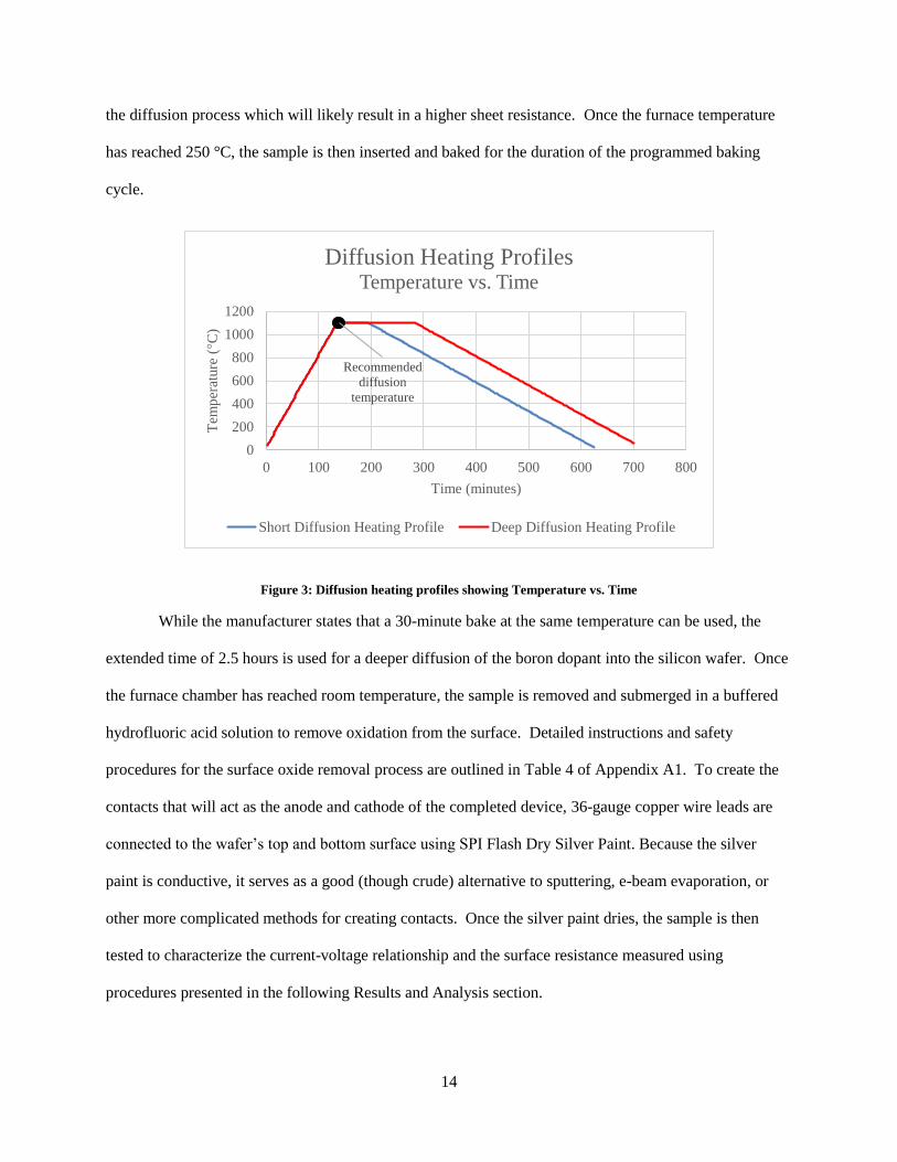
the diffusion process which will likely result in a higher sheet resistance. Once the furnace temperature
has reached 250 °C, the sample is then inserted and baked for the duration of the programmed baking
cycle.
Figure 3: Diffusion heating profiles showing Temperature vs. Time
While the manufacturer states that a 30-minute bake at the same temperature can be used, the
extended time of 2.5 hours is used for a deeper diffusion of the boron dopant into the silicon wafer. Once
the furnace chamber has reached room temperature, the sample is removed and submerged in a buffered
hydrofluoric acid solution to remove oxidation from the surface. Detailed instructions and safety
procedures for the surface oxide removal process are outlined in Table 4 of Appendix A1. To create the
contacts that will act as the anode and cathode of the completed device, 36-gauge copper wire leads are
connected to the wafer’s top and bottom surface using SPI Flash Dry Silver Paint. Because the silver
paint is conductive, it serves as a good (though crude) alternative to sputtering, e-beam evaporation, or
other more complicated methods for creating contacts. Once the silver paint dries, the sample is then
tested to characterize the current-voltage relationship and the surface resistance measured using
procedures presented in the following Results and Analysis section.
Recommended
diffusion
temperature
0
200
400
600
800
1000
1200
0 100 200 300 400 500 600 700 800
Tem
per
ature
(°C
)
Time (minutes)
Diffusion Heating ProfilesTemperature vs. Time
Short Diffusion Heating Profile Deep Diffusion Heating Profile
15
Section 3.2: Mask Design and Fabrication
In order to improve the device characteristics over those exhibited by the proof of concept
sample, the dimensions of the devices must be adjusted to create smaller active surfaces. To do this,
photolithography techniques are employed to control the size of the wafer doped n-type (the n-well), the
size of the contacts, and the spacing between them. The first step in the photolithography process is to
design masks that will result in the desired device dimensions. There are 2 masks used in each of the
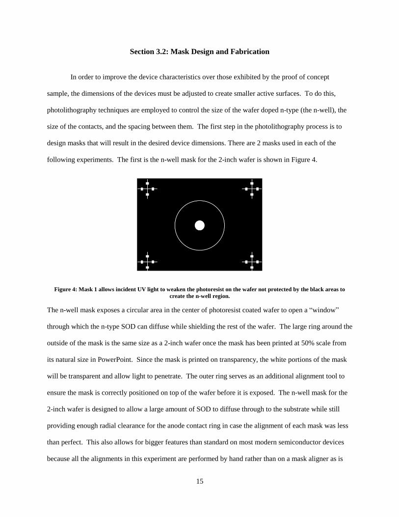
following experiments. The first is the n-well mask for the 2-inch wafer is shown in Figure 4.
Figure 4: Mask 1 allows incident UV light to weaken the photoresist on the wafer not protected by the black areas to
create the n-well region.
The n-well mask exposes a circular area in the center of photoresist coated wafer to open a “window”
through which the n-type SOD can diffuse while shielding the rest of the wafer. The large ring around the
outside of the mask is the same size as a 2-inch wafer once the mask has been printed at 50% scale from
its natural size in PowerPoint. Since the mask is printed on transparency, the white portions of the mask
will be transparent and allow light to penetrate. The outer ring serves as an additional alignment tool to
ensure the mask is correctly positioned on top of the wafer before it is exposed. The n-well mask for the
2-inch wafer is designed to allow a large amount of SOD to diffuse through to the substrate while still
providing enough radial clearance for the anode contact ring in case the alignment of each mask was less
than perfect. This also allows for bigger features than standard on most modern semiconductor devices
because all the alignments in this experiment are performed by hand rather than on a mask aligner as is
16
the standard. After exposure and developing, Mask 1 creates a circular n-well region with a diameter of
approximately 10 millimeters. The second mask used (Mask 2) is the metallization mask and is shown in
Figure 5.
Figure 5: Mask 2 weakens the photoresist where the gold contacts will be deposited.
Mask 2 allows incident UV light to weaken the photoresist on top of the n-well region as well as
in the ring surrounding it so these areas can be cleared of photoresist during the developing process.
Since sputtering does not allow control over where the gold is deposited, the lift-off technique will be
used to remove it from the undesired areas. The sputtering process will coat the entire top plane of the
sample in gold however the gold sputtered directly onto the wafer’s surface through the windows will
adhere to it while any gold deposited on top of the photoresist will be removed once the resist dissolves
from underneath it during the stripping process. This method is known as the “lift-off” technique. The
area to serve as the cathode contact is designed with a diameter 5 millimeters smaller than the area in
which the SOD is defused to ensure the contact doesn’t overlap with any areas doped p-type. The anode
contact area (the ring surrounding the n-well region) has a width of approximately 2.5 millimeters to
allow enough gold to adhere to the surface of the wafer but was limited in size to avoid oversizing the
anode compared to the cathode. The resulting device dimensions are shown in Figure 6.
17
Figure 6: Device dimensions on a 2-inch wafer
While most diodes require an additional insulation layer made of silicon dioxide (SiO2), it is not
used in these experiments for several reasons. The insulation layer typically is included to limit any
unintended overlapping of the anode contact onto the n-well region and the cathode contact onto the bulk
p-type material. The insulation layer also improves the frequency response, reverse bias saturation
current, and increases the operating voltage range by reducing arcing between contacts. The first reason
the insulating layer was omitted is due to the facilities limited ability to create high quality, consistent
silicon dioxide. While it is true that oxide is formed while diffusing the SOD, the quality of this oxide is
poor and very inconsistent. A different technique known as atomic layer deposition is often used to grow
high quality insulating layer however the lab lacked the required materials to facilitate this and a major
goal of this thesis is to limit the specialty machinery and materials to only what is absolutely required.
Additionally, these devices are only tested up to a maximum applied voltage of 10 Volts meaning arcing
between the contacts is not an issue. The overlapping of the contacts is solved by under sizing the
cathode contact mask compared to the size of the n-well. This ensures the cathode contact will only be
touching the n-well and will not overlap with the p-type bulk material of the wafer. If the contact were to
overlap the p-type region, some of the p-type material would be at ground potential and the
electrodynamics of the system would defer away from that of a pn junction.
The masks for the 4-inch wafers are very similar to those described above for the 2-inch wafer
and result in devices with the same dimensions. The major difference between them is that while the
masks for the 2-inch wafers create just one device per wafer (due to real estate constraints), the masks for
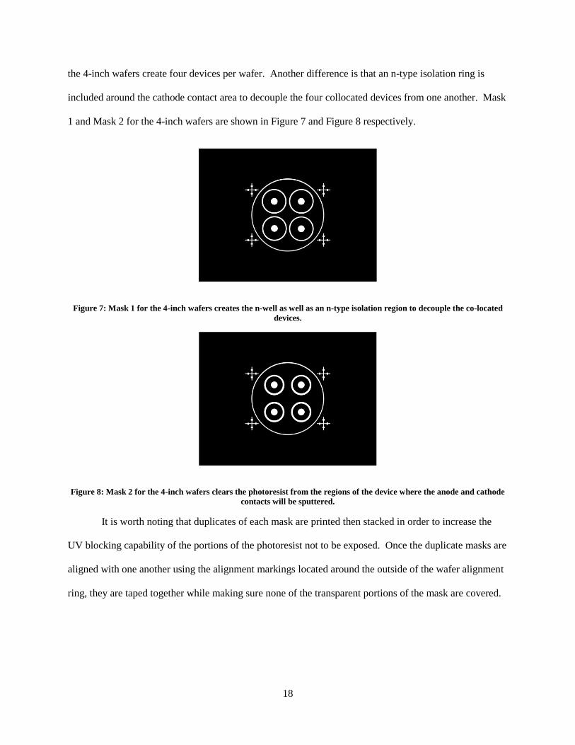
18
the 4-inch wafers create four devices per wafer. Another difference is that an n-type isolation ring is
included around the cathode contact area to decouple the four collocated devices from one another. Mask
1 and Mask 2 for the 4-inch wafers are shown in Figure 7 and Figure 8 respectively.
Figure 7: Mask 1 for the 4-inch wafers creates the n-well as well as an n-type isolation region to decouple the co-located
devices.
Figure 8: Mask 2 for the 4-inch wafers clears the photoresist from the regions of the device where the anode and cathode
contacts will be sputtered.
It is worth noting that duplicates of each mask are printed then stacked in order to increase the
UV blocking capability of the portions of the photoresist not to be exposed. Once the duplicate masks are
aligned with one another using the alignment markings located around the outside of the wafer alignment
ring, they are taped together while making sure none of the transparent portions of the mask are covered.
19
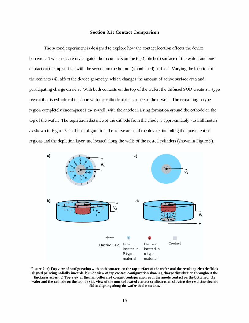
Section 3.3: Contact Comparison
The second experiment is designed to explore how the contact location affects the device
behavior. Two cases are investigated: both contacts on the top (polished) surface of the wafer, and one
contact on the top surface with the second on the bottom (unpolished) surface. Varying the location of
the contacts will affect the device geometry, which changes the amount of active surface area and
participating charge carriers. With both contacts on the top of the wafer, the diffused SOD create a n-type
region that is cylindrical in shape with the cathode at the surface of the n-well. The remaining p-type
region completely encompasses the n-well, with the anode in a ring formation around the cathode on the
top of the wafer. The separation distance of the cathode from the anode is approximately 7.5 millimeters
as shown in Figure 6. In this configuration, the active areas of the device, including the quasi-neutral
regions and the depletion layer, are located along the walls of the nested cylinders (shown in Figure 9).
Figure 9: a) Top view of configuration with both contacts on the top surface of the wafer and the resulting electric fields
aligned pointing radially inwards. b) Side view of top contact configuration showing charge distribution throughout the
thickness access. c) Top view of the non-collocated contact configuration with the anode contact on the bottom of the
wafer and the cathode on the top. d) Side view of the non-collocated contact configuration showing the resulting electric
fields aligning along the wafer thickness axis.
20
In the second configuration, with the cathode on the top of the wafer and the anode on the bottom,
the geometry doesn’t change very much from the first configuration however the active surfaces do. The
second configuration is more dependent on the diffusion depth and the resulting metallurgical junction.
Since the 2-inch wafer used in this experiment is approximately 300 micrometers thick, it is not plausible
for the SOD to diffuse through the entire thickness of the wafer. Another consequence of separating the
contacts onto separate surfaces is the aligning of the electric fields inside the device. With the contacts
located in line along the wafer’s thickness axis, the electric field vectors point directly from the anode to
the cathode as opposed to radially inward as is the case with the contacts on the same surface plane. To
ensure the contact location is the only variable effecting the device characteristics, both contact
configurations are deposited on the same device sample.
The first process performed on the contact comparison sample is the wafer cleaning. Upon
completing the cleaning process, the wafer is transferred to the spin coater machine to be coated with
photoresist. Every potion of this experiment and those to follow not involving HF or sample cleaning
will take place in the lithography room designed to limit undesired exposure of the sensitive chemicals to
light. Using the parameters listed in Table 5 of Appendix A2, 2 ml of PR1-1000A photoresist is applied
to the wafer using a pipette and the start button pressed. Once the spin coater has finished the
programmed routine, a soft bake must be performed to harden the photoresist before photolithography can
be performed. The soft bake solidifies the photoresist enough to adhere to the wafer while still leaving it
vulnerable to the ultraviolet rays used to weaken the areas to be removed during development. The
evaporation oven is preheated to 90 °C and the wafer is transferred from the vacuum chuck of the spin
coater to the oven once it has reached temperature. The wafer then remains baking for 20 minutes at
which point it is removed from the oven and allowed to cool. Once the sample has acclimated to room
temperature, it is moved to the photolithography station. The sample is then placed in an alignment
device to keep the major flat oriented perpendicular to the alignment platform as this makes it easier to
align the masks to follow. The transparency masks are created in Microsoft PowerPoint and the files are

21
available upon request via the email address included in this thesis however a brief description of the
dimensions is included. Mask 1 (n-well mask) is then placed onto the sample while making use of the
transparent alignment ring to center it. The photoresist used for this experiment was purchased recently
so it will not require as much exposure time as an older batch would. The UV source is then powered on
40 seconds then powered off. This is all the exposure time required in this case since the photoresist is
new. Older batches closer to the expiration date will require more exposure time than listed here however
if the pattern fails to appear with defined lines and edges during developing, the sample can be exposed
again then redeveloped being sure to align the mask and sample as closely as possible to their placement
during the first exposure to avoid a “ghosting” effect. The wafer is then transferred from the
photolithography station to the development station located inside the chemical fume hood. To perform
the photolithographic developing, approximately 30 milliliters of Futurrex RD6 resist developer is poured
into a chemical safe dish. The sample is the submerged in the developer solution for approximately 20
seconds or until the features are well defined. Once again, the age of the photoresist and developer
greatly affects the development time. Once the developing is completed, the sample is submerged in a
deionized water for rinsing and dried using a nitrogen gun. The wafer is then transferred to the
evaporation oven preheated to 100 °C to perform the hard bake. The sample is to remain in the
evaporation oven for 30 minutes. The hard bake further solidifies any photoresist remaining on the
sample’s surface so it can retain its pattern during the drive in bake. Once the hard bake has been
completed, the sample is set aside and allowed to cool. The sample is then transferred to the spin coater
for the application of the SOD. The spin coater is then programmed using the parameters in Table 6 of
Appendix A2, and 1 milliliter of SOD is applied to the sample using a pipette. The spin is started by
pressing the “start” button. Once the spin procedure has completed, the wafer is removed from the
vacuum chuck of the spin coater and transferred to an aluminum foil wrap until the diffusion furnace has
preheated to 750 °C. In this experiment, the diffusion furnace is programmed using the parameters listed
in Table 8 of Appendix A3 which allows for a shorter diffusion time than that used during the proof of
concept experiment. A shorter diffusion is used during the contact comparison experiment to mitigate

22
any artifacts that may arise from too large a diffusion depth. A shallow diffusion is all that is needed for
an accurate analysis of the effect the contact location has on the overall device parameters. The settings
in Table 8 result in the diffusion heating profile shown in Figure 3.
Once the diffusion furnace has reached 750 °C, the sample is removed from the aluminum foil
warp and transferred to the furnace chamber where it remains until the entire programmed heating profile
has completed. Since this experiment uses the short diffusion heating profile, the full cycle (including
preheating) should take approximately 10 hours. After the furnace has completed the cycle, the sample is
removed and transferred to the chemical hood where the stripping process is performed. Before
performing the second (and last) round of photolithography for this sample, the remaining photoresist
from the first layer, the undiffused SOD, and the silicon dioxide (SiO2) formed during the baking process
must all be removed. The first step is similar to the lift off technique described in preceding sections in
that the removal of the lower layer of material will also remove the materials layered on top of it. The
sample is then submerged in a glass beaker containing approximately 30 milliliter of semiconductor grade
(99.5% pure) acetone to remove the photoresist and remaining SOD. A glass beaker is best suited for this
so it can be covered in aluminum foil and placed into the ultrasonic cleaner to expedite the process. Once
the majority of the remaining photoresist and SOD is removed, a soak in buffered HF is performed.
Using the same methods as in the proof of concept experiment, buffered HF is mixed in a HF safe plastic
container and the sample is submerged for 15 minutes to strip the oxides present on the wafer surface.
The same rinse procedure outlined in Table 4 is performed. The sample should now be clean and the top
surface should appear mirror-like. The sample is then coated with photoresist and a second soft baking is
performed using the same process used during the first photoresist application (again, using the same
parameters shown in Table 5.) The second round of photolithography creates the windows to allow the
sputtered gold onto the surface of the sample. After the soft bake is completed, the sample and mask are
aligned. The sample is then exposed through mask 2 (Figure 5) for 40 seconds to open the windows for
the contacts. The sample is then developed, rinsed, and transferred to the sputtering machine (the exact

23
model is listed in Table 11). A gold target is then loaded into the sputter coater head for deposition.
Once the sample is loaded into the sputtering chamber, the gas leak valve is closed, and the sputtering
machine control module is powered on to start removing air from the chamber. Once the vacuum gauge
reads approximately 101 millibar, the “Test” button is depressed to monitor the current drawn by the
plasma. If there is too much air in the sputtering chamber, the current draw will rise too high and create
gold layers of varying consistency and thickness. The gas leak valve is then opened slightly to adjust the
current flow up to approximately 30 milliamps. The “Start” button is then pressed and the sputtering
timer set to 240 seconds. Once the sputtering process is complete, the sputtering system is powered off
and the leak valve is opened to release the vacuum in the chamber. The sample is then submerged in a
beaker containing acetone and placed into the ultrasonic cleaner for 15 minutes to remove the photoresist
and excess gold. After all the excess gold and photoresist are removed, wires are connected to the sample
at the contact locations using silver conductive paint.
Section 3.4: Diffusion Profile Variation
Due to the amount of detail provided when describing the previous two experiments, from this
point on any procedure already described in the preceding paragraphs will be referenced by name and will
not include a description unless deviations from it are made. Instead of listing all the same process details
over again, the next experiment focuses on the effects the diffusion profile used on device characteristics.
Previously, both heating profiles were described and illustrated (in Figure 3). Since the contact
comparison sample is created using the short diffusion heating profile, only one additional sample making
use of the deep diffusion profile is required. This new sample, the diffusion profile comparison sample, is
fabricated using the same methods and process steps as the contact comparison sample except the deep
diffusion heating profile settings are used (Table 7 of Appendix A3) rather than the short diffusion
settings (Table 8). The difference in diffusion time between the two profiles is approximately 90 minutes.
This is a significant enough amount of time to noticeably change the device characteristics due to changes
in the location of the metallurgical junction, the sizes of the quasi-neutral zones, and the overall doping

24
density of the n-type regions of the device. The process to fabricate the diffusion profile comparison is
outlined in Table 1 rather than presented in this paragraph as previous processes have been for the sake of
brevity and because of its similarity to the process used to fabricate the contact comparison sample.
Step Process Step Instructions/Parameters
1 Wafer Cleaning Procedure outlined in Table 3.
2 Photoresist Coating #1 Using spin coater settings outlined in Table 5.
3 Soft Bake 20 minutes at 90 °C
4 Exposure #1 Using Mask 1 (Figure 4) and an exposure time of 40 seconds
5 Developing Submerge in developer solution for approximately 20 seconds
followed by DI water rinse.
6 Hard Bake 30 minutes at 100 °C
7 SOD Coating Using spin coater settings in Table 6.
8 Diffusion/Drive in bake Using the settings given in Table 7.
9 Photoresist and excess
SOD strip
Submerge in acetone and then placed the ultrasonic cleaner for
15 minutes.
10 Oxide Strip Procedure outlined in Table 4
11 Photoresist Coating #2 Repeat Step 2.
12 Soft Bake Repeat Step 3.
13 Exposure #2 Using Mask 2 (Figure 5), and an exposure time of 40 seconds.
14 Developing Repeat Step 5.
15 Sputtering Repeat the sputtering process performed on the contact
comparison sample to sputter gold for 240 seconds at ~ 30 mA.
16 Lift-Off Submerge in acetone and then placed in the ultrasonic cleaner for
15 minutes.
17 Wire placement Secure wires to the gold contacts using silver conducting paint.
Table 1: The process to fabricate the Diffusion profile Comparison sample.
Section 3.5: Process Variation
The next experiment presented is designed to study the effects process variations has on the
devices overall and will create the process variation sample. According to the SOD manufacturer
datasheet, the SOD is to be applied to the wafer (following the wafer cleaning) before any
photolithography is performed. This method will be referred to as the manufacturer recommended process
in the Results and Analysis section. In this process, the SOD is applied to the wafer first, followed by a
soft bake for 30 minutes at 200 °C. The sample is then coated with photoresist and soft baked for 20
minutes at 90 °C to solidify the resist. To change the sequence in which the process steps are performed,
a modified version of Mask 1 is used to expose and remove all of the photoresist coating the areas of the
25
wafer to remain p-type. The only resist remaining on the sample covers the portion of the wafer to that
will become the n-well. The modified “negative” version of mask 1 (shown below in Figure 10).
Figure 10: Modified Mask 1 used for the process variation sample.
The sample is then developed and the photoresist remaining is then hard baked. This causes the
remaining resist to polymerize allowing it to act as a shield for the SOD underneath. The rest of the SOD
is then removed using a buffered HF soak making sure not to dissolve the photoresist on top of the
remaining SOD. The HF soak should approximately 10 minutes. The buffered HF reacts and dissolves
the SOD but not the photoresist due to the polymerization caused by the hard bake. This process differs
from the methods used previously because rather than opening windows through which the SOD diffuses,
it instead removes all the SOD except what is to be diffused. The SOD is then diffused using the Short
diffusion heating profile, the settings for which are given in Table 8. Once the diffusion is completed, the
sample is submerged in acetone and placed in the ultrasonic cleaner for 20 minutes to dissolve the
protective layer of photoresist on top of the n-well. The sample is then cleaned using buffered HF (Table
4) to remove the remaining SOD and silicon dioxide. The contacts are then created by following steps 11
through 17 in Table 1. It is worth noting that although a modified version of mask 1 is used to create the
n-well, mask 2 (shown Figure 5) is still used to create the contacts. The sample to be used as the control
value during testing, is the contact comparison sample. This is done because the contact comparison
sample was also diffused using the same diffusion profile as the process variation sample and limits the
number of unforeseen variables during the device characterization.
26
Throughout this section, the steps and procedures performed result in the fabrication of 4 diode
samples. The methods described are designed to vary only one process variable per experiment in order
to minimize the number of free variables and their interactions. This improves the accuracy of the
analysis. In the contact comparison experiment, the two anode contacts are deposited on the same device
while both configurations will share the same cathode contact. By doing so the process steps, diffusion
profile, and doping density remain the same for both configurations with the only change being the
location of the anode. The diffusion profile variation experiment uses the contact comparison sample as
the control sample to save resources and testing time. Once again the samples are created using the same
process including the soft bake, hard bake, and contact placement. During the analysis to follow, the top
contacts of the contact comparison sample are used in order to match the placement of the contacts on the
diffusion profile variation sample. The process variation experiment compares the manufacturer
recommended process to the process developed for this thesis. The contact comparison sample is again
used as the control when comparing the two methods because it is created using the diffuse through
photoresist process developed for this thesis. Additionally, it is diffused using the same diffusion heating
profile as used for the process variation sample and will be compared using the top contact configuration.
While this is definitely not the first time that method has been used, it is the first time at UNLV using
minimal equipment. The testing and characterization process is outlined in the following section entitled,
“Results and Analysis”.
27
Chapter 4: Results and Analysis
The characterization of the diodes consists of 3 measurement techniques/methods common to all
samples produced in the preceding experiments. The first method of measurement uses the circuit
configuration as shown in Figure 15 and employs manual measurements taken in a point by point fashion.
Beginning with a supply voltage of 0 volts DC, a baseline measurement of the potential difference
between the anode and cathode of the sample (VD) and the current through the circuit (ID) is taken to
determine the noise level of the environment and measuring devices. The supply voltage is then varied in
increments of 100 mV while measuring and recording the resulting ID and VD. The second method uses a
Tektronix Type 576 curve tracer. Although this equipment is usually employed to measure bipolar
transistor characteristic curves, the principles of operation are similar enough to measure diode I-V
curves. By connecting the sample’s cathode to the emitter terminal and the anode to the collector
terminal, the equipment’s voltage variations are applied across the contacts of the sample rather than
across the collector and emitter as originally intended. The resulting I-V relationship is then displayed on
the oscilloscope screen of the curve tracer from where it is captured. After noting the division and scale
settings used for each sample measurement, the captured image is transferred to Microsoft Excel where a
curve fitting procedure is applied to assign specific current values to a discrete number of voltage points
based on the settings used during the measurement. The second measurement technique using the curve
tracer is much less time consuming and provided more consistent results. The third measurement is a
resistivity measurement using a 4-point probe and a Keithley 2000 multimeter. The resistivity
measurement is only performed on the silicon wafers before starting deposition and the proof of concept
sample following the post diffusion, buffered HF cleaning.
Section 4.1: Proof of Concept Analysis
Due to the only wafers available being unlabeled aside from the manufacturer’s name, the doping
type and density are first determined. The doping type is determined through the location of the minor
28
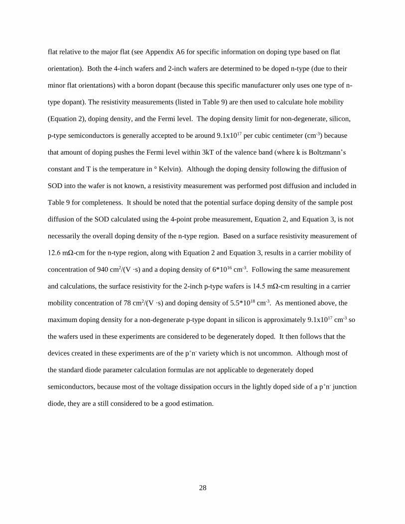
flat relative to the major flat (see Appendix A6 for specific information on doping type based on flat
orientation). Both the 4-inch wafers and 2-inch wafers are determined to be doped n-type (due to their
minor flat orientations) with a boron dopant (because this specific manufacturer only uses one type of n-
type dopant). The resistivity measurements (listed in Table 9) are then used to calculate hole mobility
(Equation 2), doping density, and the Fermi level. The doping density limit for non-degenerate, silicon,
p-type semiconductors is generally accepted to be around 9.1x10¹⁷ per cubic centimeter (cm-3) because
that amount of doping pushes the Fermi level within 3kT of the valence band (where k is Boltzmann’s
constant and T is the temperature in ° Kelvin). Although the doping density following the diffusion of
SOD into the wafer is not known, a resistivity measurement was performed post diffusion and included in
Table 9 for completeness. It should be noted that the potential surface doping density of the sample post
diffusion of the SOD calculated using the 4-point probe measurement, Equation 2, and Equation 3, is not
necessarily the overall doping density of the n-type region. Based on a surface resistivity measurement of
12.6 mΩ-cm for the n-type region, along with Equation 2 and Equation 3, results in a carrier mobility of
concentration of 940 cm2/(V ·s) and a doping density of 6*1016 cm-3. Following the same measurement
and calculations, the surface resistivity for the 2-inch p-type wafers is 14.5 mΩ-cm resulting in a carrier
mobility concentration of 78 cm2/(V ·s) and doping density of 5.5*1018 cm-3. As mentioned above, the
maximum doping density for a non-degenerate p-type dopant in silicon is approximately 9.1x1017 cm-3 so
the wafers used in these experiments are considered to be degenerately doped. It then follows that the
devices created in these experiments are of the p+n- variety which is not uncommon. Although most of
the standard diode parameter calculation formulas are not applicable to degenerately doped
semiconductors, because most of the voltage dissipation occurs in the lightly doped side of a p+n- junction
diode, they are a still considered to be a good estimation.
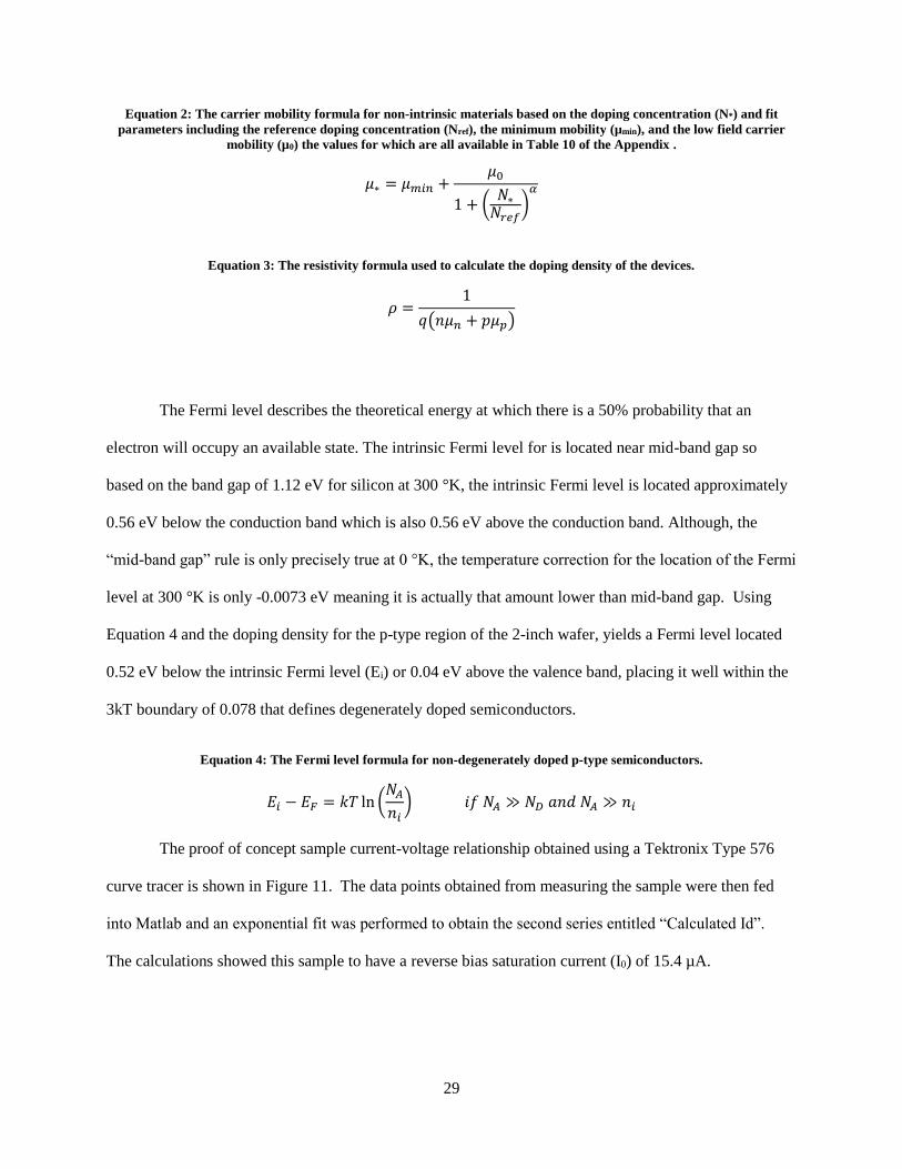
29
Equation 2: The carrier mobility formula for non-intrinsic materials based on the doping concentration (N*) and fit
parameters including the reference doping concentration (Nref), the minimum mobility (µmin), and the low field carrier
mobility (µ0) the values for which are all available in Table 10 of the Appendix .
𝜇∗ = 𝜇𝑚𝑖𝑛 +𝜇0
1 + (𝑁∗
𝑁𝑟𝑒𝑓)
𝛼
Equation 3: The resistivity formula used to calculate the doping density of the devices.
𝜌 =1
𝑞(𝑛𝜇𝑛 + 𝑝𝜇𝑝)
The Fermi level describes the theoretical energy at which there is a 50% probability that an
electron will occupy an available state. The intrinsic Fermi level for is located near mid-band gap so
based on the band gap of 1.12 eV for silicon at 300 °K, the intrinsic Fermi level is located approximately
0.56 eV below the conduction band which is also 0.56 eV above the conduction band. Although, the
“mid-band gap” rule is only precisely true at 0 °K, the temperature correction for the location of the Fermi
level at 300 °K is only -0.0073 eV meaning it is actually that amount lower than mid-band gap. Using
Equation 4 and the doping density for the p-type region of the 2-inch wafer, yields a Fermi level located
0.52 eV below the intrinsic Fermi level (Ei) or 0.04 eV above the valence band, placing it well within the
3kT boundary of 0.078 that defines degenerately doped semiconductors.
Equation 4: The Fermi level formula for non-degenerately doped p-type semiconductors.
𝐸𝑖 − 𝐸𝐹 = 𝑘𝑇 ln (𝑁𝐴
𝑛𝑖) 𝑖𝑓 𝑁𝐴 ≫ 𝑁𝐷 𝑎𝑛𝑑 𝑁𝐴 ≫ 𝑛𝑖
The proof of concept sample current-voltage relationship obtained using a Tektronix Type 576
curve tracer is shown in Figure 11. The data points obtained from measuring the sample were then fed
into Matlab and an exponential fit was performed to obtain the second series entitled “Calculated Id”.
The calculations showed this sample to have a reverse bias saturation current (I0) of 15.4 µA.
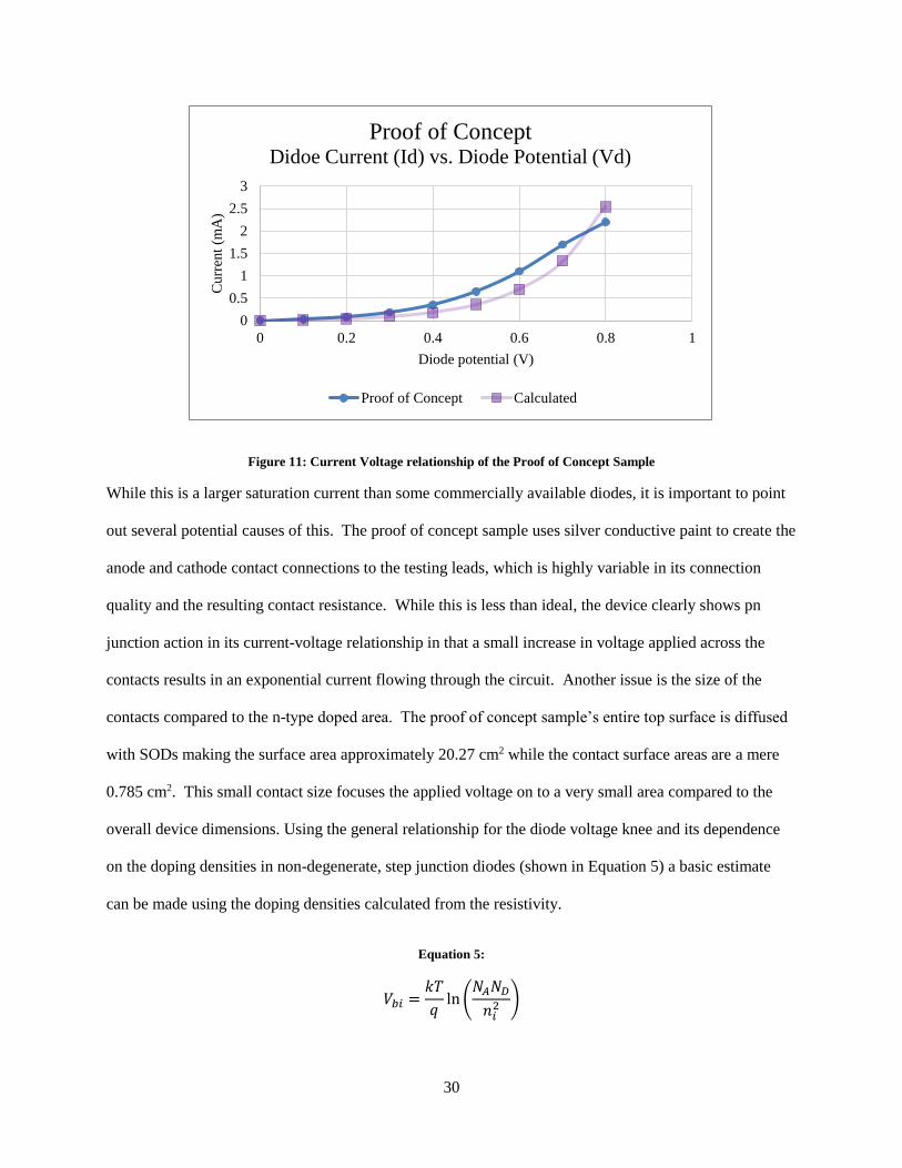
30
Figure 11: Current Voltage relationship of the Proof of Concept Sample
While this is a larger saturation current than some commercially available diodes, it is important to point
out several potential causes of this. The proof of concept sample uses silver conductive paint to create the
anode and cathode contact connections to the testing leads, which is highly variable in its connection
quality and the resulting contact resistance. While this is less than ideal, the device clearly shows pn
junction action in its current-voltage relationship in that a small increase in voltage applied across the
contacts results in an exponential current flowing through the circuit. Another issue is the size of the
contacts compared to the n-type doped area. The proof of concept sample’s entire top surface is diffused
with SODs making the surface area approximately 20.27 cm2 while the contact surface areas are a mere
0.785 cm2. This small contact size focuses the applied voltage on to a very small area compared to the
overall device dimensions. Using the general relationship for the diode voltage knee and its dependence
on the doping densities in non-degenerate, step junction diodes (shown in Equation 5) a basic estimate
can be made using the doping densities calculated from the resistivity.
Equation 5:
𝑉𝑏𝑖 =𝑘𝑇
𝑞ln (
𝑁𝐴𝑁𝐷
𝑛𝑖2 )
0
0.5
1
1.5
2
2.5
3
0 0.2 0.4 0.6 0.8 1
Curr
ent
(mA
)
Diode potential (V)
Proof of ConceptDidoe Current (Id) vs. Diode Potential (Vd)
Proof of Concept Calculated

31
When using the constants shown in Table 9 and the estimated doping parameters in Table 10, the proof of
concept sample’s estimated voltage knee is 0.925 volts. This is a reasonable estimation given that the
intrinsic band gap of silicon is 1.12 eV and the sample’s I-V characteristics. The deviation of the
sample’s measured current from the calculated values at higher voltages is most likely due to the added
series resistance of the contacts.
Section 4.2: Contact Comparison
The next sample to be analyzed is the contact comparison sample. For this sample, the contact
for the cathode is placed only on the top surface while contacts for the anode are placed on both the top
side and bottom side of the wafer. The contact comparison sample is tested using the same procedures
used for the proof of concept sample in the preceding paragraphs. Although the experimental procedure
is presented to create only one device, three devices were created to increase the amount of data obtained
from testing and to ensure quality of data in that all samples presented the same results. The resulting I-V
curves are shown below in Figure 12 and Figure 13. Figure 12 shows that the same voltage applied
across the top contacts results in a much larger diode current than when applied across the top and bottom
contacts. One reason for this is due to the contact resistance. Though the contacts were created in an
identical fashion, the bottom contact is deposited onto the unpolished bottom surface of the wafer. The
polished top plane of the creates a clean bonding surface for the contacts and creates a better electrical
connection. Due to the drastic difference in the resulting diode currents, the semi-log graph of currents
(Figure 13) was also included in order to better illustrate the two I-V relationships on the same chart even
though their values are magnitudes apart. Another potential cause of the relatively poor performance of
the bottom contact is the short diffusion profile used when creating this sample. If the shorter diffusion
profile does not allow the SOD to diffuse far enough into the substrate, the highly doped p+ side of the
junction could be very large compared to the lighter doped n- side. Since most of the voltage dissipation
occurs in the quasi-neutral region, this imbalance would cause a disproportionate carrier density in the p-
type material due to the physically large size compared to that of the n-type material. The metallurgical
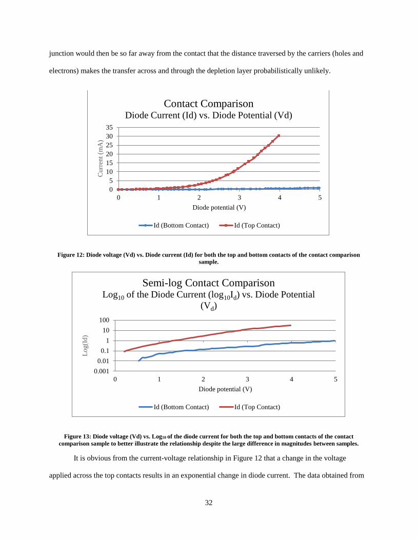
32
junction would then be so far away from the contact that the distance traversed by the carriers (holes and
electrons) makes the transfer across and through the depletion layer probabilistically unlikely.
Figure 12: Diode voltage (Vd) vs. Diode current (Id) for both the top and bottom contacts of the contact comparison
sample.
Figure 13: Diode voltage (Vd) vs. Log10 of the diode current for both the top and bottom contacts of the contact
comparison sample to better illustrate the relationship despite the large difference in magnitudes between samples.
It is obvious from the current-voltage relationship in Figure 12 that a change in the voltage
applied across the top contacts results in an exponential change in diode current. The data obtained from
0
5
10
15
20
25
30
35
0 1 2 3 4 5
Curr
ent
(mA
)
Diode potential (V)
Contact ComparisonDiode Current (Id) vs. Diode Potential (Vd)
Id (Bottom Contact) Id (Top Contact)
0.001
0.01
0.1
1
10
100
0 1 2 3 4 5
Lo
g(I
d)
Diode potential (V)
Semi-log Contact ComparisonLog10 of the Diode Current (log10Id) vs. Diode Potential
(Vd)
Id (Bottom Contact) Id (Top Contact)
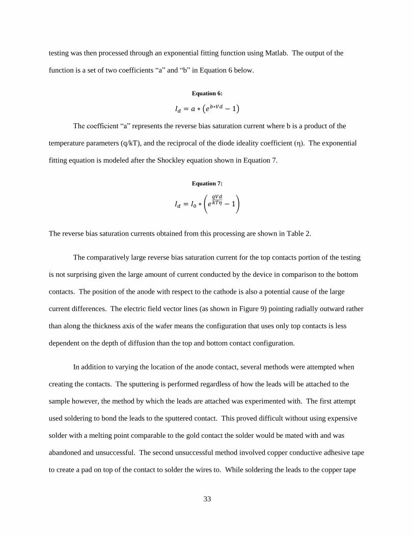
33
testing was then processed through an exponential fitting function using Matlab. The output of the
function is a set of two coefficients “a” and “b” in Equation 6 below.
Equation 6:
𝐼𝑑 = 𝑎 ∗ (𝑒𝑏∗𝑉𝑑 − 1)
The coefficient “a” represents the reverse bias saturation current where b is a product of the
temperature parameters (q/kT), and the reciprocal of the diode ideality coefficient (η). The exponential
fitting equation is modeled after the Shockley equation shown in Equation 7.
Equation 7:
𝐼𝑑 = 𝐼0 ∗ (𝑒𝑞𝑉𝑑𝑘𝑇𝜂 − 1)
The reverse bias saturation currents obtained from this processing are shown in Table 2.
The comparatively large reverse bias saturation current for the top contacts portion of the testing
is not surprising given the large amount of current conducted by the device in comparison to the bottom
contacts. The position of the anode with respect to the cathode is also a potential cause of the large
current differences. The electric field vector lines (as shown in Figure 9) pointing radially outward rather
than along the thickness axis of the wafer means the configuration that uses only top contacts is less
dependent on the depth of diffusion than the top and bottom contact configuration.
In addition to varying the location of the anode contact, several methods were attempted when
creating the contacts. The sputtering is performed regardless of how the leads will be attached to the
sample however, the method by which the leads are attached was experimented with. The first attempt
used soldering to bond the leads to the sputtered contact. This proved difficult without using expensive
solder with a melting point comparable to the gold contact the solder would be mated with and was
abandoned and unsuccessful. The second unsuccessful method involved copper conductive adhesive tape
to create a pad on top of the contact to solder the wires to. While soldering the leads to the copper tape
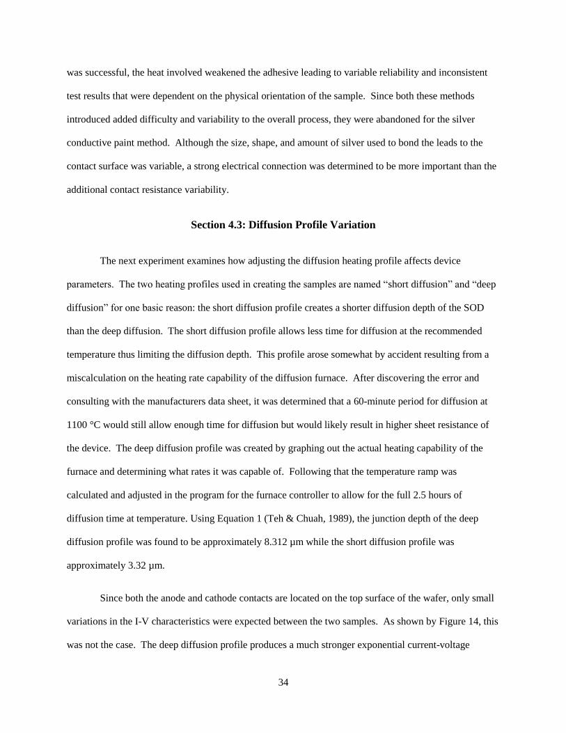
34
was successful, the heat involved weakened the adhesive leading to variable reliability and inconsistent
test results that were dependent on the physical orientation of the sample. Since both these methods
introduced added difficulty and variability to the overall process, they were abandoned for the silver
conductive paint method. Although the size, shape, and amount of silver used to bond the leads to the
contact surface was variable, a strong electrical connection was determined to be more important than the
additional contact resistance variability.
Section 4.3: Diffusion Profile Variation
The next experiment examines how adjusting the diffusion heating profile affects device
parameters. The two heating profiles used in creating the samples are named “short diffusion” and “deep
diffusion” for one basic reason: the short diffusion profile creates a shorter diffusion depth of the SOD
than the deep diffusion. The short diffusion profile allows less time for diffusion at the recommended
temperature thus limiting the diffusion depth. This profile arose somewhat by accident resulting from a
miscalculation on the heating rate capability of the diffusion furnace. After discovering the error and
consulting with the manufacturers data sheet, it was determined that a 60-minute period for diffusion at
1100 °C would still allow enough time for diffusion but would likely result in higher sheet resistance of
the device. The deep diffusion profile was created by graphing out the actual heating capability of the
furnace and determining what rates it was capable of. Following that the temperature ramp was
calculated and adjusted in the program for the furnace controller to allow for the full 2.5 hours of
diffusion time at temperature. Using Equation 1 (Teh & Chuah, 1989), the junction depth of the deep
diffusion profile was found to be approximately 8.312 µm while the short diffusion profile was
approximately 3.32 µm.
Since both the anode and cathode contacts are located on the top surface of the wafer, only small
variations in the I-V characteristics were expected between the two samples. As shown by Figure 14, this
was not the case. The deep diffusion profile produces a much stronger exponential current-voltage
35
relationship than the short diffusion profile. One cause of this is the number of majority carriers
participating in the transfer across the depletion layer. The deeper diffusion allows for more phosphorus
atoms to penetrate into the material creating a larger n-type area populated with more carriers.
Figure 14: This graph compares the I-V characteristics of the deep diffusion heating profile to those of the short diffusion
profile's.
Additionally, the longer diffusion time leads to lower sheet resistance as stated by the
manufacturer data sheet. The higher sheet resistance of the short diffusion sample shifts the voltage knee
to a higher voltage because the some of the applied voltage is dissipated by the sheet resistance before it
reaches the p-type portion of the wafer. Similarly, since it is the potential difference between the anode
and cathode that causes the migration of the majority carriers, any potential dissipated by the sheet
resistance between the cathode contact and the n-type region subtract from that which is present between
the materials. The sheet resistance, the contact resistance, and the resistance of the silver paint used to
connect the wires to the contacts act as a series resistance to the diode and are equivalent to adding a load
to the circuit. This is series loading is represented by Rseries1 and Rseries2 in Figure 15.
0
25
50
75
100
125
150
0 0.5 1 1.5 2 2.5 3
Curr
ent
(mA
)
Diode potential (V)
Diffusion Profile ComparisonDiode Current vs. Diode Potential
Deep Diffusion Profile Short Diffusion Profile
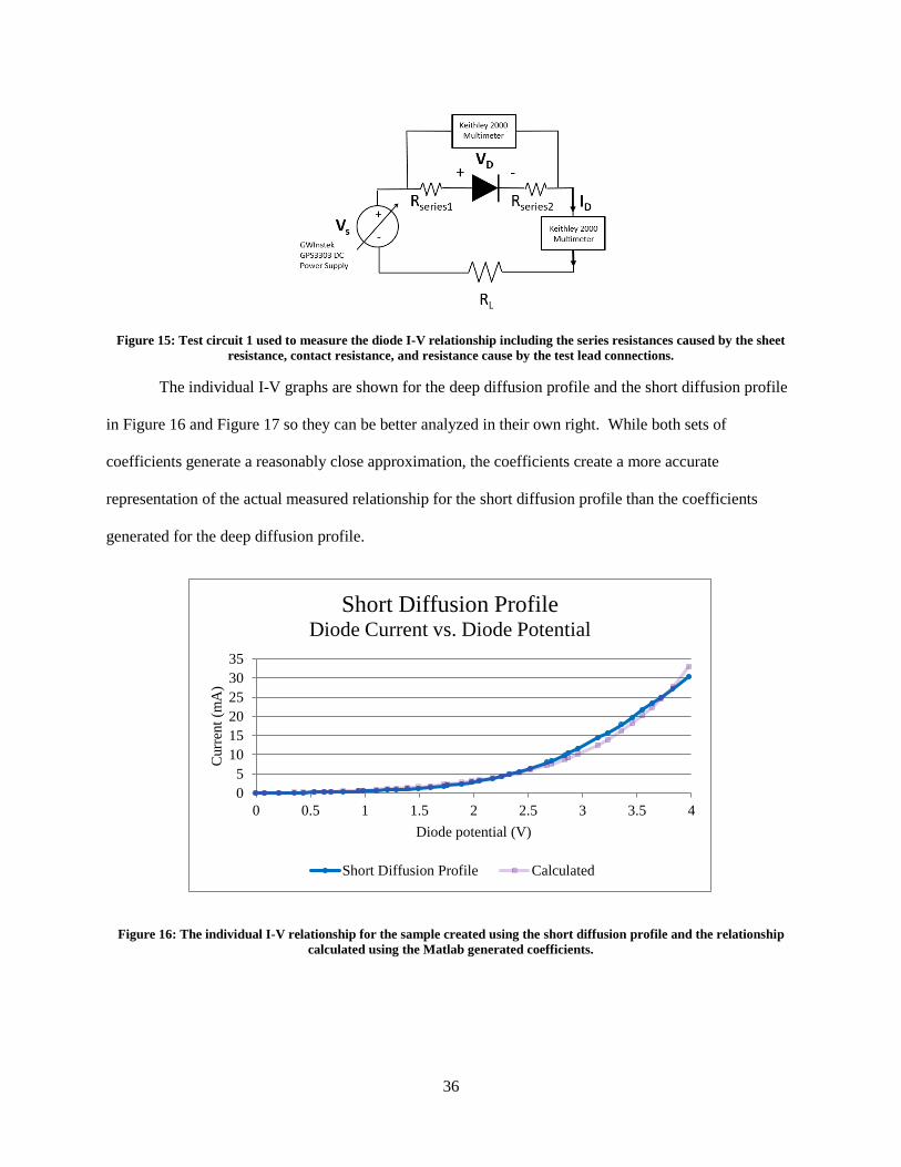
36
Figure 15: Test circuit 1 used to measure the diode I-V relationship including the series resistances caused by the sheet
resistance, contact resistance, and resistance cause by the test lead connections.
The individual I-V graphs are shown for the deep diffusion profile and the short diffusion profile
in Figure 16 and Figure 17 so they can be better analyzed in their own right. While both sets of
coefficients generate a reasonably close approximation, the coefficients create a more accurate
representation of the actual measured relationship for the short diffusion profile than the coefficients
generated for the deep diffusion profile.
Figure 16: The individual I-V relationship for the sample created using the short diffusion profile and the relationship
calculated using the Matlab generated coefficients.
0
5
10
15
20
25
30
35
0 0.5 1 1.5 2 2.5 3 3.5 4
Curr
ent
(mA
)
Diode potential (V)
Short Diffusion ProfileDiode Current vs. Diode Potential
Short Diffusion Profile Calculated
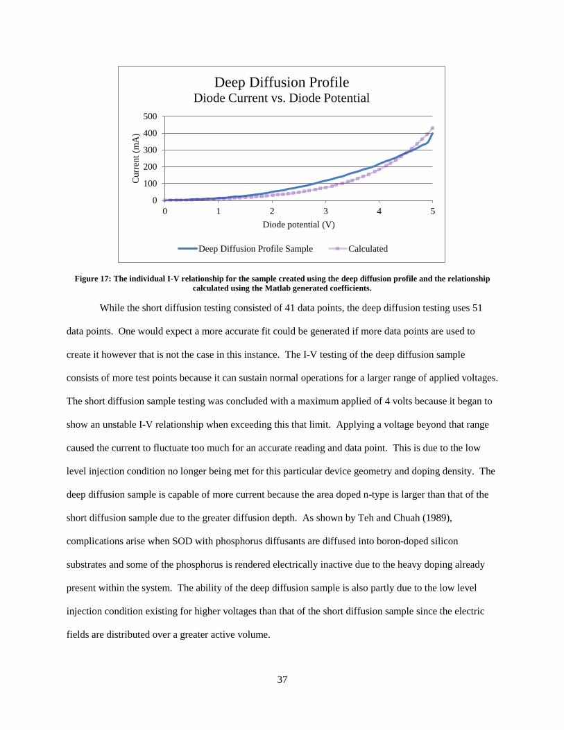
37
Figure 17: The individual I-V relationship for the sample created using the deep diffusion profile and the relationship
calculated using the Matlab generated coefficients.
While the short diffusion testing consisted of 41 data points, the deep diffusion testing uses 51
data points. One would expect a more accurate fit could be generated if more data points are used to
create it however that is not the case in this instance. The I-V testing of the deep diffusion sample
consists of more test points because it can sustain normal operations for a larger range of applied voltages.
The short diffusion sample testing was concluded with a maximum applied of 4 volts because it began to
show an unstable I-V relationship when exceeding this that limit. Applying a voltage beyond that range
caused the current to fluctuate too much for an accurate reading and data point. This is due to the low
level injection condition no longer being met for this particular device geometry and doping density. The
deep diffusion sample is capable of more current because the area doped n-type is larger than that of the
short diffusion sample due to the greater diffusion depth. As shown by Teh and Chuah (1989),
complications arise when SOD with phosphorus diffusants are diffused into boron-doped silicon
substrates and some of the phosphorus is rendered electrically inactive due to the heavy doping already
present within the system. The ability of the deep diffusion sample is also partly due to the low level
injection condition existing for higher voltages than that of the short diffusion sample since the electric
fields are distributed over a greater active volume.
0
100
200
300
400
500
0 1 2 3 4 5
Curr
ent
(mA
)
Diode potential (V)
Deep Diffusion ProfileDiode Current vs. Diode Potential
Deep Diffusion Profile Sample Calculated
38
The voltage knee of both samples is pushed beyond that of the theoretical 0.925 volts for which
there are several explanations. The first was shown when testing the proof of concept sample in which it
was due to the large contact resistance created by both the sputtering procedure and the silver conductive
paint used to secure the leads to the contacts. The second is a result of the method used to deposit the
SOD onto the wafer. As stated by Teh and Chuah (1989) and in the manufacturer data sheet for the SOD,
the SOD shows superior diffusion when deposited and spun in an environment with around 30% relative
humidity. Additionally, both recommend the SOD be diffused in a non-oxidizing atmosphere comprised
of mostly nitrogen. Since this is not possible for the lab the cleanroom facility at UNLV, these two
samples used an oxygen atmosphere for the drive-in/diffusion bake. The increased oxygenation leads to
lower rates of diffusion and higher material resistivity. In order to lower the voltage knee closer to the
theoretical value a nitrogen source and injection valve would need to be added to the lithography room
within the cleanroom and connected to the diffusion furnace. The samples were also not deposited in
30% relative humidity, since the spin coater used lacks temperature and humidity control, the SOD was
applied in around 10% relative humidity at approximately 80 °C because those were the conditions of the
photolithography room during this process. Since the SOD was not deposited or diffused in optimum
conditions it follows that the quality of diffusion is also not optimum. Though the conditions were not
ideal, Figure 16 and Figure 17 demonstrate there is still pn junction action occurring within the material
systems.
Section 4.4: Process Variation
The process variation samples compare the manufacturer recommended process to the process
developed during the experimental portion of this research. The manufacturer recommends depositing the
SOD first then using the polymerization of the photoresist to protect it from dissolving the SOD over the
n-well region during the removal of the rest of it. The process developed for this research uses the diffuse
through photoresist method in which the photoresist is deposited first then the SOD is diffused into the
desired areas through windows opened in the photoresist using photolithography. The manufacturer
39
recommended procedure provide extremely difficult due to the strength of the buffered HF used to
remove the SOD from the areas to remain p-type. After 3 attempts to remove only the undesired SOD
from the wafer, it was determined that the buffering agent (ammonium fluoride, NH4F) was seven years
beyond its expiration date and was not reducing the acidity of the HF enough to allow the polymerized
photoresist to protect the SOD in the diffusion areas. To solve this issue, the HF was combined with twice
as much deionized water as originally required. This only somewhat succeeded in reducing the
concentration of the HF but the desired n-well dimensions were not achieved due over etching. It is
suspected that using a non-expired buffering agent would make this process more viable. Additionally,
the developer used to remove the photoresist from the undesired areas of the sample also washed away
the SOD in those areas. This does not affect process because those areas required clearing of the SOD
anyway however it is suspected that some of the SOD from the areas where the diffusant is required. The
cause of this is most likely the humidity of the room where the SOD is applied being too low leading to
poor adhesion between the SOD and the surface of the wafer.
In Figure 18, the current-voltage relationships for both processes are shown. It is apparent that
diffusing the SOD through the photoresist produced a better device because it has a stronger exponential
relationship and conducts more current than that of the device fabricated using the manufacturer
recommended process. The Diffuse through photoresist sample showed a maximum current of 30.35 mA
for an applied voltage of 3.98 V while the sample created using the manufacturer recommended reached a
maximum of 5.67 mA for an applied voltage of 4.07 V.
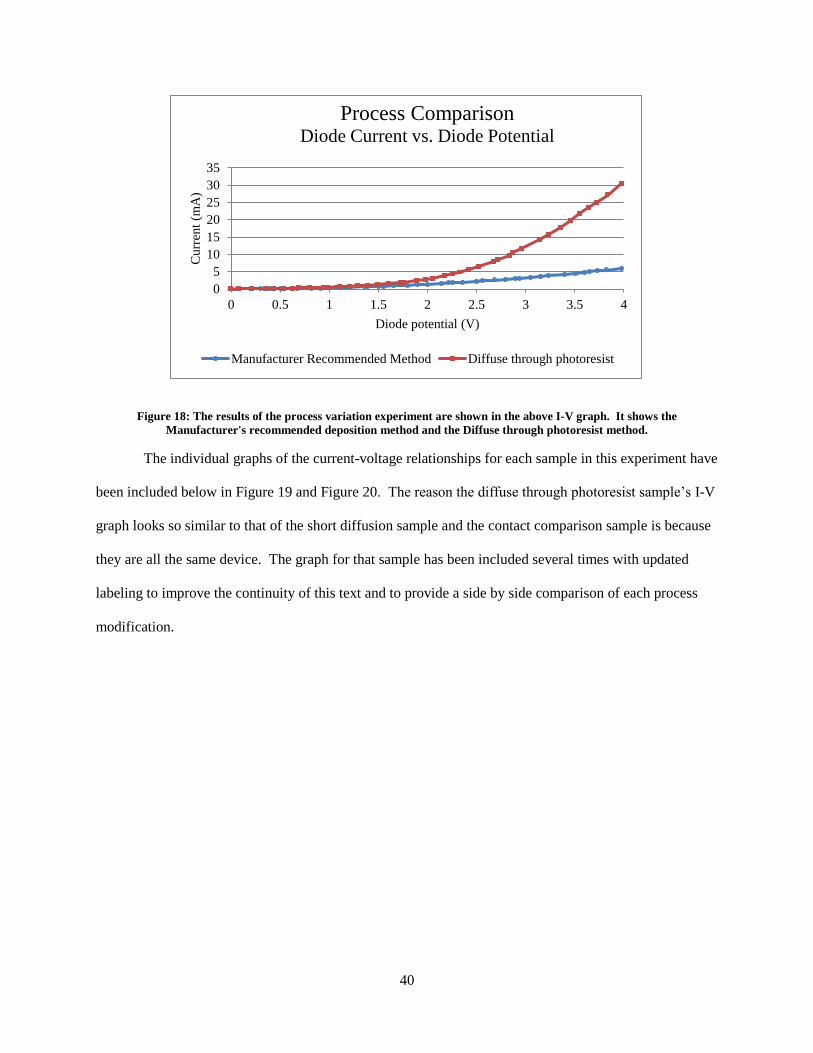
40
Figure 18: The results of the process variation experiment are shown in the above I-V graph. It shows the
Manufacturer's recommended deposition method and the Diffuse through photoresist method.
The individual graphs of the current-voltage relationships for each sample in this experiment have
been included below in Figure 19 and Figure 20. The reason the diffuse through photoresist sample’s I-V
graph looks so similar to that of the short diffusion sample and the contact comparison sample is because
they are all the same device. The graph for that sample has been included several times with updated
labeling to improve the continuity of this text and to provide a side by side comparison of each process
modification.
0
5
10
15
20
25
30
35
0 0.5 1 1.5 2 2.5 3 3.5 4
Curr
ent
(mA
)
Diode potential (V)
Process ComparisonDiode Current vs. Diode Potential
Manufacturer Recommended Method Diffuse through photoresist
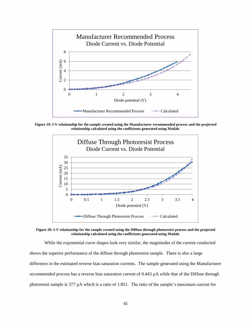
41
Figure 19: I-V relationship for the sample created using the Manufacturer recommended process and the projected
relationship calculated using the coefficients generated using Matlab.
Figure 20: I-V relationship for the sample created using the Diffuse through photoresist process and the projected
relationship calculated using the coefficients generated using Matlab.
While the exponential curve shapes look very similar, the magnitudes of the current conducted
shows the superior performance of the diffuse through photoresist sample. There is also a large
difference in the estimated reverse bias saturation currents. The sample generated using the Manufacturer
recommended process has a reverse bias saturation current of 0.443 µA while that of the Diffuse through
photoresist sample is 377 µA which is a ratio of 1:851. The ratio of the sample’s maximum current for
0
2
4
6
8
0 1 2 3 4
Curr
ent
(mA
)
Diode potential (V)
Manufacturer Recommended ProcessDiode Current vs. Diode Potential
Manufacturer Recommended Process Calculated
0
5
10
15
20
25
30
35
0 0.5 1 1.5 2 2.5 3 3.5 4
Curr
ent
(mA
)
Diode potential (V)
Diffuse Through Photoresist ProcessDiode Current vs. Diode Potential
Diffuse Through Photoresist Process Calculated
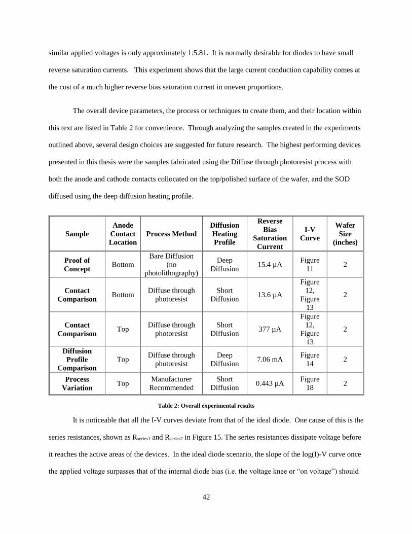
42
similar applied voltages is only approximately 1:5.81. It is normally desirable for diodes to have small
reverse saturation currents. This experiment shows that the large current conduction capability comes at
the cost of a much higher reverse bias saturation current in uneven proportions.
The overall device parameters, the process or techniques to create them, and their location within
this text are listed in Table 2 for convenience. Through analyzing the samples created in the experiments
outlined above, several design choices are suggested for future research. The highest performing devices
presented in this thesis were the samples fabricated using the Diffuse through photoresist process with
both the anode and cathode contacts collocated on the top/polished surface of the wafer, and the SOD
diffused using the deep diffusion heating profile.
Sample
Anode
Contact
Location
Process Method
Diffusion
Heating
Profile
Reverse
Bias
Saturation
Current
I-V
Curve
Wafer
Size
(inches)
Proof of
Concept Bottom
Bare Diffusion
(no
photolithography)
Deep
Diffusion 15.4 µA
Figure
11 2
Contact
Comparison Bottom
Diffuse through
photoresist
Short
Diffusion 13.6 µA
Figure
12,
Figure
13
2
Contact
Comparison Top
Diffuse through
photoresist
Short
Diffusion 377 µA
Figure
12,
Figure
13
2
Diffusion
Profile
Comparison
Top Diffuse through
photoresist
Deep
Diffusion 7.06 mA
Figure
14 2
Process
Variation Top
Manufacturer
Recommended
Short
Diffusion 0.443 µA
Figure
18 2
Table 2: Overall experimental results
It is noticeable that all the I-V curves deviate from that of the ideal diode. One cause of this is the
series resistances, shown as Rseries1 and Rseries2 in Figure 15. The series resistances dissipate voltage before
it reaches the active areas of the devices. In the ideal diode scenario, the slope of the log(I)-V curve once
the applied voltage surpasses that of the internal diode bias (i.e. the voltage knee or “on voltage”) should
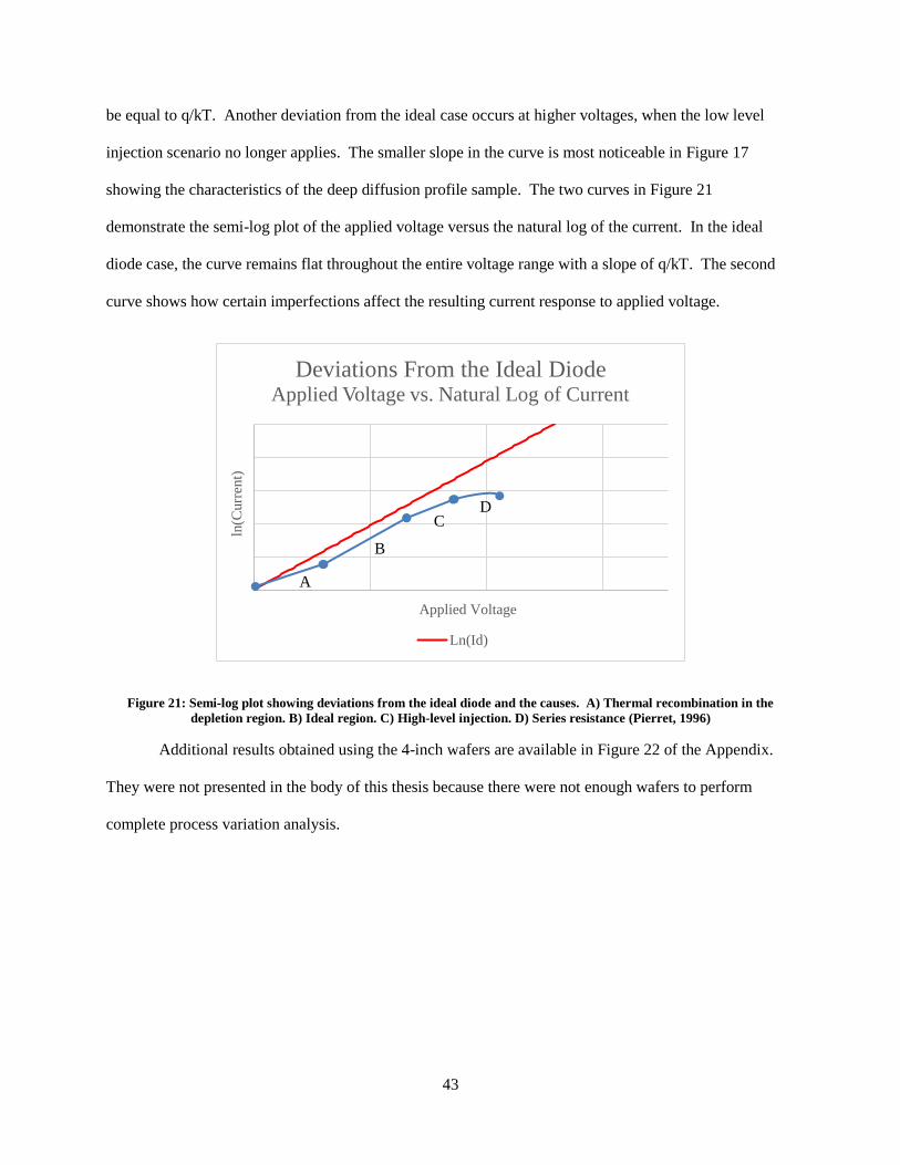
43
be equal to q/kT. Another deviation from the ideal case occurs at higher voltages, when the low level
injection scenario no longer applies. The smaller slope in the curve is most noticeable in Figure 17
showing the characteristics of the deep diffusion profile sample. The two curves in Figure 21
demonstrate the semi-log plot of the applied voltage versus the natural log of the current. In the ideal
diode case, the curve remains flat throughout the entire voltage range with a slope of q/kT. The second
curve shows how certain imperfections affect the resulting current response to applied voltage.
Figure 21: Semi-log plot showing deviations from the ideal diode and the causes. A) Thermal recombination in the
depletion region. B) Ideal region. C) High-level injection. D) Series resistance (Pierret, 1996)
Additional results obtained using the 4-inch wafers are available in Figure 22 of the Appendix.
They were not presented in the body of this thesis because there were not enough wafers to perform
complete process variation analysis.
ln(C
urr
ent)
Applied Voltage
Deviations From the Ideal DiodeApplied Voltage vs. Natural Log of Current
Ln(Id)
A
B
C D
44
Chapter 5: Conclusion
Throughout this work, several methods and processes to design, fabricate and test semiconductor
devices are presented. Based on the results included above, the process provided is successful in that it
results in functioning pn junction diodes. Only equipment and materials deemed absolutely necessary were
used in these experiments to allow facilities with less developed semiconductor device programs to recreate
them with little to no additional equipment. While the device manufacturer suggests using a specialty
spinner for SOD application, the standard photoresist spinning equipment was used instead to avoid extra
cost. Additionally, rather than using an electron beam physical vapor deposition system to deposit the metal
for the device contacts, the much less expensive SPI Sputtering system was used. In addition to the lower
price of the SPI system, it also requires much less training to operate as well as less infrastructure to support
it.
During the early stages of research, the manufacturer’s recommended conditions were followed as
closely as possible however this made the process far more difficult, complicated, and variable than needed.
One example of this is the suggestion to deposit the SOD onto the wafers surface as the first step in the
process. The major difficulty encountered when following these instructions was that the polymerized
photoresist rarely prevented all of the SOD from being dissolved during the HF soak to remove the SOD
from the areas aside from the n-well before diffusion. One potential cause for this could be that the
buffering agent (ammonium fluoride) used was seven years beyond its expiration date causing the acidity
in the mixture to be too high. If the acidity is too high, the photoresist will be dissolved regardless of the
level to which it has polymerized. Although this is standard, the test devices created showed better
performance using a much simpler method. The difficulty added by following the manufacturer
recommended process in addition to the results achieved by the diffuse through photoresist method
developed during the experimentation process, yielded much better results.
45
An undesirable characteristic present in all the device samples fabricated in this thesis is the large
potential difference required to “turn on” the diodes. As stated in the Results and Analysis section, a major
cause of this is the abnormally high (and variable) contact resistance resulting from the silver conducting
paint used to secure the test leads to the anode and cathode. A much more consistent and effective method
of securing the test leads to the devices is bonding. The bonding process uses heat and ultrasonic energy
to maximize the reliability and consistency of the connections between the wire and the pad or contact.
Normally a pad would first need to be secured to the connection surface to perform the bonding process
however, since the devices created for this thesis use gold contacts as the base for connections, a pad would
not be required. Although the UNLV cleanroom facility is in possession of a Kulicke & Soffa 4129
Automatic Bonding machine with ultrasonic capability and a Manual Ball Bonder 4522 of the same
manufacturer, both were unavailable for use at the time of this thesis. Once one or both of these machines
become available for use and is used to bond the contacts to the test leads, I expect much more consistent
devices and results.
Through many cycles of trial and error, the least dangerous and time consuming methods resulted
in the best performing devices. For example, the Manufacturer Recommended process was difficult to
perform and required 3 separate buffered HF soaks while the Diffuse through photoresist method only
requires 2. The first soak for both methods is to clean the wafer, the second only applies the manufacturer
recommended process and is to remove the excess SOD, while the third to remove the SOD and oxides
resulting from the diffusion bake post diffusion also applies to both methods. HF is an extremely caustic
and dangerous chemical so it benefits the students and professors who will be performing this lab to handle
it as little as possible. While the samples in which the SOD were diffused using the deep diffusion heating
profile outperformed those using the short diffusion profile in terms of total current conduction, the short
diffusion samples showed lower estimations of for the reverse saturation bias currents with the exception
of the bottom contact testing. If one is in need of a higher power device, the deep diffusion heating profile
should be used to diffuse the SOD because those devices showed higher current output due to the larger
46
number of majority carriers available to the conduction band. In contrast, if a rectifier circuit is the goal,
the Short diffusion profile should be used due to the low reverse bias saturation current of the devices
created using that profile. While the short diffusion profile takes less time than the deep diffusion profile
(1 hour 15 minutes less), both profiles require at least 10 hours to complete fully (including the preheat, the
drive in bake portion, and the cool down). This may seem daunting but because the diffusion furnace has
a temperature controller based on time, the person making the devices only need to be near the oven to
input the profile parameters at the beginning and once it reaches the preheat temperature to insert the
sample. Because of this, using the deep diffusion heating profile requires extra time to complete, but not
extra effort by the fabricator. The coplanar location of the contacts also required less effort than the split
configuration (cathode on the top surface and anode on the bottom) due to the sputtering process. When
collocating the contacts, both are sputtered onto the top surface of the wafer during the same sputtering
session. Transferring the anode contact to the bottom of the wafer requires two sputtering sessions in order
to first expose the top surface to the sputtering head to create the cathode then turning it over and repeating
the process to deposit the anode on the back. Additionally, the split contact configuration requires extra
photolithography steps since the exposure cannot be performed on both surfaces simultaneously. The
devices using the coplanar contact location also showed better performance than those using the split
contact configuration and required less process steps and effort.
One parameter that these experiments failed to address is the temperature of the furnace at the time
of sample was insertion. A relatively unknown technique called rapid thermal processing is starting to
become popularized due to its mass production capability. In this technique, the samples are coated with
SOD and annealed between 900 °C and 950 °C in the range of 10-40 seconds. The contact comparison
sample was inserted into the diffusion furnace at the highest pre-heat temperature of 750 °C while most of
the other samples were inserted from ranges of 250 °C to 500 °C. Future research should include how the
furnace temperature at time of sample insertion affects device parameters.
47
As mentioned in the introduction, this thesis has successfully developed a process to make
semiconductor devices using Spin-On dopants using only the minimum equipment necessary. The devices
created show pn junction characteristics in that the resulting I-V graphs are exponential and follow the same
trends as given by the Shockley equation (Equation 7). All devices show low current conduction for
voltages below the “turn on” threshold which is typical of diodes. Using the process developed for creating
pn junction diodes, interesting experiments to be performed in the future include full and half wave rectifier
circuits, ring oscillators, and simple diode logic circuits. Since the base device in all of these circuits is the
diode, the procedures presented can be modified to produce the circuits with minimal effort. Additional
theoretical information along with the “why” behind each process step is also included in the Lab
Procedures in order to facilitate the “learning by doing” ideology. By reading this paper and implementing
the outlined procedures, the user should be able to reproduce working pn junction diodes.
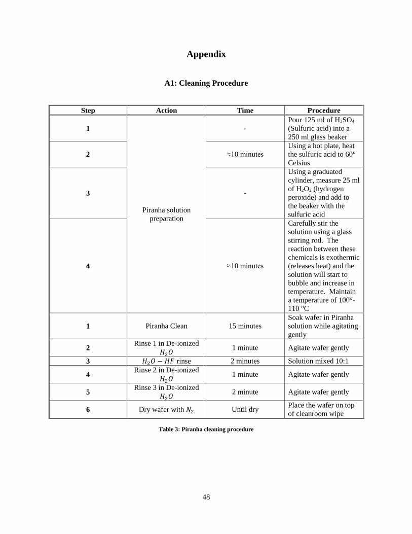
48
Appendix
A1: Cleaning Procedure
Step Action Time Procedure
1
Piranha solution
preparation
-
Pour 125 ml of H2SO4
(Sulfuric acid) into a
250 ml glass beaker
2 ≈10 minutes
Using a hot plate, heat
the sulfuric acid to 60°
Celsius
3 -
Using a graduated
cylinder, measure 25 ml
of H2O2 (hydrogen
peroxide) and add to
the beaker with the
sulfuric acid
4 ≈10 minutes
Carefully stir the
solution using a glass
stirring rod. The
reaction between these
chemicals is exothermic
(releases heat) and the
solution will start to
bubble and increase in
temperature. Maintain
a temperature of 100°-
110 °C
1 Piranha Clean 15 minutes
Soak wafer in Piranha
solution while agitating
gently
2 Rinse 1 in De-ionized
𝐻2𝑂 1 minute Agitate wafer gently
3 𝐻2𝑂 − 𝐻𝐹 rinse 2 minutes Solution mixed 10:1
4 Rinse 2 in De-ionized
𝐻2𝑂 1 minute Agitate wafer gently
5 Rinse 3 in De-ionized
𝐻2𝑂 2 minute Agitate wafer gently
6 Dry wafer with 𝑁2 Until dry Place the wafer on top
of cleanroom wipe
Table 3: Piranha cleaning procedure
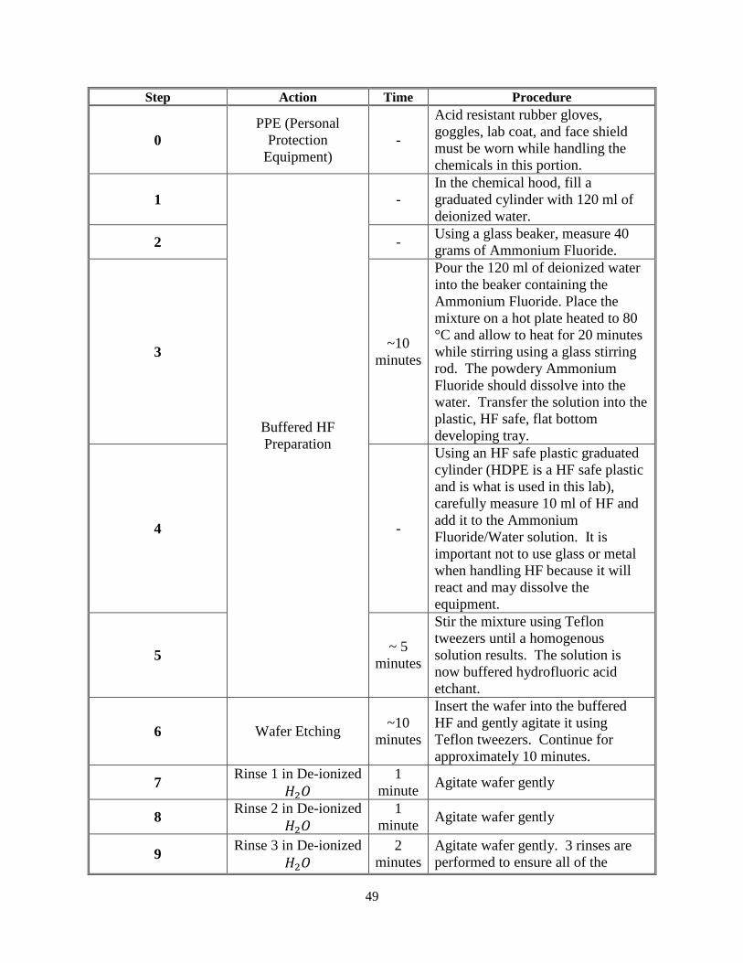
49
Step Action Time Procedure
0
PPE (Personal
Protection
Equipment)
-
Acid resistant rubber gloves,
goggles, lab coat, and face shield
must be worn while handling the
chemicals in this portion.
1
Buffered HF
Preparation
-
In the chemical hood, fill a
graduated cylinder with 120 ml of
deionized water.
2 - Using a glass beaker, measure 40
grams of Ammonium Fluoride.
3 ~10
minutes
Pour the 120 ml of deionized water
into the beaker containing the
Ammonium Fluoride. Place the
mixture on a hot plate heated to 80
°C and allow to heat for 20 minutes
while stirring using a glass stirring
rod. The powdery Ammonium
Fluoride should dissolve into the
water. Transfer the solution into the
plastic, HF safe, flat bottom
developing tray.
4 -
Using an HF safe plastic graduated
cylinder (HDPE is a HF safe plastic
and is what is used in this lab),
carefully measure 10 ml of HF and
add it to the Ammonium
Fluoride/Water solution. It is
important not to use glass or metal
when handling HF because it will
react and may dissolve the
equipment.
5 ~ 5
minutes
Stir the mixture using Teflon
tweezers until a homogenous
solution results. The solution is
now buffered hydrofluoric acid
etchant.
6 Wafer Etching ~10
minutes
Insert the wafer into the buffered
HF and gently agitate it using
Teflon tweezers. Continue for
approximately 10 minutes.
7 Rinse 1 in De-ionized
𝐻2𝑂
1
minute Agitate wafer gently
8 Rinse 2 in De-ionized
𝐻2𝑂
1
minute Agitate wafer gently
9 Rinse 3 in De-ionized
𝐻2𝑂
2
minutes
Agitate wafer gently. 3 rinses are
performed to ensure all of the
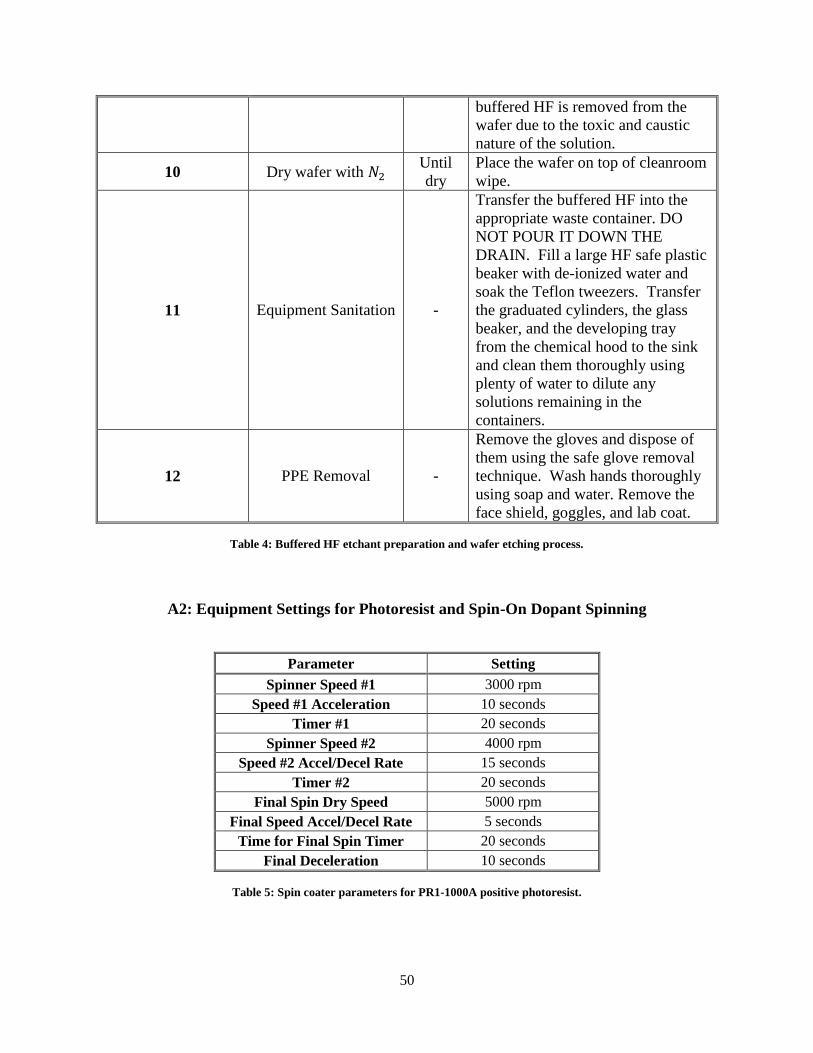
50
buffered HF is removed from the
wafer due to the toxic and caustic
nature of the solution.
10 Dry wafer with 𝑁2 Until
dry
Place the wafer on top of cleanroom
wipe.
11 Equipment Sanitation -
Transfer the buffered HF into the
appropriate waste container. DO
NOT POUR IT DOWN THE
DRAIN. Fill a large HF safe plastic
beaker with de-ionized water and
soak the Teflon tweezers. Transfer
the graduated cylinders, the glass
beaker, and the developing tray
from the chemical hood to the sink
and clean them thoroughly using
plenty of water to dilute any
solutions remaining in the
containers.
12 PPE Removal -
Remove the gloves and dispose of
them using the safe glove removal
technique. Wash hands thoroughly
using soap and water. Remove the
face shield, goggles, and lab coat.
Table 4: Buffered HF etchant preparation and wafer etching process.
A2: Equipment Settings for Photoresist and Spin-On Dopant Spinning
Parameter Setting
Spinner Speed #1 3000 rpm
Speed #1 Acceleration 10 seconds
Timer #1 20 seconds
Spinner Speed #2 4000 rpm
Speed #2 Accel/Decel Rate 15 seconds
Timer #2 20 seconds
Final Spin Dry Speed 5000 rpm
Final Speed Accel/Decel Rate 5 seconds
Time for Final Spin Timer 20 seconds
Final Deceleration 10 seconds
Table 5: Spin coater parameters for PR1-1000A positive photoresist.
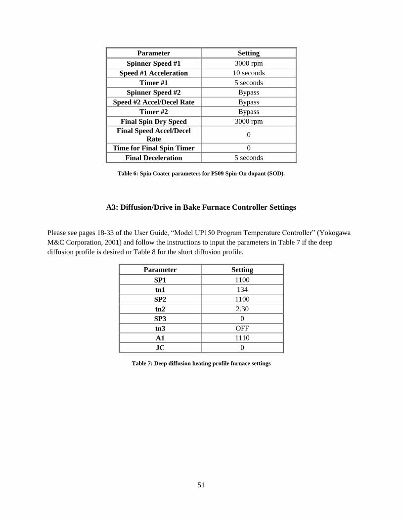
51
Parameter Setting
Spinner Speed #1 3000 rpm
Speed #1 Acceleration 10 seconds
Timer #1 5 seconds
Spinner Speed #2 Bypass
Speed #2 Accel/Decel Rate Bypass
Timer #2 Bypass
Final Spin Dry Speed 3000 rpm
Final Speed Accel/Decel
Rate 0
Time for Final Spin Timer 0
Final Deceleration 5 seconds
Table 6: Spin Coater parameters for P509 Spin-On dopant (SOD).
A3: Diffusion/Drive in Bake Furnace Controller Settings
Please see pages 18-33 of the User Guide, “Model UP150 Program Temperature Controller” (Yokogawa
M&C Corporation, 2001) and follow the instructions to input the parameters in Table 7 if the deep
diffusion profile is desired or Table 8 for the short diffusion profile.
Parameter Setting
SP1 1100
tn1 134
SP2 1100
tn2 2.30
SP3 0
tn3 OFF
A1 1110
JC 0
Table 7: Deep diffusion heating profile furnace settings
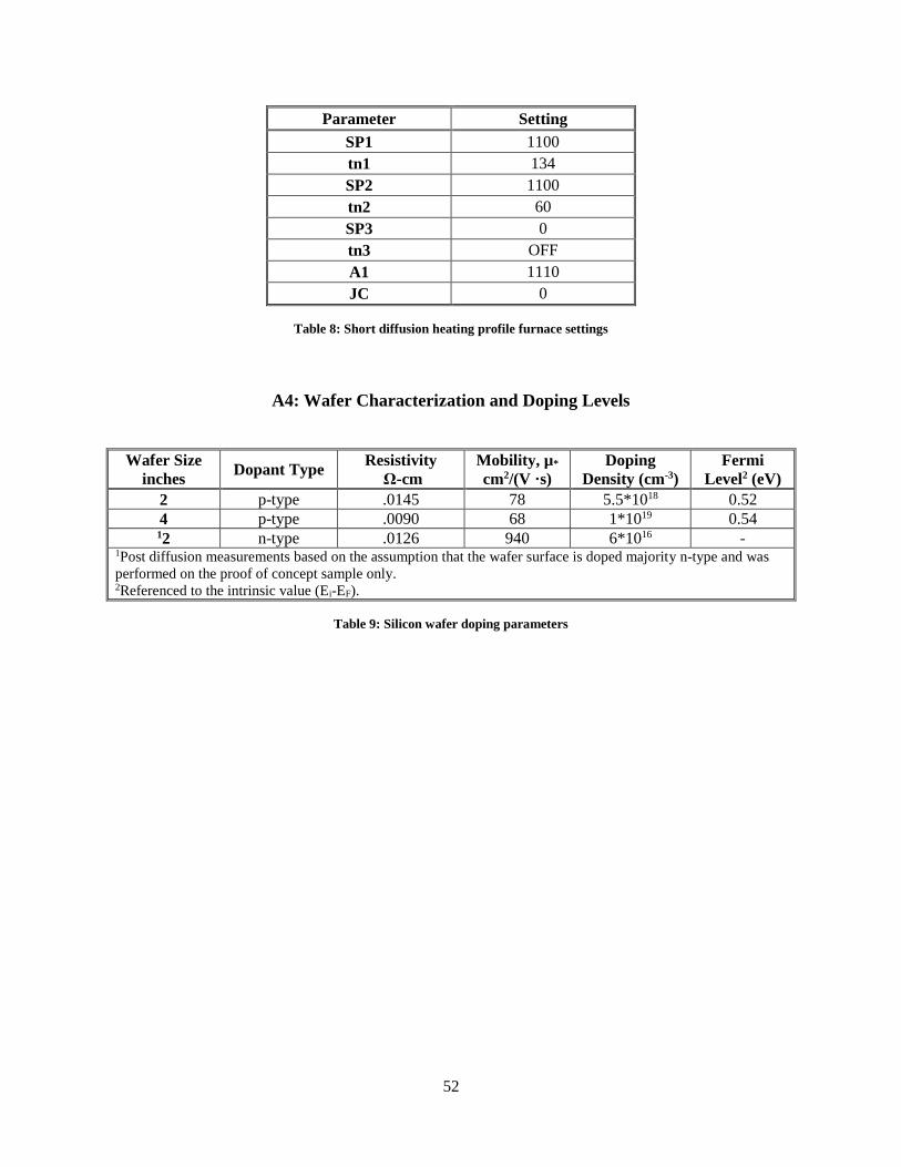
52
Parameter Setting
SP1 1100
tn1 134
SP2 1100
tn2 60
SP3 0
tn3 OFF
A1 1110
JC 0
Table 8: Short diffusion heating profile furnace settings
A4: Wafer Characterization and Doping Levels
Wafer Size
inches Dopant Type
Resistivity
Ω-cm
Mobility, µ*
cm2/(V ·s)
Doping
Density (cm-3)
Fermi
Level2 (eV)
2 p-type .0145 78 5.5*1018 0.52
4 p-type .0090 68 1*1019 0.54 12 n-type .0126 940 6*1016 -
1Post diffusion measurements based on the assumption that the wafer surface is doped majority n-type and was
performed on the proof of concept sample only. 2Referenced to the intrinsic value (Ei-EF).
Table 9: Silicon wafer doping parameters
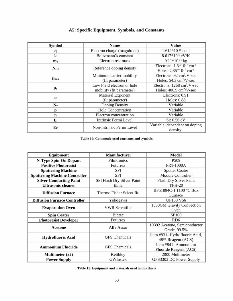
53
A5: Specific Equipment, Symbols, and Constants
Symbol Name Value
q Electron charge (magnitude) 1.612*10-19 coul
k Boltzmann’s constant 8.617*10-5 eV/K
m0 Electron rest mass 9.11*10-31 kg
Nref Reference doping density Electrons: 1.3*1017 cm-3
Holes: 2.35*1017 cm-3
µmin Minimum carrier mobility
(fit parameter)
Electrons: 92 cm2/V-sec
Holes: 54.3 cm2/V-sec
µ0 Low Field electron or hole
mobility (fit parameter)
Electrons: 1268 cm2/V-sec
Holes: 406.9 cm2/V-sec
α Material Exponent
(fit parameter)
Electrons: 0.91
Holes: 0.88
N* Doping Density Variable
p Hole Concentration Variable
n Electron concentration Variable
Ei Intrinsic Fermi Level Si: 0.56 eV
EF Non-Intrinsic Fermi Level Variable, dependent on doping
density.
Table 10: Commonly used constants and symbols
Equipment Manufacturer Model
N-Type Spin-On Dopant Filmtronics P509
Positive Photoresist Futurrex PR1-1000A
Sputtering Machine SPI Sputter Coater
Sputtering Machine Controller SPI Module Controller
Silver Conducting Paint SPI Flash Dry Silver Paint Flash Dry Silver Paint
Ultrasonic cleaner Elma TI-H-20
Diffusion Furnace Thermo Fisher Scientific BF51894C-1 1100 °C Box
Furnace
Diffusion Furnace Controller Yokogawa UP150 V56
Evaporation Oven VWR Scientific 1350GM Gravity Convection
Oven
Spin Coater Bidtec SP100
Photoresist Developer Futurrex RD6
Acetone Alfa Aesar 19392 Acetone, Semiconductor
Grade, 99.5%
Hydrofluoric Acid GFS Chemicals Item #931- Hydrofluoric Acid,
48% Reagent (ACS)
Ammonium Fluoride GFS Chemicals Item #841- Ammonium
Fluoride Reagent (ACS)
Multimeter (x2) Keithley 2000 Multimeter
Power Supply GWInstek GPS3303 DC Power Supply
Table 11: Equipment and materials used in this thesis

54
A6: Minor and Major Flat Orientation to Determine Doping Type
Minor Flat
(Relative to Major Flat)
Doping
Type Orientation
180° N-Type <100>
90° P-Type <100>
45° N-Type <111>
None P-Type <111>
Table 12: Doping Type Determination
A7: 4-Inch Wafer Results and Additional Materials
The results of devices fabricated using 4-inch wafers was not included in the main body of this
paper because there were not enough wafers to successfully compare the effect of each process variation
on device characteristics. The parameters and characteristics of the resulting devices are included below
for the sake of completeness. The results of the 4-inch wafer based devices were also not used as
comparison for the devices on 2-inch wafers because the wafers’ starting doping densities and resistivity
differed (see Table 2). The 4-inch wafer sample was created using Masks 1 and 2 shown in Figure 7 and
Figure 8 respectively.
Figure 22 shows the result of diffusing P509 SOD through windows opened in the photoresist
then diffused using the short diffusion heating profile. The anode and cathode are located in a co-planar
fashion on the top surface of the wafer. This resulted in a very exponential relationship between the
current and the applied voltage and the voltage knee is around 0.6 volts. While these process parameters
result in the highest current device, the surface area of the wafer is larger which means better heat
conduction and lower heat resistance and temperature effects. Additionally, as pointed out above, the 4-
inch wafers showed a starting resistivity of 0.009 Ω-cm meaning they are more heavily doped than the 2-
inch wafers. Because of these reasons, the devices fabricated on the 4-inch wafers cannot be compared to
those on 2-inch wafers in order to determine the effects of process variations.
55
Figure 22: I-V curve of the device created on a 4-inch wafer using the short diffusion profile to diffuse the n-type SOD
through the photoresist using the coplanar top contact configuration.
The projected fit based on the calculated coefficients for this sample is the best seen so far in this
study and the exponential nature of the response is the most pronounced. The voltage knee for this
sample is shifted to the right around 3 volts as is common to most of the samples created using this
process. Once again, this is caused by the large series resistance in the circuit. The silver paint used to
bond the contacts to the testing leads in conjunction with non-ideal SOD application conditions and short
diffusion time has led to an increase in the contact and sheet resistance.
A8: Lab Procedures
This experiment will outline the complete process for creating diodes on silicon wafers using
Spin-on dopants. The first step that should performed is to remove the Spin-On dopant from the
refrigerated storage 24 hours before application. This allows it to acclimate to room temperature and
promotes even coating and strong adhesion. It also minimizes the amount of sublimation due to the
temperature difference between the SOD and the room. If the SOD absorbs too much water due to a
humid environment or sublimation, its appearance on the wafer will be cloudy which leads to a poor
quality diffusion, high surface resistance, and surface defects. All of the steps aside from the mask
-100
100
300
500
-6 -4 -2 0 2 4 6
Cu
rre
nt
(mA
)
Diode potential (V)
4-Inch WaferDiffuse through photoresist, Short Diffusion
Profile, Top Contact Configuration
4-Inch Wafer Device Calculated
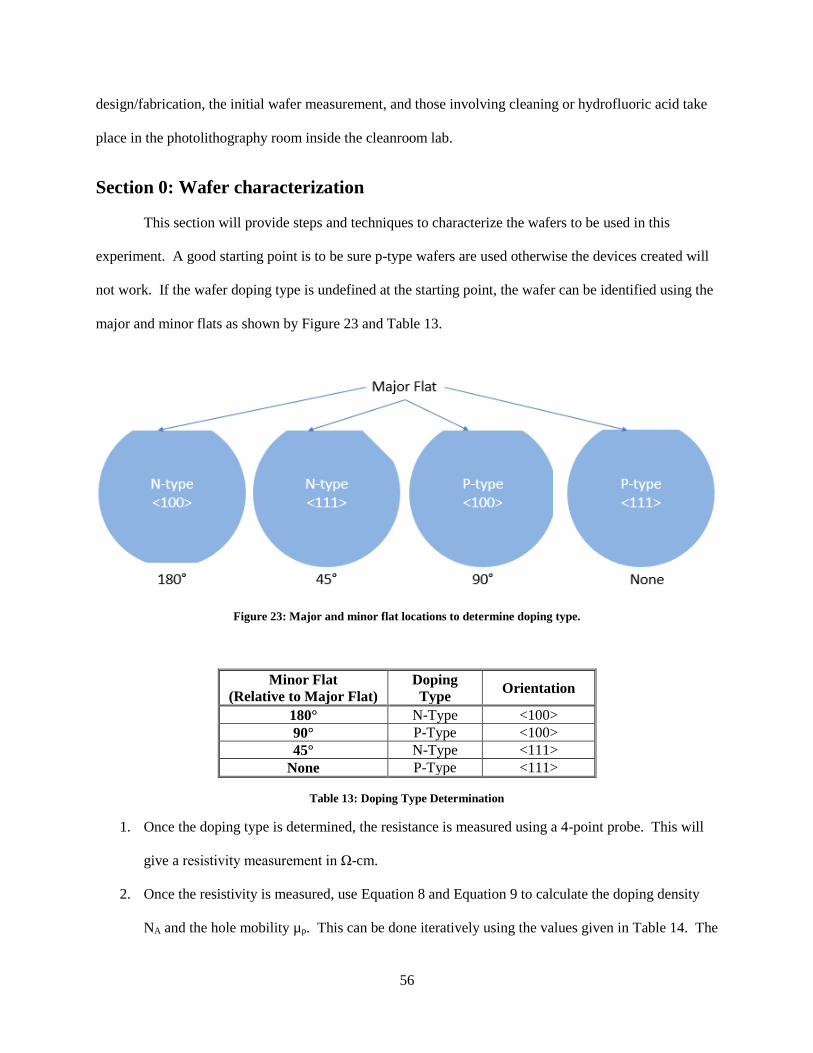
56
design/fabrication, the initial wafer measurement, and those involving cleaning or hydrofluoric acid take
place in the photolithography room inside the cleanroom lab.
Section 0: Wafer characterization
This section will provide steps and techniques to characterize the wafers to be used in this
experiment. A good starting point is to be sure p-type wafers are used otherwise the devices created will
not work. If the wafer doping type is undefined at the starting point, the wafer can be identified using the
major and minor flats as shown by Figure 23 and Table 13.
Figure 23: Major and minor flat locations to determine doping type.
Minor Flat
(Relative to Major Flat)
Doping
Type Orientation
180° N-Type <100>
90° P-Type <100>
45° N-Type <111>
None P-Type <111>
Table 13: Doping Type Determination
1. Once the doping type is determined, the resistance is measured using a 4-point probe. This will
give a resistivity measurement in Ω-cm.
2. Once the resistivity is measured, use Equation 8 and Equation 9 to calculate the doping density
NA and the hole mobility µp. This can be done iteratively using the values given in Table 14. The

57
recommended way to solve these equations is to create a column in Excel with doping densities
from 1*1014 and 5*1019 /cm3 in steps of 1000. In the column next to it, use Equation 8 to
calculated the hole mobility for each doping density. In a third column, use Equation 9 to
calculate the resistivity using the doping density and hole mobility calculated in the same row.
Once this is completed, the measured resistivity can be compared to the calculated resistivity and
the corresponding doping density and hole mobility can be determined.
Equation 8: The carrier mobility formula for non-intrinsic materials based on the doping concentration (N*) and fit
parameters including the reference doping concentration (Nref), the minimum mobility (µmin), and the low field carrier
mobility (µ0) the values for which are all available in Table 14 .
𝜇𝑝 = 𝜇𝑚𝑖𝑛 +𝜇0
1 + (𝑁𝐴
𝑁𝑟𝑒𝑓)
𝛼
Equation 9: The resistivity formula used to calculate the doping density of the devices.
𝜌 =1
𝑞(𝑁𝐴𝜇𝑝)
Symbol Name Value
q Electron charge (magnitude) 1.612*10-19 coul
k Boltzmann’s constant 8.617*10-5 eV/K
m0 Electron rest mass 9.11*10-31 kg
Nref Reference doping density Electrons: 1.3*1017 cm-3
Holes: 2.35*1017 cm-3
µmin Minimum carrier mobility
(fit parameter)
Electrons: 92 cm2/V-sec
Holes: 54.3 cm2/V-sec
µ0 Low Field electron or hole
mobility (fit parameter)
Electrons: 1268 cm2/V-sec
Holes: 406.9 cm2/V-sec
α Material Exponent
(fit parameter)
Electrons: 0.91
Holes: 0.88
NA Hole Doping Density Variable
ρ resistivity Variable, dependent on doping
density, units of Ω-cm
Table 14: Commonly used constants and symbols.
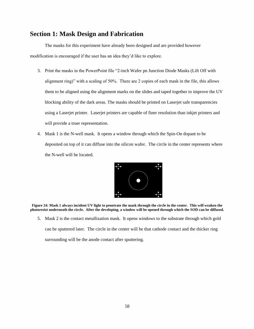
58
Section 1: Mask Design and Fabrication
The masks for this experiment have already been designed and are provided however
modification is encouraged if the user has an idea they’d like to explore.
3. Print the masks in the PowerPoint file “2-inch Wafer pn Junction Diode Masks (Lift Off with
alignment ring)” with a scaling of 50%. There are 2 copies of each mask in the file, this allows
them to be aligned using the alignment marks on the slides and taped together to improve the UV
blocking ability of the dark areas. The masks should be printed on Laserjet safe transparencies
using a Laserjet printer. Laserjet printers are capable of finer resolution than inkjet printers and
will provide a truer representation.
4. Mask 1 is the N-well mask. It opens a window through which the Spin-On dopant to be
deposited on top of it can diffuse into the silicon wafer. The circle in the center represents where
the N-well will be located.
Figure 24: Mask 1 always incident UV light to penetrate the mask through the circle in the center. This will weaken the
photoresist underneath the circle. After the developing, a window will be opened through which the SOD can be diffused.
5. Mask 2 is the contact metallization mask. It opens windows to the substrate through which gold
can be sputtered later. The circle in the center will be that cathode contact and the thicker ring
surrounding will be the anode contact after sputtering.
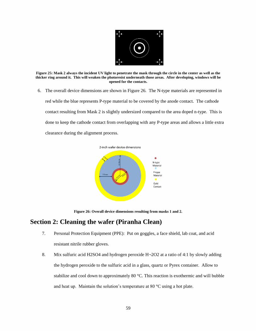
59
Figure 25: Mask 2 always the incident UV light to penetrate the mask through the circle in the center as well as the
thicker ring around it. This will weaken the photoresist underneath those areas. After developing, windows will be
opened for the contacts.
6. The overall device dimensions are shown in Figure 26. The N-type materials are represented in
red while the blue represents P-type material to be covered by the anode contact. The cathode
contact resulting from Mask 2 is slightly undersized compared to the area doped n-type. This is
done to keep the cathode contact from overlapping with any P-type areas and allows a little extra
clearance during the alignment process.
Figure 26: Overall device dimensions resulting from masks 1 and 2.
Section 2: Cleaning the wafer (Piranha Clean)
7. Personal Protection Equipment (PPE): Put on goggles, a face shield, lab coat, and acid
resistant nitrile rubber gloves.
8. Mix sulfuric acid H2SO4 and hydrogen peroxide H¬2O2 at a ratio of 4:1 by slowly adding
the hydrogen peroxide to the sulfuric acid in a glass, quartz or Pyrex container. Allow to
stabilize and cool down to approximately 80 °C. This reaction is exothermic and will bubble
and heat up. Maintain the solution’s temperature at 80 °C using a hot plate.

60
9. Using Anti-Acid Stainless Steel or Teflon tweezers, slowly place the 2-inch, p-type wafer
into the solution. If the wafer is submerged too quickly, it may crack. Leave the wafer
submerged in the solution for 15 minutes.
10. Remove the wafer from the solution using tweezers and rinse thoroughly using deionized
(DI) water. Repeat this rinse 3 times. DO NOT TOUCH THE WAFER WITH ANYTHING
OTHER THAN TWEEZERS! Any cleaning you had done up until this point would have to
be redone.
11. Blow dry using a Nitrogen gun and place in clean substrate holder or aluminum foil.
12. Measure 100 ml of de-ionized water and pour it into an HF safe developing tray (similar to
the tray shown in Figure 27). HDPE is a good material for the tray since it is HF safe.
13. Measure 10 ml of hydrofluoric acid (HF) in a HDPE graduated cylinder then add it to the
water in the developing tray. At no time should the acid come in contact with any part of the
protective equipment. If the HF is spilled, contact the lab manager who will take the
appropriate steps for cleanup. It is considered a good safety precaution to keep a 2.5%
calcium gluconate gel on hand in case the HF comes in contact with skin. Following a
through washing of the affected area using soap and water, the gel is applied to the skin to
neutralize the acid and stop the burning.
14. Stir the solution using Teflon tweezers and insert the 2-inch p-type silicon wafer. Gently
agitate the wafer to allow for all surfaces to be treated by the HF.
15. Remove the wafer from the solution using Teflon tweezers and rinse it in de-ionized water.
A steady stream of DI water is the preferred method to avoid contamination. If a steady DI
water stream is unavailable fill a HPDE beaker with 100 ml of DI water, submerge the wafer
in it and agitate slowly. Empty the water, refill, and repeat the rinse procedure twice more.
16. Remove the wafer from the water and dry it using a nitrogen gun. Once the wafer is dry,
place it in aluminum foil or on a cleanroom wipe.
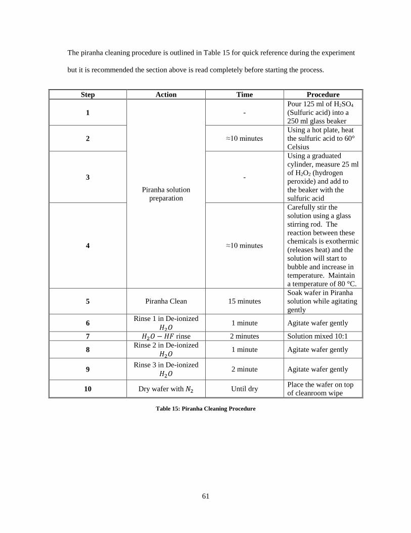
61
The piranha cleaning procedure is outlined in Table 15 for quick reference during the experiment
but it is recommended the section above is read completely before starting the process.
Step Action Time Procedure
1
Piranha solution
preparation
-
Pour 125 ml of H2SO4
(Sulfuric acid) into a
250 ml glass beaker
2 ≈10 minutes
Using a hot plate, heat
the sulfuric acid to 60°
Celsius
3 -
Using a graduated
cylinder, measure 25 ml
of H2O2 (hydrogen
peroxide) and add to
the beaker with the
sulfuric acid
4 ≈10 minutes
Carefully stir the
solution using a glass
stirring rod. The
reaction between these
chemicals is exothermic
(releases heat) and the
solution will start to
bubble and increase in
temperature. Maintain
a temperature of 80 °C.
5 Piranha Clean 15 minutes
Soak wafer in Piranha
solution while agitating
gently
6 Rinse 1 in De-ionized
𝐻2𝑂 1 minute Agitate wafer gently
7 𝐻2𝑂 − 𝐻𝐹 rinse 2 minutes Solution mixed 10:1
8 Rinse 2 in De-ionized
𝐻2𝑂 1 minute Agitate wafer gently
9 Rinse 3 in De-ionized
𝐻2𝑂 2 minute Agitate wafer gently
10 Dry wafer with 𝑁2 Until dry Place the wafer on top
of cleanroom wipe
Table 15: Piranha Cleaning Procedure
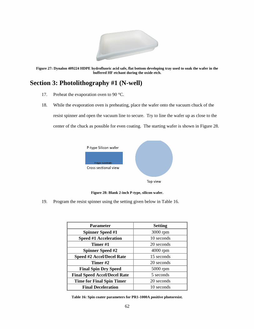
62
Figure 27: Dynalon 409224 HDPE hydrofluoric acid safe, flat bottom developing tray used to soak the wafer in the
buffered HF etchant during the oxide etch.
Section 3: Photolithography #1 (N-well)
17. Preheat the evaporation oven to 90 °C.
18. While the evaporation oven is preheating, place the wafer onto the vacuum chuck of the
resist spinner and open the vacuum line to secure. Try to line the wafer up as close to the
center of the chuck as possible for even coating. The starting wafer is shown in Figure 28.
Figure 28: Blank 2-inch P-type, silicon wafer.
19. Program the resist spinner using the setting given below in Table 16.
Parameter Setting
Spinner Speed #1 3000 rpm
Speed #1 Acceleration 10 seconds
Timer #1 20 seconds
Spinner Speed #2 4000 rpm
Speed #2 Accel/Decel Rate 15 seconds
Timer #2 20 seconds
Final Spin Dry Speed 5000 rpm
Final Speed Accel/Decel Rate 5 seconds
Time for Final Spin Timer 20 seconds
Final Deceleration 10 seconds
Table 16: Spin coater parameters for PR1-1000A positive photoresist.
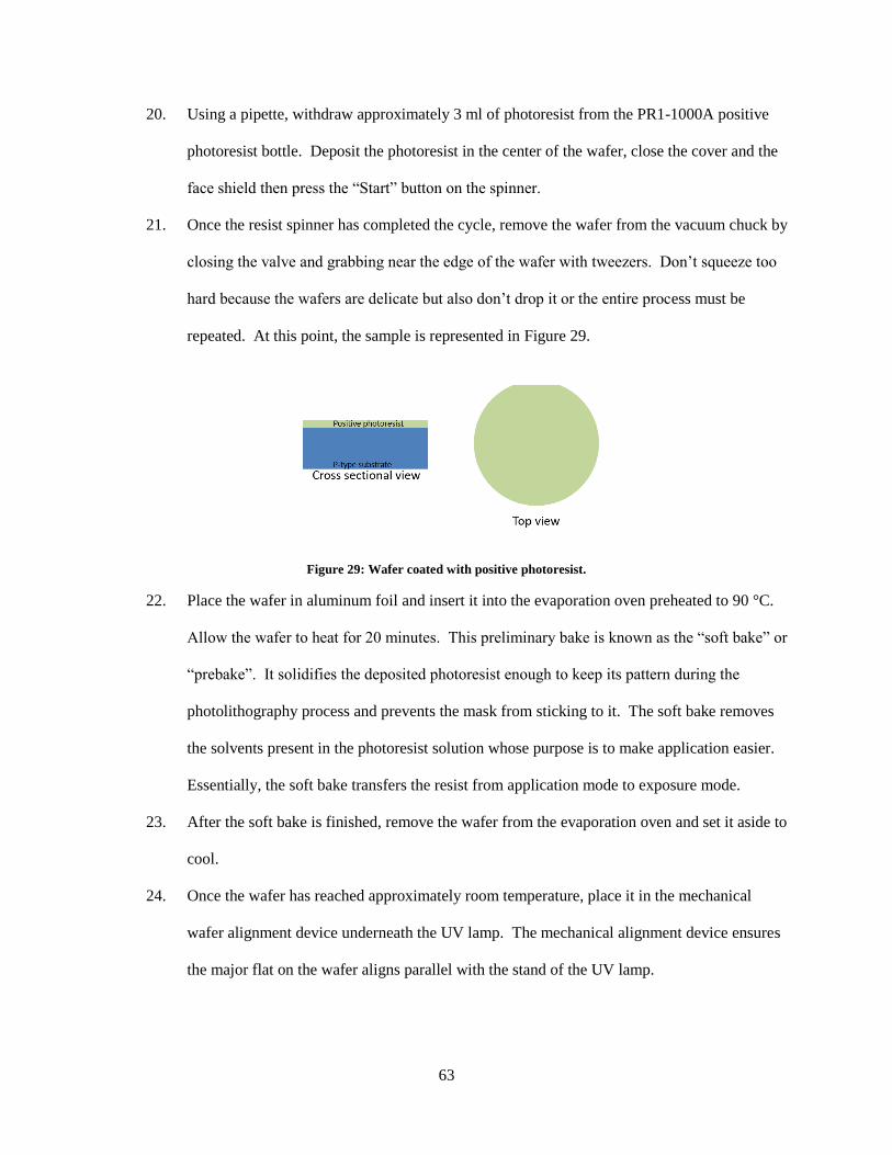
63
20. Using a pipette, withdraw approximately 3 ml of photoresist from the PR1-1000A positive
photoresist bottle. Deposit the photoresist in the center of the wafer, close the cover and the
face shield then press the “Start” button on the spinner.
21. Once the resist spinner has completed the cycle, remove the wafer from the vacuum chuck by
closing the valve and grabbing near the edge of the wafer with tweezers. Don’t squeeze too
hard because the wafers are delicate but also don’t drop it or the entire process must be
repeated. At this point, the sample is represented in Figure 29.
Figure 29: Wafer coated with positive photoresist.
22. Place the wafer in aluminum foil and insert it into the evaporation oven preheated to 90 °C.
Allow the wafer to heat for 20 minutes. This preliminary bake is known as the “soft bake” or
“prebake”. It solidifies the deposited photoresist enough to keep its pattern during the
photolithography process and prevents the mask from sticking to it. The soft bake removes
the solvents present in the photoresist solution whose purpose is to make application easier.
Essentially, the soft bake transfers the resist from application mode to exposure mode.
23. After the soft bake is finished, remove the wafer from the evaporation oven and set it aside to
cool.
24. Once the wafer has reached approximately room temperature, place it in the mechanical
wafer alignment device underneath the UV lamp. The mechanical alignment device ensures
the major flat on the wafer aligns parallel with the stand of the UV lamp.
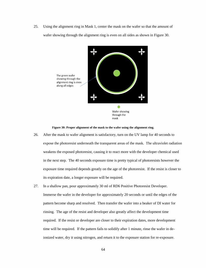
64
25. Using the alignment ring in Mask 1, center the mask on the wafer so that the amount of
wafer showing through the alignment ring is even on all sides as shown in Figure 30.
Figure 30: Proper alignment of the mask to the wafer using the alignment ring.
26. After the mask to wafer alignment is satisfactory, turn on the UV lamp for 40 seconds to
expose the photoresist underneath the transparent areas of the mask. The ultraviolet radiation
weakens the exposed photoresist, causing it to react more with the developer chemical used
in the next step. The 40 seconds exposure time is pretty typical of photoresists however the
exposure time required depends greatly on the age of the photoresist. If the resist is closer to
its expiration date, a longer exposure will be required.
27. In a shallow pan, pour approximately 30 ml of RD6 Positive Photoresist Developer.
Immerse the wafer in the developer for approximately 20 seconds or until the edges of the
pattern become sharp and resolved. Then transfer the wafer into a beaker of DI water for
rinsing. The age of the resist and developer also greatly affect the development time
required. If the resist or developer are closer to their expiration dates, more development
time will be required. If the pattern fails to solidify after 1 minute, rinse the wafer in de-
ionized water, dry it using nitrogen, and return it to the exposure station for re-exposure.
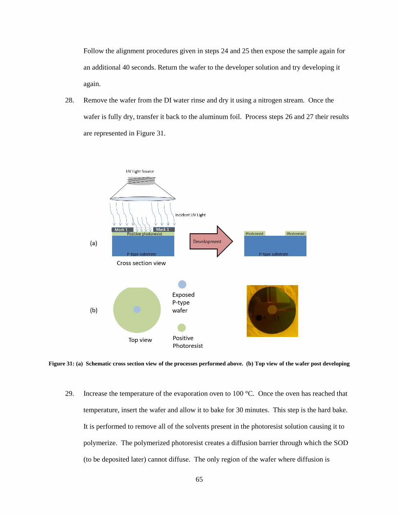
65
Follow the alignment procedures given in steps 24 and 25 then expose the sample again for
an additional 40 seconds. Return the wafer to the developer solution and try developing it
again.
28. Remove the wafer from the DI water rinse and dry it using a nitrogen stream. Once the
wafer is fully dry, transfer it back to the aluminum foil. Process steps 26 and 27 their results
are represented in Figure 31.
Figure 31: (a) Schematic cross section view of the processes performed above. (b) Top view of the wafer post developing
29. Increase the temperature of the evaporation oven to 100 °C. Once the oven has reached that
temperature, insert the wafer and allow it to bake for 30 minutes. This step is the hard bake.
It is performed to remove all of the solvents present in the photoresist solution causing it to
polymerize. The polymerized photoresist creates a diffusion barrier through which the SOD
(to be deposited later) cannot diffuse. The only region of the wafer where diffusion is
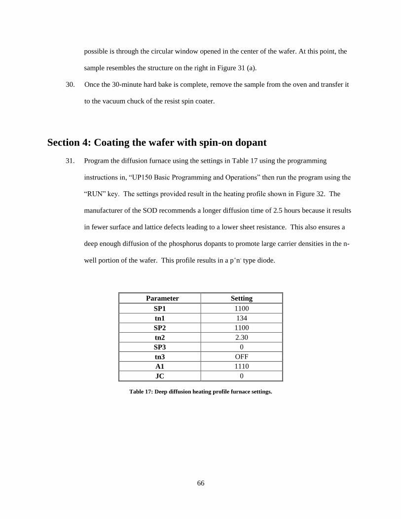
66
possible is through the circular window opened in the center of the wafer. At this point, the
sample resembles the structure on the right in Figure 31 (a).
30. Once the 30-minute hard bake is complete, remove the sample from the oven and transfer it
to the vacuum chuck of the resist spin coater.
Section 4: Coating the wafer with spin-on dopant
31. Program the diffusion furnace using the settings in Table 17 using the programming
instructions in, “UP150 Basic Programming and Operations” then run the program using the
“RUN” key. The settings provided result in the heating profile shown in Figure 32. The
manufacturer of the SOD recommends a longer diffusion time of 2.5 hours because it results
in fewer surface and lattice defects leading to a lower sheet resistance. This also ensures a
deep enough diffusion of the phosphorus dopants to promote large carrier densities in the n-
well portion of the wafer. This profile results in a p+n- type diode.
Parameter Setting
SP1 1100
tn1 134
SP2 1100
tn2 2.30
SP3 0
tn3 OFF
A1 1110
JC 0
Table 17: Deep diffusion heating profile furnace settings.
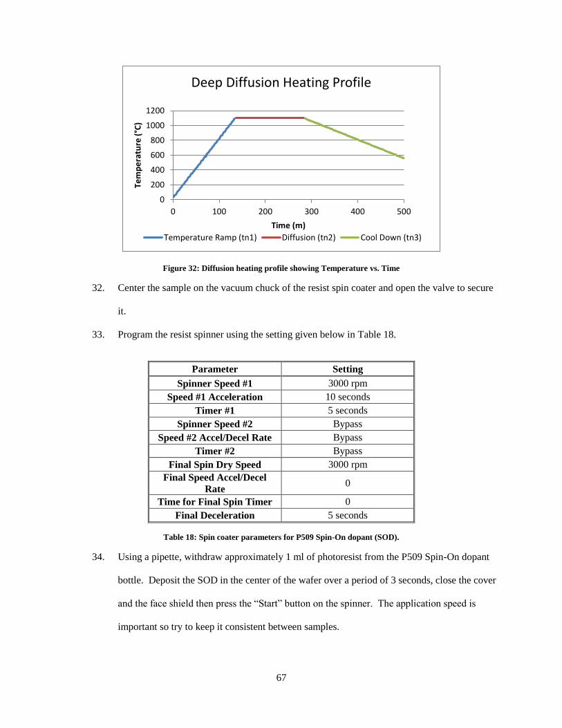
67
Figure 32: Diffusion heating profile showing Temperature vs. Time
32. Center the sample on the vacuum chuck of the resist spin coater and open the valve to secure
it.
33. Program the resist spinner using the setting given below in Table 18.
Parameter Setting
Spinner Speed #1 3000 rpm
Speed #1 Acceleration 10 seconds
Timer #1 5 seconds
Spinner Speed #2 Bypass
Speed #2 Accel/Decel Rate Bypass
Timer #2 Bypass
Final Spin Dry Speed 3000 rpm
Final Speed Accel/Decel
Rate 0
Time for Final Spin Timer 0
Final Deceleration 5 seconds
Table 18: Spin coater parameters for P509 Spin-On dopant (SOD).
34. Using a pipette, withdraw approximately 1 ml of photoresist from the P509 Spin-On dopant
bottle. Deposit the SOD in the center of the wafer over a period of 3 seconds, close the cover
and the face shield then press the “Start” button on the spinner. The application speed is
important so try to keep it consistent between samples.
0
200
400
600
800
1000
1200
0 100 200 300 400 500
Tem
pe
ratu
re (
°C)
Time (m)
Deep Diffusion Heating Profile
Temperature Ramp (tn1) Diffusion (tn2) Cool Down (tn3)
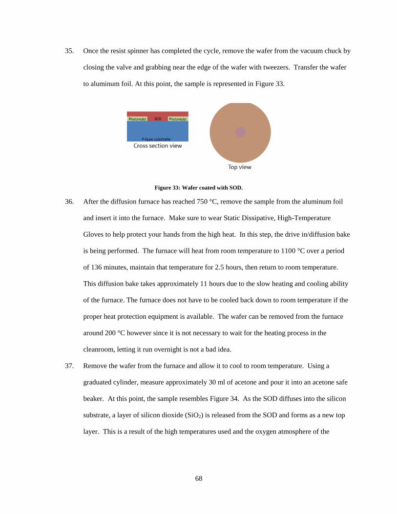
68
35. Once the resist spinner has completed the cycle, remove the wafer from the vacuum chuck by
closing the valve and grabbing near the edge of the wafer with tweezers. Transfer the wafer
to aluminum foil. At this point, the sample is represented in Figure 33.
Figure 33: Wafer coated with SOD.
36. After the diffusion furnace has reached 750 °C, remove the sample from the aluminum foil
and insert it into the furnace. Make sure to wear Static Dissipative, High-Temperature
Gloves to help protect your hands from the high heat. In this step, the drive in/diffusion bake
is being performed. The furnace will heat from room temperature to 1100 °C over a period
of 136 minutes, maintain that temperature for 2.5 hours, then return to room temperature.
This diffusion bake takes approximately 11 hours due to the slow heating and cooling ability
of the furnace. The furnace does not have to be cooled back down to room temperature if the
proper heat protection equipment is available. The wafer can be removed from the furnace
around 200 °C however since it is not necessary to wait for the heating process in the
cleanroom, letting it run overnight is not a bad idea.
37. Remove the wafer from the furnace and allow it to cool to room temperature. Using a
graduated cylinder, measure approximately 30 ml of acetone and pour it into an acetone safe
beaker. At this point, the sample resembles Figure 34. As the SOD diffuses into the silicon
substrate, a layer of silicon dioxide (SiO2) is released from the SOD and forms as a new top
layer. This is a result of the high temperatures used and the oxygen atmosphere of the
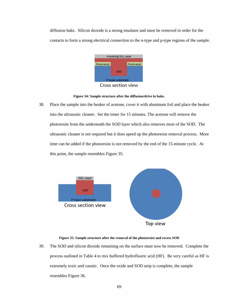
69
diffusion bake. Silicon dioxide is a strong insulator and must be removed in order for the
contacts to form a strong electrical connection to the n-type and p-type regions of the sample.
Figure 34: Sample structure after the diffusion/drive in bake.
38. Place the sample into the beaker of acetone, cover it with aluminum foil and place the beaker
into the ultrasonic cleaner. Set the timer for 15 minutes. The acetone will remove the
photoresist from the underneath the SOD layer which also removes most of the SOD. The
ultrasonic cleaner is not required but it does speed up the photoresist removal process. More
time can be added if the photoresist is not removed by the end of the 15-minute cycle. At
this point, the sample resembles Figure 35.
Figure 35: Sample structure after the removal of the photoresist and excess SOD
39. The SOD and silicon dioxide remaining on the surface must now be removed. Complete the
process outlined in Table 4 to mix buffered hydrofluoric acid (HF). Be very careful as HF is
extremely toxic and caustic. Once the oxide and SOD strip is complete, the sample
resembles Figure 36.
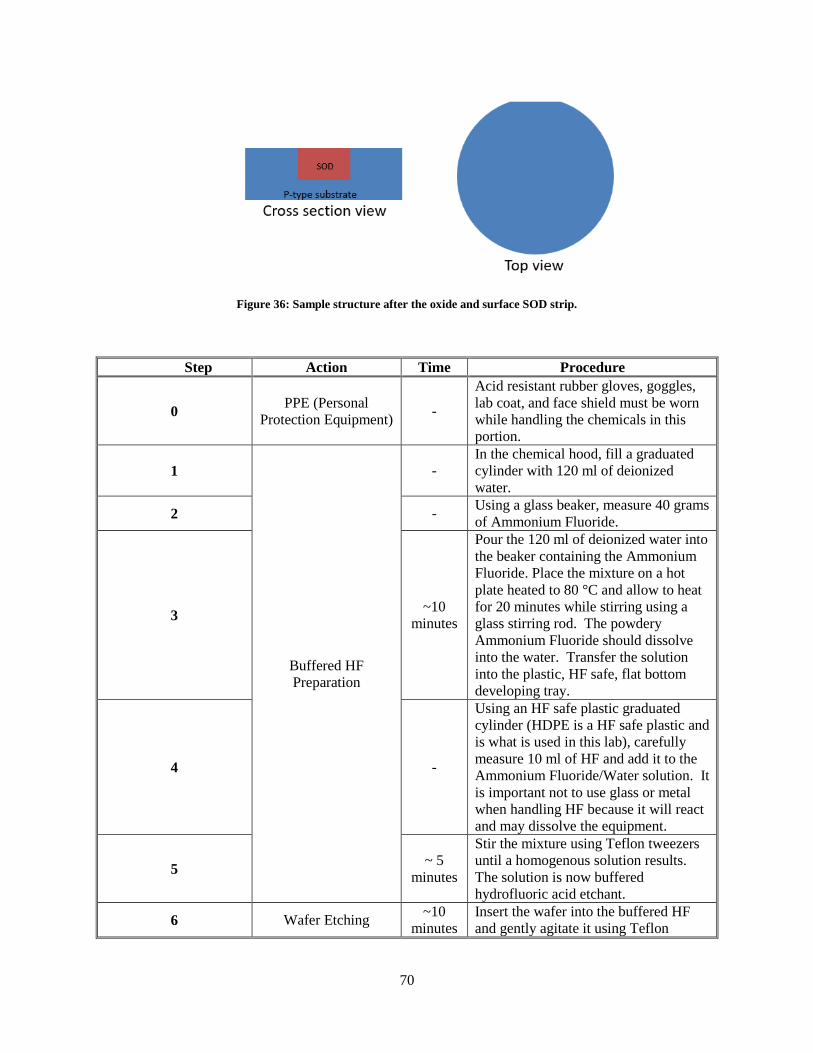
70
Figure 36: Sample structure after the oxide and surface SOD strip.
Step Action Time Procedure
0 PPE (Personal
Protection Equipment) -
Acid resistant rubber gloves, goggles,
lab coat, and face shield must be worn
while handling the chemicals in this
portion.
1
Buffered HF
Preparation
-
In the chemical hood, fill a graduated
cylinder with 120 ml of deionized
water.
2 - Using a glass beaker, measure 40 grams
of Ammonium Fluoride.
3 ~10
minutes
Pour the 120 ml of deionized water into
the beaker containing the Ammonium
Fluoride. Place the mixture on a hot
plate heated to 80 °C and allow to heat
for 20 minutes while stirring using a
glass stirring rod. The powdery
Ammonium Fluoride should dissolve
into the water. Transfer the solution
into the plastic, HF safe, flat bottom
developing tray.
4 -
Using an HF safe plastic graduated
cylinder (HDPE is a HF safe plastic and
is what is used in this lab), carefully
measure 10 ml of HF and add it to the
Ammonium Fluoride/Water solution. It
is important not to use glass or metal
when handling HF because it will react
and may dissolve the equipment.
5 ~ 5
minutes
Stir the mixture using Teflon tweezers
until a homogenous solution results.
The solution is now buffered
hydrofluoric acid etchant.
6 Wafer Etching ~10
minutes
Insert the wafer into the buffered HF
and gently agitate it using Teflon
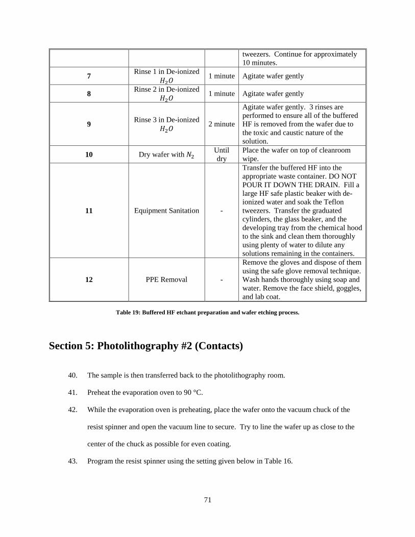
71
tweezers. Continue for approximately
10 minutes.
7 Rinse 1 in De-ionized
𝐻2𝑂 1 minute Agitate wafer gently
8 Rinse 2 in De-ionized
𝐻2𝑂 1 minute Agitate wafer gently
9 Rinse 3 in De-ionized
𝐻2𝑂 2 minute
Agitate wafer gently. 3 rinses are
performed to ensure all of the buffered
HF is removed from the wafer due to
the toxic and caustic nature of the
solution.
10 Dry wafer with 𝑁2 Until
dry
Place the wafer on top of cleanroom
wipe.
11 Equipment Sanitation -
Transfer the buffered HF into the
appropriate waste container. DO NOT
POUR IT DOWN THE DRAIN. Fill a
large HF safe plastic beaker with de-
ionized water and soak the Teflon
tweezers. Transfer the graduated
cylinders, the glass beaker, and the
developing tray from the chemical hood
to the sink and clean them thoroughly
using plenty of water to dilute any
solutions remaining in the containers.
12 PPE Removal -
Remove the gloves and dispose of them
using the safe glove removal technique.
Wash hands thoroughly using soap and
water. Remove the face shield, goggles,
and lab coat.
Table 19: Buffered HF etchant preparation and wafer etching process.
Section 5: Photolithography #2 (Contacts)
40. The sample is then transferred back to the photolithography room.
41. Preheat the evaporation oven to 90 °C.
42. While the evaporation oven is preheating, place the wafer onto the vacuum chuck of the
resist spinner and open the vacuum line to secure. Try to line the wafer up as close to the
center of the chuck as possible for even coating.
43. Program the resist spinner using the setting given below in Table 16.

72
44. Once the resist spinner has completed the cycle, remove the wafer from the vacuum chuck
by closing the valve and grabbing near the edge of the wafer with tweezers. At this point,
the sample is represented in Figure 37.
Figure 37: Sample structure after the second photoresist application.
45. Place the wafer in aluminum foil and insert it into the evaporation oven preheated to 90 °C.
Allow the wafer to heat for 20 minutes. This step is the soft bake for photolithography layer
2.
46. After the soft bake is finished, remove the wafer from the evaporation oven and set it aside to
cool.
47. Once the wafer has reached approximately room temperature, place it back into the
mechanical wafer alignment device underneath the UV lamp.
48. Using the alignment ring in Mask 2, center the mask on the wafer so that the amount of
wafer showing through the alignment ring is even as shown in Figure 38.

73
Figure 38: Proper alignment of the mask to the wafer using the alignment ring.
49. After the mask to wafer alignment is satisfactory, turn on the UV lamp for 40 seconds to
expose the photoresist underneath the transparent areas of the mask.
50. In a shallow pan, pour approximately 30 ml of RD6 Positive Photoresist Developer.
Immerse the wafer in the developer for approximately 20 seconds or until the edges of the
pattern become sharp and resolved. Then transfer the wafer into a beaker of DI water for
rinsing. As with the previous developing, if the features fail to appear with sharp features,
rinse the sample, dry it with nitrogen, repeat the alignment procedure, re-expose it, and
repeat the developing process.
51. Remove the wafer from the DI water rinse and dry it using a nitrogen stream. Once the
wafer is fully dry, transfer it back to the aluminum foil. At this point, the sample is
represented by Figure 39.
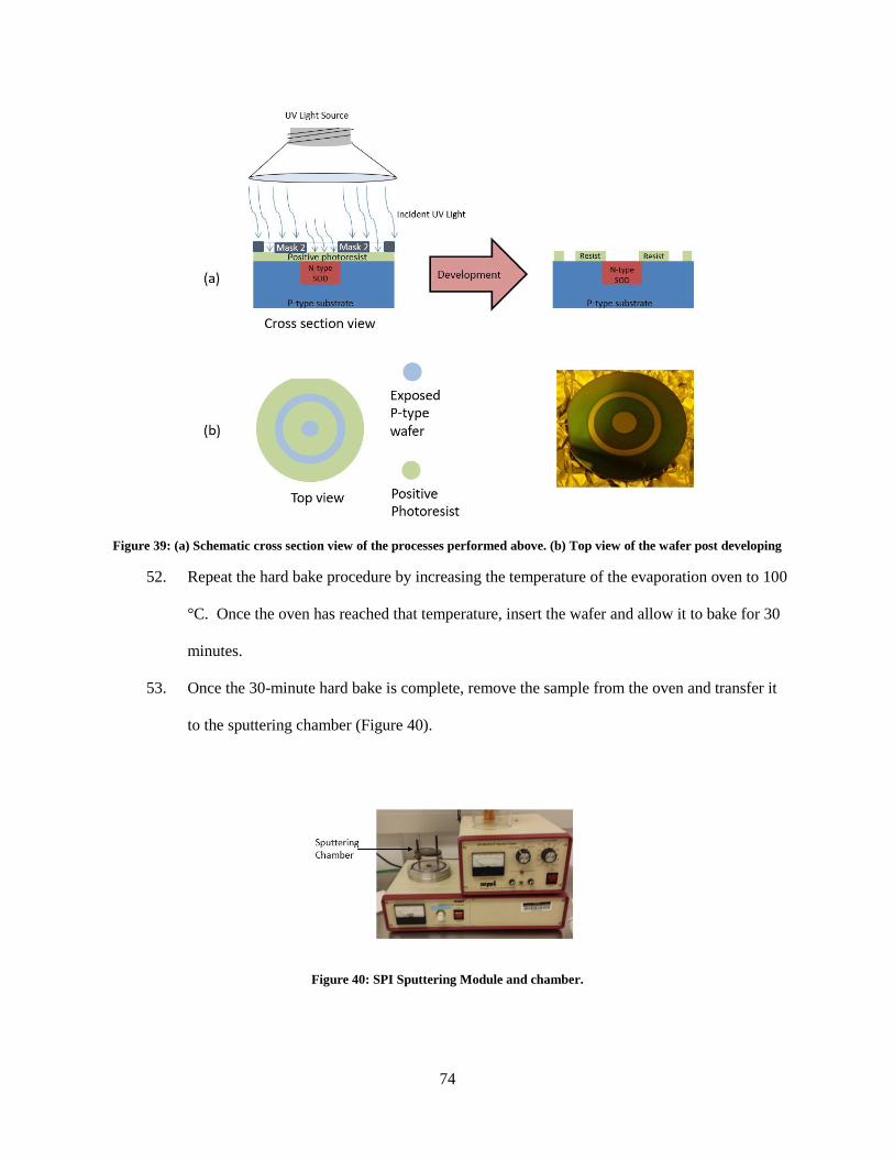
74
Figure 39: (a) Schematic cross section view of the processes performed above. (b) Top view of the wafer post developing
52. Repeat the hard bake procedure by increasing the temperature of the evaporation oven to 100
°C. Once the oven has reached that temperature, insert the wafer and allow it to bake for 30
minutes.
53. Once the 30-minute hard bake is complete, remove the sample from the oven and transfer it
to the sputtering chamber (Figure 40).
Figure 40: SPI Sputtering Module and chamber.
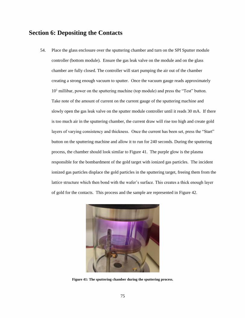
75
Section 6: Depositing the Contacts
54. Place the glass enclosure over the sputtering chamber and turn on the SPI Sputter module
controller (bottom module). Ensure the gas leak valve on the module and on the glass
chamber are fully closed. The controller will start pumping the air out of the chamber
creating a strong enough vacuum to sputter. Once the vacuum gauge reads approximately
101 millibar, power on the sputtering machine (top module) and press the “Test” button.
Take note of the amount of current on the current gauge of the sputtering machine and
slowly open the gas leak valve on the sputter module controller until it reads 30 mA. If there
is too much air in the sputtering chamber, the current draw will rise too high and create gold
layers of varying consistency and thickness. Once the current has been set, press the “Start”
button on the sputtering machine and allow it to run for 240 seconds. During the sputtering
process, the chamber should look similar to Figure 41. The purple glow is the plasma
responsible for the bombardment of the gold target with ionized gas particles. The incident
ionized gas particles displace the gold particles in the sputtering target, freeing them from the
lattice structure which then bond with the wafer’s surface. This creates a thick enough layer
of gold for the contacts. This process and the sample are represented in Figure 42.
Figure 41: The sputtering chamber during the sputtering process.
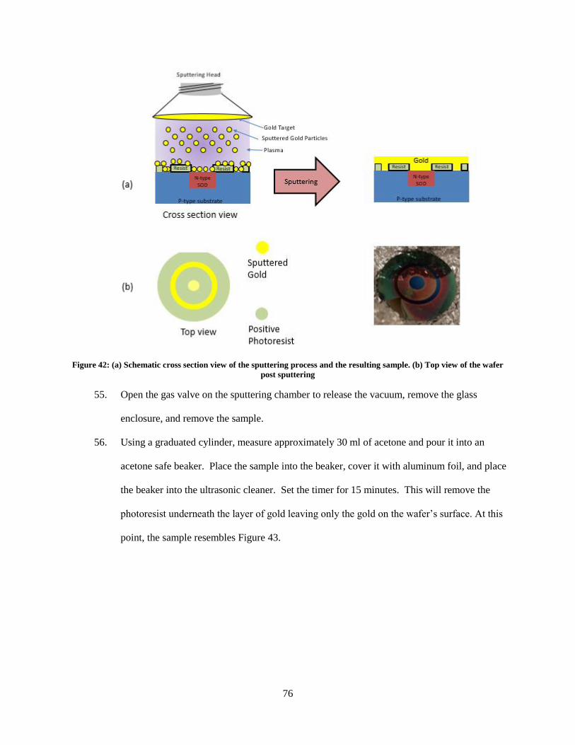
76
Figure 42: (a) Schematic cross section view of the sputtering process and the resulting sample. (b) Top view of the wafer
post sputtering
55. Open the gas valve on the sputtering chamber to release the vacuum, remove the glass
enclosure, and remove the sample.
56. Using a graduated cylinder, measure approximately 30 ml of acetone and pour it into an
acetone safe beaker. Place the sample into the beaker, cover it with aluminum foil, and place
the beaker into the ultrasonic cleaner. Set the timer for 15 minutes. This will remove the
photoresist underneath the layer of gold leaving only the gold on the wafer’s surface. At this
point, the sample resembles Figure 43.
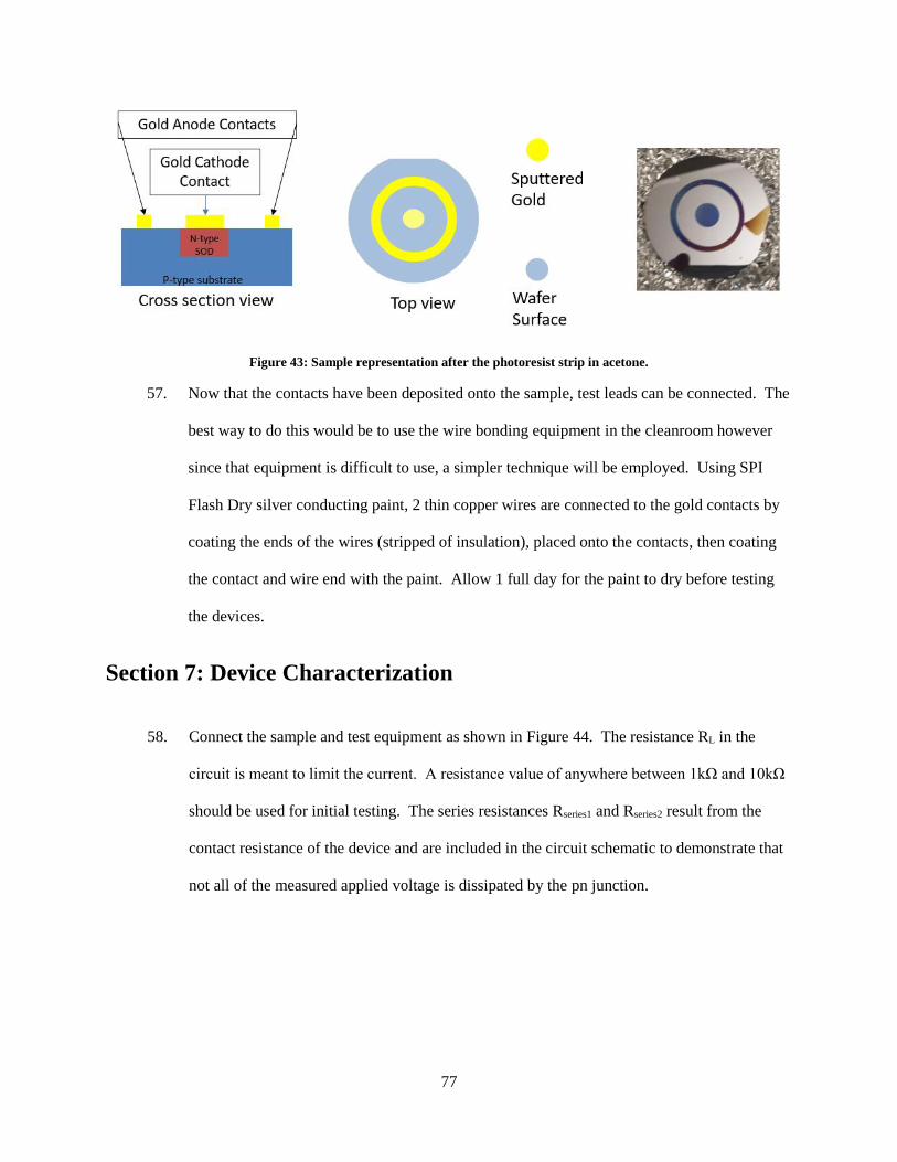
77
Figure 43: Sample representation after the photoresist strip in acetone.
57. Now that the contacts have been deposited onto the sample, test leads can be connected. The
best way to do this would be to use the wire bonding equipment in the cleanroom however
since that equipment is difficult to use, a simpler technique will be employed. Using SPI
Flash Dry silver conducting paint, 2 thin copper wires are connected to the gold contacts by
coating the ends of the wires (stripped of insulation), placed onto the contacts, then coating
the contact and wire end with the paint. Allow 1 full day for the paint to dry before testing
the devices.
Section 7: Device Characterization
58. Connect the sample and test equipment as shown in Figure 44. The resistance RL in the
circuit is meant to limit the current. A resistance value of anywhere between 1kΩ and 10kΩ
should be used for initial testing. The series resistances Rseries1 and Rseries2 result from the
contact resistance of the device and are included in the circuit schematic to demonstrate that
not all of the measured applied voltage is dissipated by the pn junction.
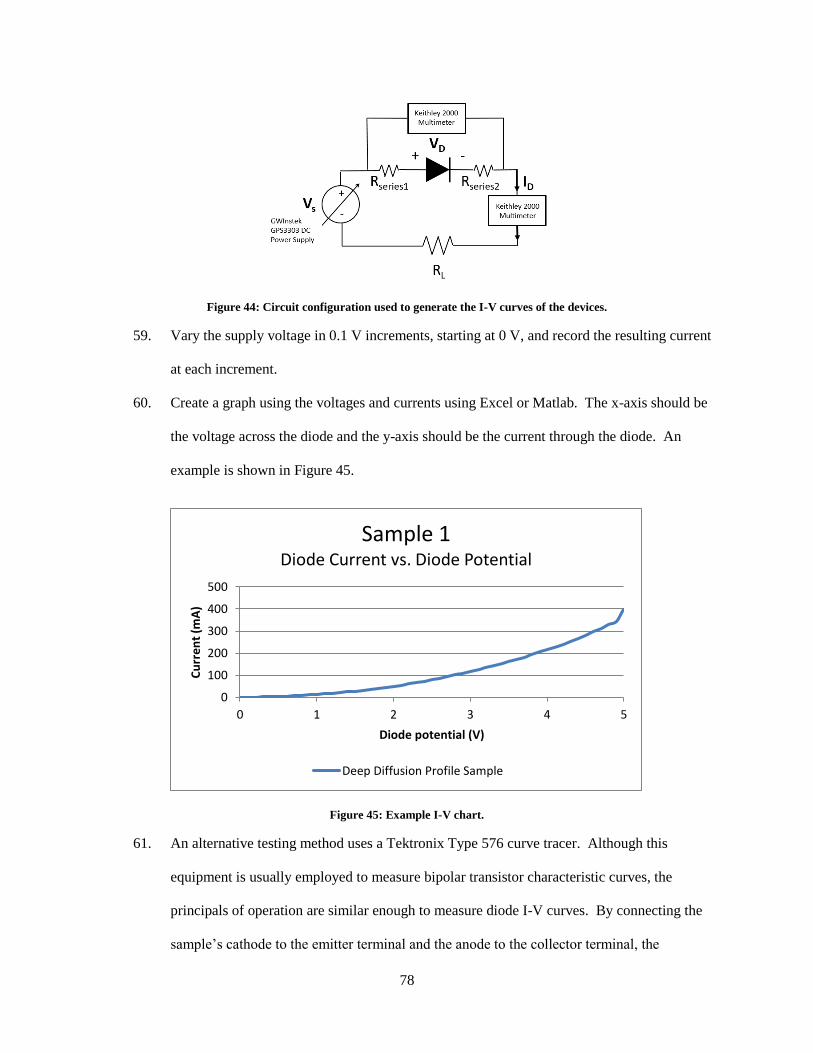
78
Figure 44: Circuit configuration used to generate the I-V curves of the devices.
59. Vary the supply voltage in 0.1 V increments, starting at 0 V, and record the resulting current
at each increment.
60. Create a graph using the voltages and currents using Excel or Matlab. The x-axis should be
the voltage across the diode and the y-axis should be the current through the diode. An
example is shown in Figure 45.
Figure 45: Example I-V chart.
61. An alternative testing method uses a Tektronix Type 576 curve tracer. Although this
equipment is usually employed to measure bipolar transistor characteristic curves, the
principals of operation are similar enough to measure diode I-V curves. By connecting the
sample’s cathode to the emitter terminal and the anode to the collector terminal, the
0
100
200
300
400
500
0 1 2 3 4 5
Cu
rre
nt
(mA
)
Diode potential (V)
Sample 1Diode Current vs. Diode Potential
Deep Diffusion Profile Sample
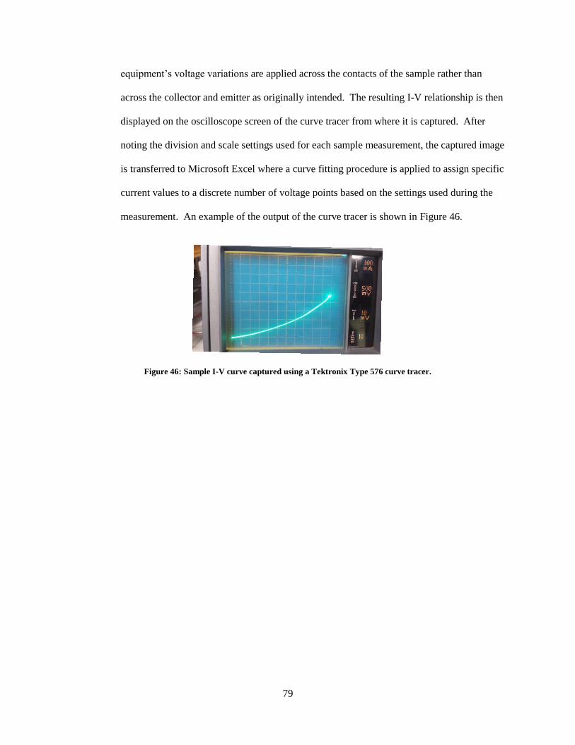
79
equipment’s voltage variations are applied across the contacts of the sample rather than
across the collector and emitter as originally intended. The resulting I-V relationship is then
displayed on the oscilloscope screen of the curve tracer from where it is captured. After
noting the division and scale settings used for each sample measurement, the captured image
is transferred to Microsoft Excel where a curve fitting procedure is applied to assign specific
current values to a discrete number of voltage points based on the settings used during the
measurement. An example of the output of the curve tracer is shown in Figure 46.
Figure 46: Sample I-V curve captured using a Tektronix Type 576 curve tracer.

80
Bibliography
aBeam Technologies, Inc. (2016). Clean Job Specification/Pricing. Retrieved from aBeam Technologies:
http://www.abeamtech.com/?dir=products/Photomasks&pg=Pricing
Ali, K., Khan, S. A., & Jafri, Z. M. (2012). Spin-On Doping (SOD) and Diffusion Temperature Effect on
Re-Combinations/Ideality Factor for Solar Cell Applications. Chalcogenide Letters, 457-563.
Artwork Conversion Software, Inc. (n.d.). L-Edit Plot and L-Edit DXF Pricing. Retrieved from
www.artwork.com: http://www.artwork.com/tanner/price.htm
Brigham Young University, Department of Electrical & Computer Engineering. (2016). Resistivity &
Mobility Calculator/Graph for Various Doping Concentrations in Silicon. Retrieved from
Cleanroom.byu.edu: http://www.cleanroom.byu.edu/ResistivityCal.phtml
Fair, R. R., & Tsai, I. C. (1977). A Quantitative Model for the Diffusion of Phosphorus in Silicon and the
Emitter Dip Effect. Chemisher Inofrmationdienst, 1107-1113. doi:10.1149/1.2133492
Filmtronics Inc. (2004). Spin-On Diffusants. Butler, PA: Filmtronics Inc.
Gangopadhyay, U., Kim, K., Dhungel, S. K., & Yi, J. (2005). Effect of novel surface treatment on large-
area low-cost SOD diffused monocrystalline silicon solar cells. Journal of the Korean Physical
Society, 47(6), 1035-1040.
Gopalan, C., Chakraborty, P. S., Yang, J., Kim, T., Wu, Z., McCartney, M. R., . . . Throton, T. J. (2003,
May). Shallow Source/Drain Extensions for Deep Submicron MOSFETs Using Spin-on-Dopants.
IEEE Transactions on Electron Devices, 50(5), 1277-1283.
Hamammu, I., & Ibrahim, K. (2003). Low Cost Fabrication For High Efficiency Monocyrstalline Silcon
Solar Cells. 3rd World Conference on Photovoltaic Energy Conversion. 2, pp. 1519-1520. Osaka,
Japan: Late News Paper.
Honsberg, C., & Boden, S. (n.d.). Surface Texturing. Retrieved October 16, 2016, from PVEducation.org:
http://www.pveducation.org/pvcdrom/design/surface-texturing
Morsin, M. b., Zulkipli, A. M., Sulong, M. S., & Rahman, T. b. (2009). Mask Design, Fabrication and
Characterization Of In-House N-Well MOSFET Using Spin-On Dopant Technique for
Undergraduates Program. IEEE Symposium on Industrial Electronics and Applications, 485-489.
Naseem, H. A., & Brown, W. D. (1999). Integrated circuit fabrication technology and laboratory courses
at the University of Arkansas. University/Government/Industry Microelectronics Symposium,
1999. Proceedings of the Thirteenth Biennial. IEEE. doi:10.1109/UGIM.1999.782811
Neudeck, G. W., & Luginbuhl, H. W. (1970, November 12). Laboratory Experiments in the Fabrication
of Thick-Film and Thin-Film Integrated Circuits. IEEE Transactions on Education, E-13(4), 192-
195. doi:10.1109/TE.1970.4320624
81
Neudeck, G. W., Luginbuhl, H. W., & Silva, L. F. (1970, August). An Undergraduate Integrated Circuit
Fabrication Laboratory. IEEE Transactions on Education, 13(2), 73-77.
doi:10.1109/TE.1970.4320567
Pierret, R. F. (1996). Semiconductor Device Fundamentals. Reading, MA: Addison-Wesley Publishing
Company. doi:0-20t-54393-l
Poole, I. (n.d.). Understanding diode specifications & parameters- a summary of the diode specifications
and diode parameters and ratings seen in datasheets with explanations of what they mean.
Retrieved 12 9, 2014, from Radio-Electronics.com: http://www.radio-
electronics.com/info/data/semicond/diodes/specifications-parameters-ratings-characteristics.php
Solecon Labratories, Inc. (n.d.). Solecon Labs Technical Note: Doping Type Determination. Reno, NV.
Szmyd, D. M. (1995). An Undergraduate Laboratory in the Design, Fabrication and Test of
Semiconductor Processes. University/Government/Industry Microelectronics Symposium, 1995.,
Proceedings of the Eleventh Biennial (pp. 31-35). IEEE. doi:10.1109/UGIM.1995.514112
Teh, S. T., & Chuah, D. S. (1989, December 27). Diffusion Profile of Spin-On Dopant in Silicon
Substrate. Solar Energy Materials, 19(3-5), 237-247.
Yokogawa M&C Corporation. (2001). Model UP150 Program Temperature Controller. User's Manual.
Retrieved from
http://mfc.engr.arizona.edu/documents/Oxidation%20Furnace/UP150%20Programming%20Man
ual.pdf
Zant, P. V. (2004). Microchip fabrication: a practical guide to semiconductor processing. fifth edition.
Retrieved from http://common.books24x7.com/toc.aspx?bookid=15225
82
Curriculum Vitae
Richard Robert Ryan
Phone: (702)-781-0110
Email address: [email protected] or [email protected]
Degrees:
Bachelor of Science, Electrical Engineering, 2012
University of Nevada, Las Vegas
Thesis Title: Process Development for the Fabrication of Semiconductor Devices and Circuits Using
Spin-On Dopant
Thesis Examination Committee:
Chairperson, Dr. Biswajit Das
Committee Member, Dr. Yahia Baghzouz
Committee Member, Dr. Yingtao Jiang
Graduate Faculty Representative, Dr. Frank van Breukelen