MOSFET Metal-Oxide Semiconductor Field-Effect...
23
EE2002 1 MOSFET Metal-Oxide Semiconductor Field-Effect Transistor EE2002 Analog Electronics
Transcript of MOSFET Metal-Oxide Semiconductor Field-Effect...
EE2002 1
MOSFETMetal-Oxide Semiconductor Field-Effect
Transistor
EE2002 Analog Electronics
EE2002 2
Scope
• Operation of MOSFET• Characteristics in operation regions of cutoff, triode and
saturation.• Symbols to represent MOSFET in circuit schematics.• Circuits for biasing transistors into different operating
regions.
• READ CHAPTER 4 J&B TEXTBOOK
EE2002 3
Types of Field-Effect Transistors
• MOSFET (Metal-Oxide Semiconductor Field-Effect Transistor)– Primary component in high-density VLSI chips Two
types of MOSFET: enhancement and depletion• ONLY enhancement MOSFET included in this course
EE2002 4
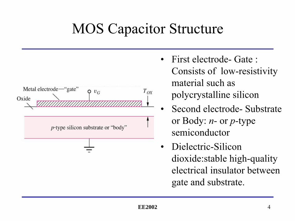
MOS Capacitor Structure
• First electrode- Gate : Consists of low-resistivitymaterial such as polycrystalline silicon
• Second electrode- Substrate or Body: n- or p-type semiconductor
• Dielectric-Silicon dioxide:stable high-quality electrical insulator between gate and substrate.
EE2002 5
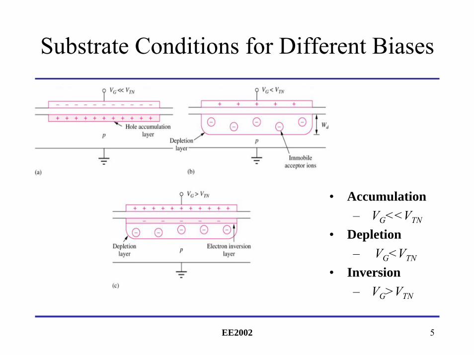
Substrate Conditions for Different Biases
• Accumulation – VG<<VTN
• Depletion– VG<VTN
• Inversion– VG>VTN
EE2002 6
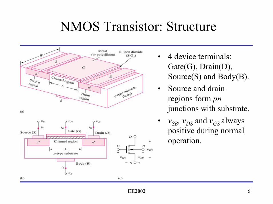
NMOS Transistor: Structure
• 4 device terminals: Gate(G), Drain(D), Source(S) and Body(B).
• Source and drain regions form pnjunctions with substrate.
• vSB, vDS and vGS always positive during normal operation.
EE2002 7
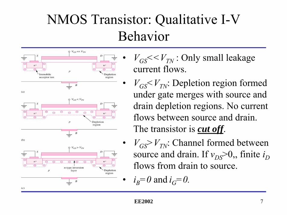
NMOS Transistor: Qualitative I-V Behavior• VGS<<VTN : Only small leakage
current flows.• VGS<VTN: Depletion region formed
under gate merges with source and drain depletion regions. No current flows between source and drain. The transistor is cut off.
• VGS>VTN: Channel formed between source and drain. If vDS>0,, finite iDflows from drain to source.
• iB=0 and iG=0.
EE2002 8
NMOS Transistor: Triode Region Characteristics
=Di
DSv2DSv
TNVGSvnKDi ⎟⎠
⎞⎜⎝
⎛−−=
Kn’=μnCox’’ (A/V2)
Cox’’=εox/Tox
μn= electron mobility (cm2/V.s)
εox= oxide permittivity (F/cm)
Tox=oxide thickness (cm)
for 0≥≥− DSvTNVGSv
where, Kn= Kn’W/L
EE2002 9
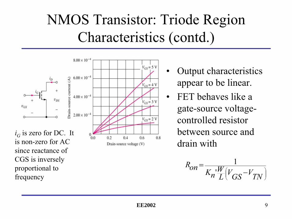
NMOS Transistor: Triode Region Characteristics (contd.)
• Output characteristics appear to be linear.
• FET behaves like a gate-source voltage-controlled resistor between source and drain with
⎟⎟⎠
⎞⎜⎜⎝
⎛ −=
TNVGSVLW
nKonR'
1
iG is zero for DC. It is non-zero for AC since reactance of CGS is inversely proportional to frequency
EE2002 10
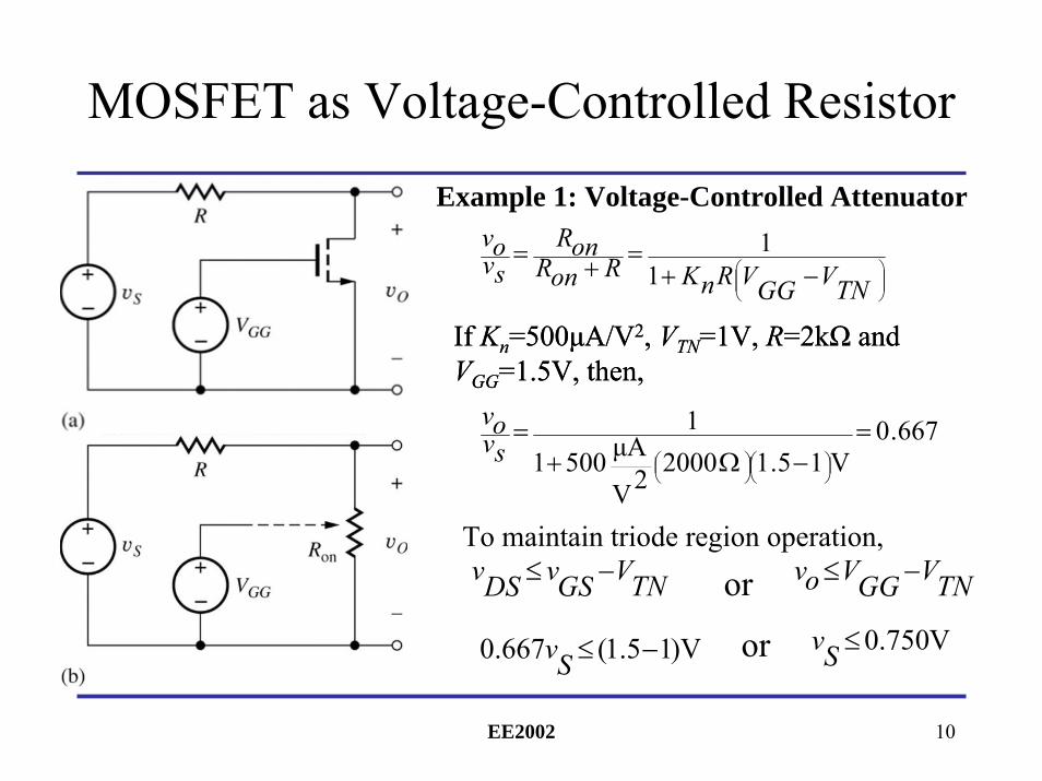
MOSFET as Voltage-Controlled Resistor
Example 1: Voltage-Controlled Attenuator
⎟⎟⎠
⎞⎜⎜⎝
⎛ −+=+=
TNVGGVRnKRonRonR
svov
11
If Kn=500μA/V2, VTN=1V, R=2kΩ and VGG=1.5V, then,
667.0V15.120002V
μA50011 =
−Ω+=
⎟⎠⎞⎜
⎝⎛⎟
⎠⎞⎜
⎝⎛sv
ov
To maintain triode region operation,
V)15.1(667.0 −≤Sv or V750.0≤Sv
TNVGGVov −≤orTNVGSvDSv −≤
If Kn=500μA/V2, VTN=1V, R=2kΩ and VGG=1.5V, then,
EE2002 11
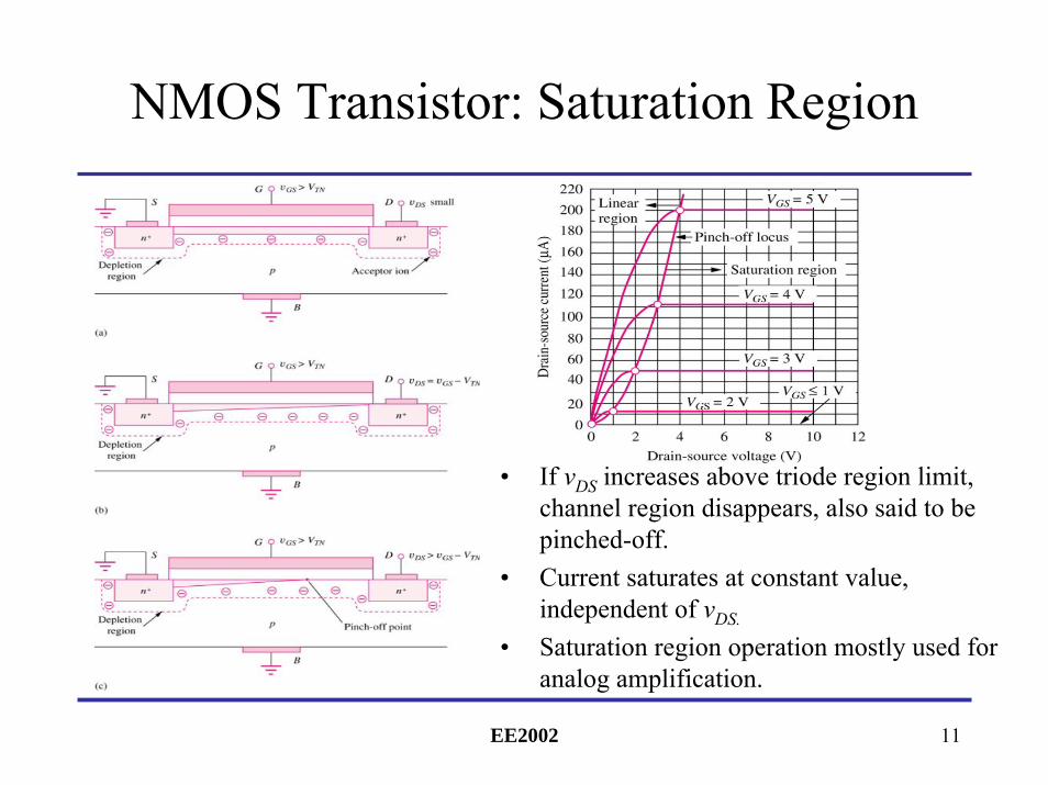
NMOS Transistor: Saturation Region
• If vDS increases above triode region limit, channel region disappears, also said to be pinched-off.
• Current saturates at constant value, independent of vDS.
• Saturation region operation mostly used for analog amplification.
EE2002 12
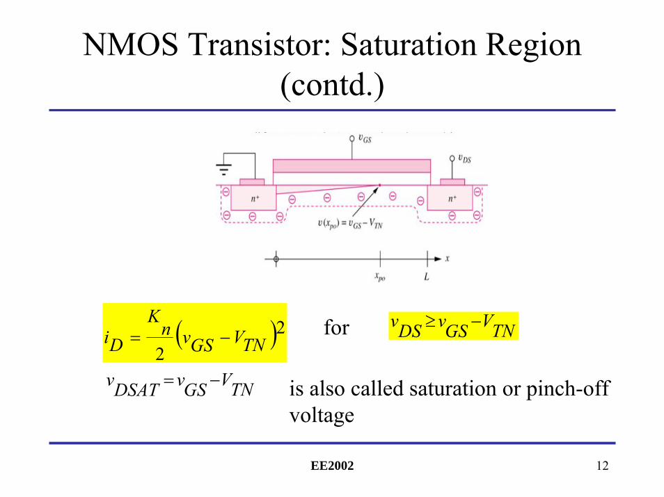
NMOS Transistor: Saturation Region (contd.)
( )22 TNVGSvn
KDi −= for TNVGSvDSv −≥
TNVGSvDSATv −= is also called saturation or pinch-off voltage
EE2002 13
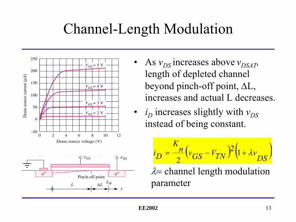
Channel-Length Modulation
• As vDS increases above vDSAT,length of depleted channel beyond pinch-off point, ΔL, increases and actual L decreases.
• iD increases slightly with vDSinstead of being constant.
( ) ( )DS
vTNVGSvnK
Di λ+−= 122
λ= channel length modulation parameter
EE2002 14
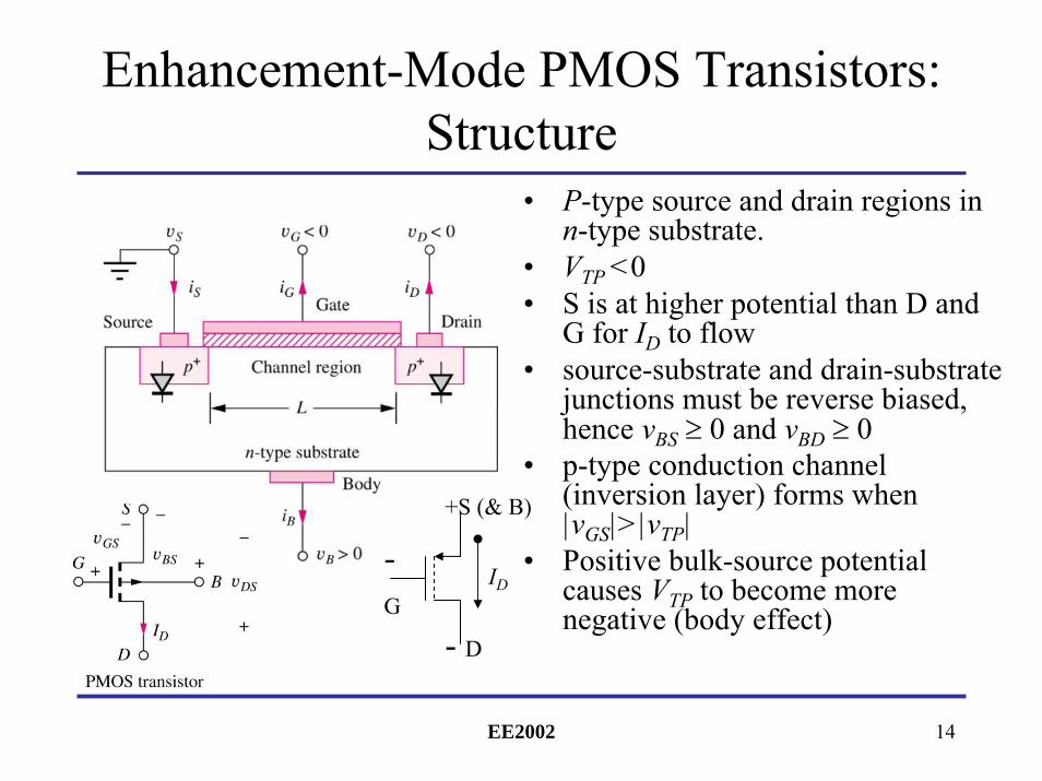
Enhancement-Mode PMOS Transistors: Structure
• P-type source and drain regions in n-type substrate.
• VTP <0• S is at higher potential than D and
G for ID to flow • source-substrate and drain-substrate
junctions must be reverse biased, hence vBS ≥ 0 and vBD ≥ 0
• p-type conduction channel (inversion layer) forms when |vGS|>|vTP|
• Positive bulk-source potential causes VTP to become more negative (body effect)
+S (& B)
- D
-G
ID
EE2002 15
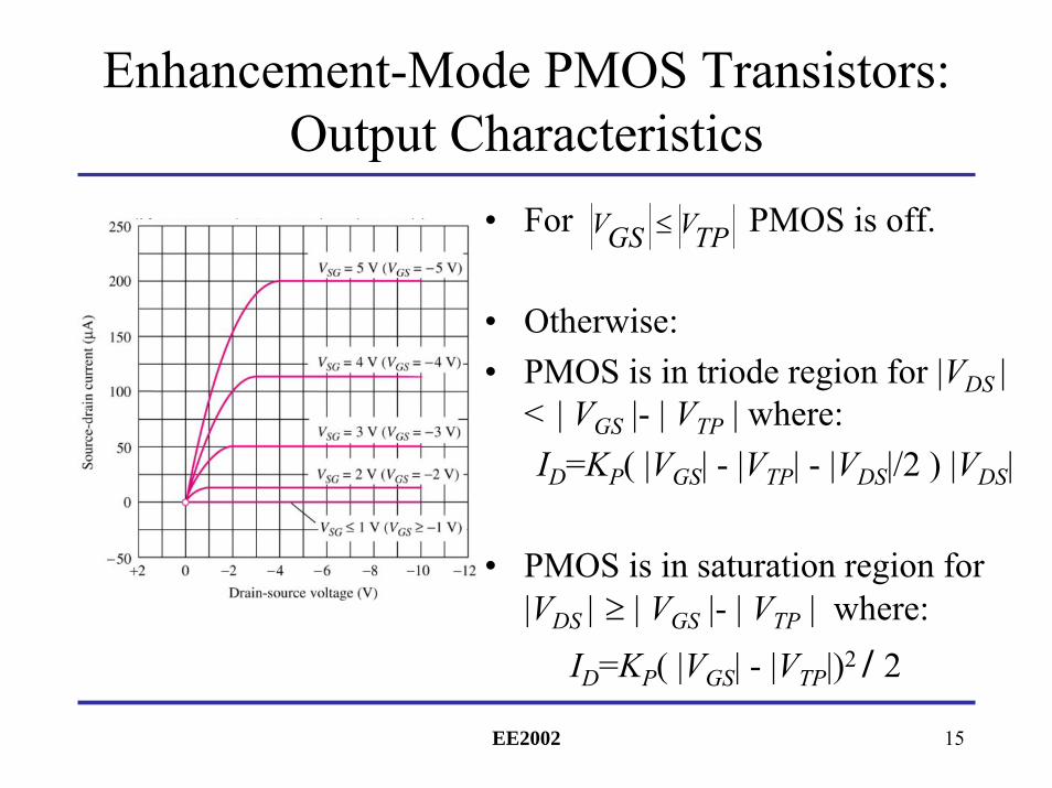
Enhancement-Mode PMOS Transistors: Output Characteristics
• For PMOS is off.
• Otherwise: • PMOS is in triode region for |VDS |
< | VGS |- | VTP | where:ID=KP( |VGS| - |VTP| - |VDS|/2 ) |VDS|
• PMOS is in saturation region for |VDS | ≥ | VGS |- | VTP | where:
ID=KP( |VGS| - |VTP|)2 / 2
TPVGSV ≤
EE2002 16
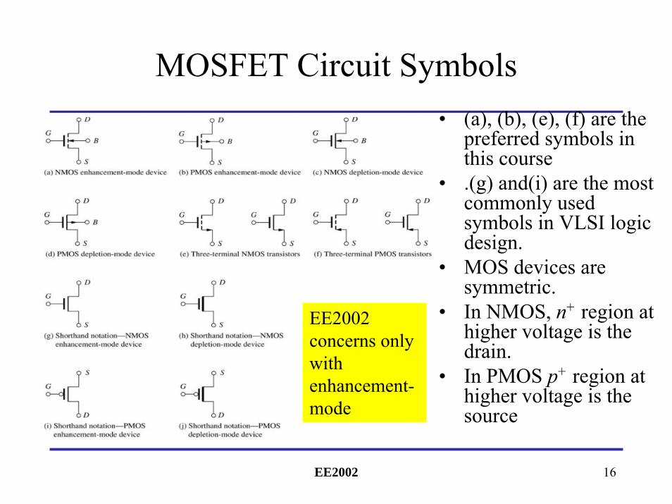
MOSFET Circuit Symbols• (a), (b), (e), (f) are the
preferred symbols in this course
• .(g) and(i) are the most commonly used symbols in VLSI logic design.
• MOS devices are symmetric.
• In NMOS, n+ region at higher voltage is the drain.
• In PMOS p+ region at higher voltage is the source
EE2002 concerns only with enhancement-mode
EE2002 17
Bias Analysis Approach
• Assume saturation region (unless operation region is obvious)
• Use circuit analysis to find VGS• Use VGS to calculate ID, and ID to find VDS• Check validity of operation region assumption• Change assumption and analyze again if required.
NOTE :An enhancement-mode device with VDS = VGS is always in saturation because |VDS | always greater than (|VGS|-|VTX|), where X is either N or P
EE2002 18
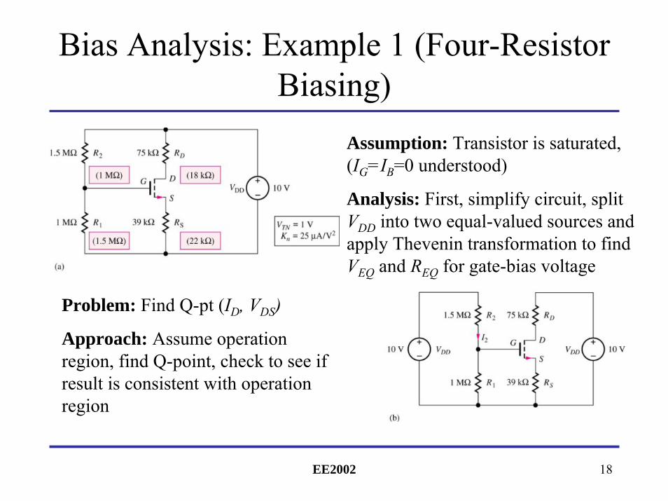
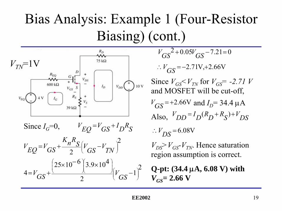
Bias Analysis: Example 1 (Four-Resistor Biasing)
Problem: Find Q-pt (ID, VDS)
Approach: Assume operation region, find Q-point, check to see if result is consistent with operation region
Assumption: Transistor is saturated, (IG=IB=0 understood)
Analysis: First, simplify circuit, split VDD into two equal-valued sources and apply Thevenin transformation to find VEQ and REQ for gate-bias voltage
EE2002 19
Bias Analysis: Example 1 (Four-Resistor Biasing) (cont.)
SRDIGSVEQV +=Since IG=0,
2
2 ⎟⎟⎠
⎞⎜⎜⎝
⎛ −+= TNVGSVSRnKGSVEQV
21
2
4109.3610254 ⎟⎟
⎠
⎞⎜⎜⎝
⎛⎟⎟⎠
⎞⎜⎜⎝
⎛⎟⎟⎠
⎞⎜⎜⎝
⎛
−×−×
+= GSVGSV
021.705.02 =−+ GSVGSV
V66.2,V71.2 +−=∴ GSV
Since VGS<VTN for VGS= -2.71 V and MOSFET will be cut-off,
V66.2+=GSV and ID= 34.4 μA
DSAlso, VSRDRDIDDV ++= )(
V08.6=∴ DSV
VDS>VGS-VTN. Hence saturation region assumption is correct.
Q-pt: (34.4 μA, 6.08 V) with VGS= 2.66 V
VTN=1V
EE2002 20
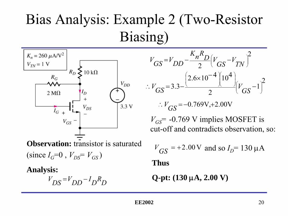
Bias Analysis: Example 2 (Two-Resistor Biasing)
Observation: transistor is saturated (since IG=0 , VDS= VGS )
Analysis:DRDIDDVDSV −=
2
2 ⎟⎟⎠
⎞⎜⎜⎝
⎛ −−= TNVGSVDRnKDDVGSV
21
2
4104106.23.3 ⎟⎟
⎠
⎞⎜⎜⎝
⎛⎟⎟⎠
⎞⎜⎜⎝
⎛⎟⎟⎠
⎞⎜⎜⎝
⎛
−
−×−=∴ GSVGSV
V00.2,V769.0 +−=∴ GSV
VGS= -0.769 V implies MOSFET is cut-off and contradicts observation, so:
V00.2+=GSV and so ID= 130 μA
Thus
Q-pt: (130 μA, 2.00 V)
EE2002 21
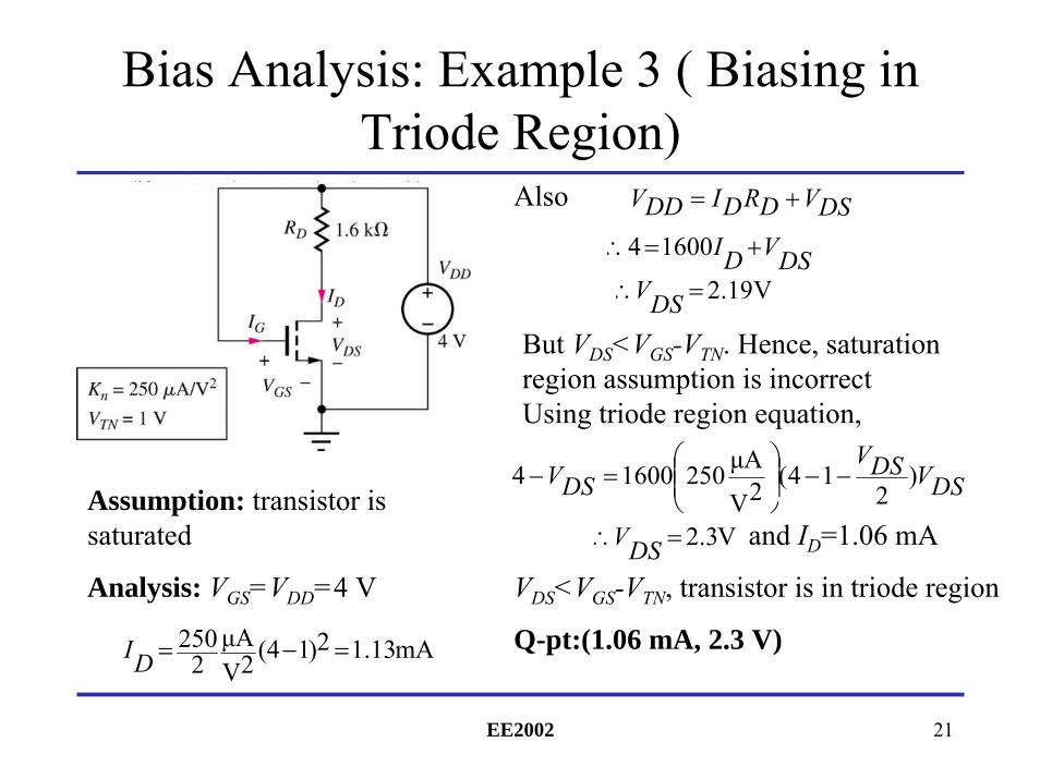
Bias Analysis: Example 3 ( Biasing in Triode Region)
Assumption: transistor is saturated
Analysis: VGS=VDD=4 V
mA13.12)14(2VμA
2250 =−=DI
DSVDRDIDDV +=Also
V19.2=∴ DSV
But VDS<VGS-VTN. Hence, saturation region assumption is incorrect Using triode region equation,
DSVDI +=∴ 16004
DSVDSVDSV )
214(2V
μA25016004 −−⎟⎟⎠
⎞⎜⎜⎝
⎛=−
V3.2=∴ DSV and ID=1.06 mA
VDS<VGS-VTN, transistor is in triode region
Q-pt:(1.06 mA, 2.3 V)
EE2002 22
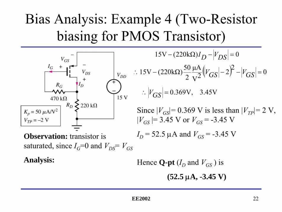
Bias Analysis: Example 4 (Two-Resistor biasing for PMOS Transistor)
Observation: transistor is saturated, since IG=0 and VDS= VGS
Analysis:
0)kΩ220(V15 =−− DSVDI
( ) 0222VμA
250)kΩ220(V15 =−−−∴ GSVGSV
V45.3,V369.0=∴ GSV
Since |VGS|= 0.369 V is less than |VTP|= 2 V, |VGS |= 3.45 V or VGS = -3.45 V
ID = 52.5 μA and VGS = -3.45 V
Hence Q-pt (ID and VGS ) is
(52.5 μA, -3.45 V)
EE2002 23
End Part 1