İSTANBUL TECHNICAL UNIVERSITY INSTITUTE OF … · MOSFET : Metal-Oxide-Semiconductor Field-Effect...
83
i İSTANBUL TECHNICAL UNIVERSITY INSTITUTE OF SCIENCE AND TECHNOLOGY M.Sc. Thesis by Alper KURDOGLU (504041003) Date of submission : 21 September 2007 Date of defence examination: 11 October 2007 Supervisor (Chairman): Asst. Prof. Dr. Özgür ÜSTÜN Members of the Examining Committee Prof.Dr. Oruç BİLGİÇ (Y.T.Ü.) Prof.Dr. Metin GÖKAŞAN (İ.T.Ü.) DECEMBER 2007 BRUSHLESS DC MOTOR SPEED CONTROL CIRCUIT DESIGN
Transcript of İSTANBUL TECHNICAL UNIVERSITY INSTITUTE OF … · MOSFET : Metal-Oxide-Semiconductor Field-Effect...
i
İSTANBUL TECHNICAL UNIVERSITY INSTITUTE OF SCIENCE AND TECHNOLOGY
M.Sc. Thesis by Alper KURDOGLU
(504041003)
Date of submission : 21 September 2007
Date of defence examination: 11 October 2007
Supervisor (Chairman): Asst. Prof. Dr. Özgür ÜSTÜN
Members of the Examining Committee Prof.Dr. Oruç BİLGİÇ (Y.T.Ü.)
Prof.Dr. Metin GÖKAŞAN (İ.T.Ü.)
DECEMBER 2007
BRUSHLESS DC MOTOR SPEED CONTROL CIRCUIT
DESIGN

ii
İSTANBUL TEKNİK ÜNİVERSİTESİ FEN BİLİMLERİ ENSTİTÜSÜ
BRUSHLESS DC MOTOR SPEED CONTROL CIRCUIT DESIGN
YÜKSEK LİSANS TEZİ Alper KURDOĞLU
(504041003)
ARALIK 2007
Tezin Enstitüye Verildiği Tarih : 21 Eylül 2007
Tezin Savunulduğu Tarih : 11 Ekim 2007
Tez Danışmanı : Yrd.Doç.Dr. Özgür ÜSTÜN
Diğer Jüri Üyeleri Prof.Dr. Oruç Bilgiç (Y.T.Ü.)
Prof.Dr. Metin GÖKAŞAN (İ.T.Ü.)

iii
PREFACE
This study has focused to Closed Loop Speed Control Application of a BLDC Motor.
I have tried to design a control circuit based upon MC33035 microcontroller
produced by the MOTOROLA and gave the theory of operation regarding the
application.
I am sincerely grateful to my instructor Asst. Prof. Dr. Özgür ÜSTÜN who made
many contributions to this Project. I have learned many things about the PCB design
and Power Electronics from him.
I would also like to thank my department manager MSc. Civil Engineer Ali Levent
Kuzum for his helps and sensibility in my difficult thesis process. His goodwill was
very motivating in my stressfull days.
My valuable thanks go to my family for their limitless tolerance. Their approach was
very helpful and valuable to me.
Lastly, I like to thank my friend Can Gökçe for introducing and providing me the
Altium Designer Software which was very useful in the process of designing the
PCB circuit.
SEPTEMBER 2007 ALPER KURDOĞLU

iv
CONTENTS
ABBREVIATIONS vi TABLE LIST vii FIGURE LIST viii SYMBOL LIST ix ÖZET xi SUMMARY xii
1. INTRODUCTION.................................................................................................. 1 1.1. Brushless DC Motor Drives .................................................................................. 1
2. BLDC MOTORS.................................................................................................... 3 2.1. General Characteristics ...................................................................................... 3 2.2. Construction .......................................................................................................... 4
2.2.1. Stator Structure .......................................................................................... 4
2.1.2. Rotor Structure........................................................................................... 5
2.1.3. Hall Sensors ............................................................................................... 6 2.3. Mathematical Model of Brushless DC Motor....................................................... 7 2.4. Torque Equation of Brushless DC Motor ........................................................... 17 2.5. Fundementals of BLDC Motor Operation .......................................................... 18
3. BLDC MOTOR CONTROL............................................................................... 19 3.1. Torque-Speed Quadrant Concept.................................................................... 19
3.1.1. One Quadrant Control .............................................................................. 19
3.1.2. Two Quadrants Control............................................................................ 20
3.1.3. Four Quadrants Control............................................................................ 21 3.2. Closed Loop Speed Control Theory................................................................ 22 3.3. Digital Control and Commutation................................................................... 23
4. CLOSED LOOP SPEED CONTROL DRIVER ............................................... 25 4.1. Driver Construction......................................................................................... 25
4.1.1. MC 33035 IC ........................................................................................... 25
4.1.1.1. Rotor Position Decoder 29
4.1.1.2. Error Amplifier 29
4.1.1.3. Oscillator 29
4.1.1.4. Pulse Width Modulator 30
4.1.2. MC33039 Electronic Tachometer 30
4.1.3. MSK3003 Power Module 31 4.2. Assembyling the Circuit 32
4.2.1. Timing Components 32

v
4.2.2. Drive Circuits 32
4.2.2.1. N-Channel Gate Drive Circuit 34
4.2.2.2. P-Channel Gate Drive Circuit 34 4.3. Control Features 35
4.3.1. Open Loop Speed Control 36
4.3.2. Closed Loop Speed Control 36 4.4. Commutation 38
4.4.1. Rotor Position Decoder 38
4.4.2. Commutation Process 38 4.5. Fault Management 45
4.5.1. Over Current Detection 45
4.5.1.1. Overcurrent Sensing 45
4.5.1.2. Current Limiting 46
4.5.2. Undervoltage Lockout 47
4.5.3. Thermal Shutdown 47 4.6. Braking 47
5. PRINTED CIRCUIT BOARD (PCB) DESIGN 48 5.1. Creating the PCB Project on Altium Designer 48 5.2. Creating and Drawing the Schematic Document-Circuit 48 5.3. Locating the Component and Loading the Libraries 48 5.4. Creating a New PCB Document and Component Layout 49 6. EXPERIMENTAL WORK 54 6.1. The Speed Control of the Motor 55 6.2. Speed Feedback 58
7. CONCLUSION 61
BIBLIOGRAPHY 63
RESUMEE 64
APPENDIX 65

vi
ABBREVIATIONS
BLDC : Brushless DC Motor EMF : Electromotor Force EPROM : Erasable Programmable read-only memory PWM : Pulse Wide Modulation PI : Proportional Integral PID : Proportional Integral Derivative MOSFET : Metal-Oxide-Semiconductor Field-Effect Transistor LED : Light-Emitting Diode AMP : Amplificator IC : Integrated Circuit PCB : Printed Circuit Board GND :Ground PWR :Power FWD :Forward REV :Reverse
vii
LIST OF TABLES
Page Number
Tablo 2.1 Commutation Intervals Depending on Rotor Position for One Electrical Rotation
7
Table 4.1 MC33035 Pin Descriptions 21 Table 4.2 Switching sequence and resulting air-gap field direction 33 Table 6.1 Speed Control Experiment Result 60

viii
FIGURE LIST Page Number
Figure 2.1 Figure 2.2 Figure 2.3 Figure 2.4 Figure 2.5 Figure 2.6 Figure 3.1 Figure 3.2 Figure 3.3 Figure 3.4 Figure 3.5 Figure 4.1 Figure 4.2 Figure 4.3 Figure 4.4 Figure 4.5 Figure 4.6 Figure 4.7 Figure 4.8 Figure 4.9 Figure 4.10 Figure 4.11 Figure 4.12 Figure 5.1 Figure 5.2 Figure 5.3 Figure 5.4 Figure 5.5 Figure 5.6 Figure 5.7 Figure 6.1 Figure 6.2 Figure 6.3 Figure 6.4 Figure 6.5 Figure 6.6 Figure 6.7 Figure 6.8 Figure 6.9 Figure 6.10 Figure 6.11
: Trapezoidal Back EMF............................................................... : Sinusoidal Back EMF................................................................. : Roto Magnet Cross Section........................................................ : BLDC Motor Transfer Section................................................. . : Conduction equivalent circuit for the invertal………………... : Conduction equivalent circuit for the invertal………………... : Single Quadrant DC Motor Drive Circuit.................................. : Six steps drive system for BLDC motor..................................... : Speed Controller.......................................................................... : Voltage Strokes Applied to the 3-Phase BLDC Motor................: 3-Phase BLDC Power Stage....................................................... : MC33035 Pin Connections........................................................ : MC33035 Representative Block Diagram.................................. : Error Amplifier........................................................................... : Pulse Width Modulator Timing Diagram................................... : MC33039 block diagram............................................................ : MSK3003 circuit scheme............................................................ :Timing Diagram of A Three Phase, Six Step Motor Application :Closed Loop Brushless DC Motor Control ………………… : The Functional Block Diagram of the System………………. : Principle Commutation Circuit of A Brushless D.C. motor. : Four-poles permanent magnet .................................................... : Three Phase, Six Step, Full Wave Commutation Waveforms ... : Schematic Form of the Closed Speed Control Circuit............... : The Best Layout Plan Discovered After Many Times of Trials. : The Best Layout Plan Output…………………………………. : PCB Format with the Layers Connections……………………. : Five jumping connections........................................................... : Final PCB ready for the manufacturing……………………….. : The Manufactured PCB.............................................................. : Voltage waveform in %50 PWM................................................ : Voltage waveform in %100 PWM............................................. : Current Waveform...................................................................... : The Brushless Motor loaded with a DC Generator.................... : The Improved Test Setup……………………………………… : The Close View of the Line Voltage at Low PWM…………... : The Close View of the line Voltage at High PWM …………... : The Frequency Ouput of the Motor Speed……………………. : Accelerating of motor from standstill to maximum speed…….. : The waveform of MC33039 output for slightly loaded motor… : The waveform of MC33039 output for slightly loaded motor
4 5 5 6 8 9
19 21 22 24 24 26 27 29 30 31 31 33 35
37 39 40 42 49 50 50 51 52 53 53 54 54 55 55 56 57 57 58 59 60 60

ix
SYMBOL LIST
k stepin error Input :)(ke
k stepin valueDesired:w(k)
k stepin valueMeasuredm(k) =
k stepin output Controller u(k) =
k stepin portion output alProportion(k)u p =
k stepin portion output Integral (k)u I =
1-k stepin portion output Integral 1)-(ku I =
constant timeIntegral TI =
timeSampling T =
gain Controller KC =
rotor on the induced Torque=indτ
Field MagneticRotor =RB
Field MagneticStator =SB
DC=DCBU
DCBU = DC bus voltage
=TC Timing capacitor
=TR Timing Resistor
=ai A phase current
=bi B phase current
=ci C phase current
=aR A phase stator winding resistance
=bR B phase stator winding resistance
=cR C phase stator winding resistance
=aL A phase stator winding inductance
=bL B phase stator winding inductance
=cL C phase stator winding inductance
=aE Induced voltage on the a phase stator winding

x
=bE Induced voltage on the b phase stator winding
=cE Induced voltage on the c phase stator winding
=ω Angular velocity M= Torqute
=mM Motor torque
=yM Load torque
=k Motor constant =ak Motor constant for A phase
=bk Motor constant for B phase
=ck Motor constant for C phase
=θ Rotor position angle =J Moment of Inertia

xi
FIRÇASIZ DOĞRU AKIM MOTORU HIZ KONTROL DEVRESİ TASARIMI
ÖZET
Günümüzde fırçasız doğru akım motorları gün geçtikçe önem kazanmakta ve
yaygınlaşmaktadır. Fırçalı doğru akım motorlarıyla karşılaştırıldığında fırçasız doğru
akım motorlarında komütasyon işlemi mekanik olarak fırçalarla değil elektronik
olarak yapılmaktadır ve bu kullanışlılıklarını arttırır. Fırçasız doğru akım
motorlarında rotorun manyetik yapısı tarafından üretilen manyetik alan motorun
verimliliğini arttırır bu yüzde fırçasız doğru akım motorlarının çok geniş bir kullanım
alanı vardır. Bu tez çalışması 3 fazlı bir fırçasız doğru akım motorunun kapalı çevrim
hız kontrolünü yapan bir sürücü devrenin yapılması ve devrenin çalışma ilkesinin
açıklanmasını hedef almıştır. Yakın zamana kadar fırçasız doğru akım motorlarının
avantajlarından yararlanmak isteyen motor üreticileri önemli bir sorunla
karşılaşmışlardır. Bu sorun Hall sensörlerden gelen digital sinyalleri çözümleyecek
ve bunun yanında bir motorun sorunsuz çalışması için gerekli bazı fonksiyonları
yerine getirecek bir tümdevrenin yokluğuydu. Bu fonksiyonları farklı komponentleri
kullanarak gerçekleştirmek alternatif bir çözüm gibi görünse de devrenin alanın
büyümesi ve maliyetin artması tüm bu işlemleri tek bir tasarımda çözecek bir
entegreyi gerekli kılmıştır. MOTOROLA firmasının üretmiş olduğu MC33035
tümdevresi bütün bu ihtiyaçlara cevap verebilecek, istenilen fonksiyonları
sağlayabilecek bir entegredir. İçerisinde ihtiva ettiği decoder yapısıyla hall
sensörlerden gelen sinyalleri çözümleyerek motora komütasyon verebilmektedir.
Ancak kapalı çevrim hız kontrolünü gerçekleştirememektedir. Bu sorun da yine
MOTOROLA firmasının ürettiği MC33039 elektronik takometreyle çözümlenebilir.
Devrenin uygulama aşaması devre şemasının ALTIUM DESIGNER bilgisayar
programıyla oluşturulması ve yine aynı programla PCB şemasının oluşturulmasıyla
başlamıştır. PCB devre basıldıktan sonra devre kompnentleri PCB devreye
lehimlenmek suretiyle yerleştirilmiştir. Daha sonra bu devre özel bir kontrolör
yardımıyla minyatür bir fırçasız DA motorunun hız denetiminde kullanılmıştır.
Deneysel sonuçlar alınmış ve karşılaştırmalar yapılmışır.

xii
BRUSHLESS DC MOTOR SPEED CONTROL CIRCUIT DESIGN
SUMMARY
BLDC motors are very popular in a wide array of applications. Compared to a DC
motor, the BLDC motor uses an electric commutator, replacing the mechanical
commutator and making it more reliable than the DC motor. In BLDC motors, rotor
magnets generate the rotor’s magnetic flux, allowing BLDC motors to achieve
higher efficiency. Therefore, BLDC motors may be used in high-end white goods
(refrigerators, washing machines, dishwashers, etc.), high-end pumps, fans, and other
appliances that require high reliability and efficiency.
This thsesis describes the design of a 3-phase brushless DC (BLDC) motor drive
based on MOTOROLA’s MC33035 microprocessor. Until recently, motor control
designers who wished to take advantage of the brushless DC motor’s unique
attributes were faced with a difficult task. There were no control ICs designed to
decode data coming from Hall effect sensors, let alone perform all the ancillary
functions . Using discrete components to include these functions was an alternative,
but discretes often consumed far too much circuit board area, especially if the control
unit was to be placed inside the motor housing. The MC33035 is a high performance
second generation monolithic brushless DC motor controller containing all of the
active functions required to implement a full featured open loop, three or four phase
motor control system. This device consists of a rotor position decoder for proper
commutation sequencing, also. But it has not an ability to perform closed loop speed
control. In this point the application design solves the problem using a Closed Loop
Brushless Motor Adapter MOTOROLA MC33039. The MC33039 is a high
performance closed−loop speed control adapter specifically designed for use in
brushless DC motor control systems. Implementation will allow precise speed
regulation without the need for a magnetic or optical tachometer.

xiii
The application part of the thesis consist of the designing the circuit with Altium
Designer software and obtaining the PCB format. After that this circuit has been used
for the speed control of a miniature BLDC motor by means of a special controller.
Has been obtained experimental results and some comparisons has been performed.

1
1. INTRODUCTION
This project merges the theory, design, construction and testing of a two quadrant
adjustable DC speed driver for a brushless DC motor. The proposed drive system
will consist of two ICs MC33035 (ror decoding and control purposes) and MC33039
(speed signal determining IC) produced by the MOTOROLA and a power podule
MSK3003 produced by the MS Kennedy.
1.1 Brushless DC (BLDC) Motor Drives
Nowadays, the speed control of a dc motor is accomplished by terminal voltage
control. Most of the modern servomotors are brushless type motors (brushless ac or
brushless dc).
A conventional DC motor can operate in four different quadrants by changing the
polarity of voltage and direction of current. These four modes are: forward motoring
(positive voltage and current), forward regeneration (positive voltage, negative
current), reverse motoring (negative voltage and current) and reverse regeneration
(negative voltage and positive current). The term regeneration (also known as
regenerative braking) means operating the motor as a generator. This brakes the
motor by converting its mechanical energy into electrical energy and sending it back
to the batteries. As mentioned above, it is designed two quadrant operation in this
application. In brushless dc motors, this can be accomplished by PWM control of
terminal voltage and inserting the direction information to motor drive decoder. [1]
A Brushless DC motor driver is more complicated than brushed DC motor driver.
Because the motor cannot commutate the windings, so the control circuit and
software must control the current flow correctly to keep the motor turning smoothly.
There are two basic types of Brushless DC motors; sensor and sensorless. It is critical
to know the position of the rotor to energize the correct winding of the motor
therefore some method of detecting the motor position is required. A sensor motor
directly reports the controller by Hall Effect sensors. Driving a sensor motor requires

2
a look-up table. Hall sensors send logic signals to IC, then IC electronically
commutates the motor. A sensorless motor requires that the induced voltage in the
un-driven winding be sensed and used to determine the current speed of the motor.
Then, the next commutation pattern can be determined by a time delay from the
previous pattern.
Sensorless motors are simpler to build due to the lack of the sensors, but they are
more complicated to drive. A sensorless motor performs very well in applications
that do not require the motor to start and stop. A sensor motor would be a better
choice in applications that must periodically stop the motor. However, the
improvements in Hall Effect sensor technology allow the higher temperatures and
small volumes. [2]
In designed system, a special IC (MC33039) is gathering the data from sensors and
giving the actual speed information as a frequency output. A low pass filter can be
used to obtain the analog speed information signal.

3
2. BLDC MOTORS
A brushless DC motor (BLDC) is an AC synchronous electric motor that looks very
similar to a DC motor. Sometimes the difference of BLDC motors is explained as
being an electronically controlled commutation system, instead of a mechanical
commutation but this is misleading, because as physically the two motors are
completely different.
2.1 General Characteristics
Brushless Direct Current (BLDC) motors are one of the motor types rapidly gaining
popularity. BLDC motors are used in industries such as Appliances, Automotive,
Aerospace, Consumer, Medical, Industrial Automation Equipment and
Instrumentation. As the name implies, BLDC motors do not use brushes for
commutation; instead, they are electronically commutated. BLDC motors have many
advantages over brushed DC motors and induction motors. Some of these are:
• Better speed versus torque characteristics
• High dynamic response
• High efficiency
• Long operating life
• Noiseless operation
• Higher speed ranges
In addition, the ratio of torque delivered to the size of the motor is higher, making it
useful in applications where space and weight are important.

4
2.2 Construction
BLDC motors are typically of synchronous motor as mentioned before. This means
that the magnetic fields generated by the stator and the rotor rotate at the same
frequency.
There are 2-phase and 3-phase BLDC motor configurations. 3-phase motors are the
most popular and widely used.
2.2.1 Stator Structure
Traditionally, BLDC stator resembles stator of induction motor, however the
windings are distributed in a different way. Most BLDC motors have three stator
windings connected in star form. There are two types of stator windings variants:
trapezoidal and sinusoidal motors. This difference comes from the basis of the
interconnection of the coils in the stator windings and these two windings form give
the different types of back Electromotive Force (EMF). As their names indicate, the
trapezoidal motor gives a back EMF in trapezoidal form and the sinusoidal motor
give back EMF in sinusoidal, as shown in Figure 2.1 and Figure 2.2. In addition to
the back EMF, in different types of motor the phase current also has trapezoidal and
sinusoidal variations. This makes the torque output of a sinusoidal motor smoother
than that of a trapezoidal motor. However, this comes with an extra cost, cause the
sinusoidal motors have extra winding interconnections because of the coils
distribution on the stator periphery.
Figure 2.1: Trapezoidal Back EMF

5
Figure 2.2: Sinusoidal Back EMF
2.2.2 Rotor Structure
The rotor is made of permanent magnet and can vary from two poles to eight poles.
Ferrite magnets are traditionally used to make permanent magnets. The ferrite
magnets are less expensive but they have the disadvantage of low flux density for a
given volume. In contrast, the alloy material has high magnetic density per volume
and enables the rotor to compress further for the same torque. Figure 2.3 shows cross
sections of different arrangements of magnets in a rotor.
Figure 2.3: Roto Magnet Cross Section

6
2.2.3 Hall Sensors
Unlike a brushed DC motor, the commutation of a BLDC motor is controlled
electronically. To rotate the BLDC motor, the stator windings should be energized in
a sequence. It is important to know the rotor position in order to understand which
winding will be energized. Rotor position is sensed using Hall effect sensors
embedded into the stator. Most BLDC motors have three Hall sensors embedded into
the stator on the non-driving end of the motor. Whenever the rotor magnetic poles
pass near the Hall sensors, they give a high or low signal. Based on the combination
of these three Hall sensor signals, the exact sequence of commutation can be
determined.
Figure 2.4: BLDC Motor Transfer Section
Figure 2.4 shows a transverse section of a BLDC motor with a rotor that has a N and
S permanent magnets. Hall sensors are embedded into the stationary part of the
motor. Embedding the Hall sensors into the stator is a complex process because any
misalignment in these Hall sensors, with respect to the rotor
magnets, will generate an error in determination of the rotor position. The Hall
sensors are normally mounted on a PC board and fixed to the enclosure cap on the
non-driving end. This enables users to adjust the complete assembly of Hall sensors,
to align with the rotor magnets, in order to achieve the best performance. The Hall
sensors can be mounted at 60° or 120° shifted each others.
7
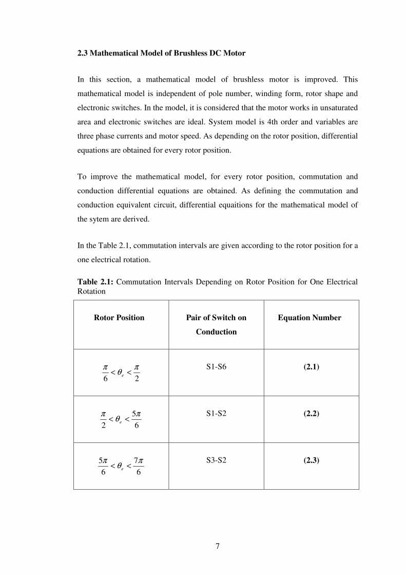
2.3 Mathematical Model of Brushless DC Motor
In this section, a mathematical model of brushless motor is improved. This
mathematical model is independent of pole number, winding form, rotor shape and
electronic switches. In the model, it is considered that the motor works in unsaturated
area and electronic switches are ideal. System model is 4th order and variables are
three phase currents and motor speed. As depending on the rotor position, differential
equations are obtained for every rotor position.
To improve the mathematical model, for every rotor position, commutation and
conduction differential equations are obtained. As defining the commutation and
conduction equivalent circuit, differential equaitions for the mathematical model of
the sytem are derived.
In the Table 2.1, commutation intervals are given according to the rotor position for a
one electrical rotation.
Table 2.1: Commutation Intervals Depending on Rotor Position for One Electrical Rotation
Rotor Position Pair of Switch on
Conduction
Equation Number
26
πθ
π<< e
S1-S6 (2.1)
6
5
2
πθ
π<< e
S1-S2 (2.2)
6
7
6
5 πθ
π<< e
S3-S2 (2.3)

8
2
3
6
7 πθ
π<< e
S3-S4 (2.4)
6
11
2
3 πθ
π<< e
S5-S4 (2.5)
66
11 πθ
π<< e
S5-S6 (2.6)
Here the passing from S5-S6 conduction step to S1-S6 step will be analysed as
improving the mathematical model of the system. Figure 2.5 and 2.6 show the
conduction (red arrow) and commutation (blue arrow) times respectively when the
rotor is positioned on 26
πθ
π<< e interval. As is seen in the figure, after finishing
the conduction of the C phase, A phase conduction is started. The commutation
circuit in this rotor position corresponds to the turning off C phase current equivalent
circuit. This equivalent circuit is valid until the C phase current becomes zero.
Figure 2.5: Conduction equivalent circuit for the 26
πθ
π<< e invertal
a
b
c
S2
S1 S3 S5
S4 S6
AR AL aE
BR
cR
BL
CL + -
Vd
bE
cE

9
Figure 2.6: Conduction equivalent circuit for the 26
πθ
π<< e invertal
The required differential equations are obtained by the help of conduction and
commutation equations and star node point equation. According to the star node
point equation, sum of the three phase currents is zero [12].
0=++ cba iii , CBA RRRR === , CBA LLLL === (2.7)
dt
diMLRiEE
dt
diMLRi b
bbc
c
c )()(0 +−−−+++= (2.8)
dt
diMLRiEE
dt
diMLRiV b
bba
a
ad )()( +−−−+++= (2.9)
From the 2.7 equation, replacing the C phase current on the 2.8 equation
[ ]bcab
ba EERiRiMLdt
di
dt
di+−+
+−−= .2
)(
12 (2.10)
is obtained. Derivative expression of the A phase current is replaced on 2.9 equation,
[ ]bcabd
b EEERiVMLdt
di23
)(3
1−++−−
+= (2.11)
is obtained. This equation consis of the, B phase current derivative expression, is
replaced on 2.10 equation
a
b
c
S2
S1 S3 S5
S4 S6
AR AL aE ai
bi
ci
BR
cR
BL
CL
+ Vd -
bE
cE

10
[ ]acbad
a EEERiVMLdt
di2.32
)(3
1−++−
+= (2.12)
is obtained. From the star node point equation,
0=++dt
di
dt
di
dt
di cba (2.13)
[ ]cbacd
c EEERiVMLdt
di23
)(3
1−++−−
+= (2.14)
C phase current derivative equation is obtained.
After the C phase current becomes zero, the Figure 2.5 circuit will be valid. While
conduction of S1-S6 switches, C phase current are zero thus star node point equation
is given by the 2.15 equation.
0=+ ba ii (2.15)
As considering the Fig. 2.6 circuit, if the A phase current is wrote as depending on
the B phase current,
( )[ ]babd
b EERiVMLdt
di−+−−
+= 2
2
1 (2.16)
[ ]abad
a EERiVMLdt
di−+−
+= 2
)(2
1 (2.17)
equations are obtained. 3.16 and 3.17 equations are defined as the phase current
equations of brushless DC motor system, for the 26
πθ
π<< e electrical rotor position
interval.

11
To complete the mathematical model of the system in this step, it is needed to write
the differential equations for mechanical side. Mechanical differential equations are
same for all the conduction steps and given as follow,
ωω
Bdt
dJMM ym +=− (2.18)
[ ]ωω)(
)(
1Ymym
ym
BBMMJJdt
d+−−
+= (2.19)
Instant torque value of brushless DC Motor is given by 2.20 equation.
ccbbaa ikikiktM ++=)( (2.20)
Electrical and mechanical equations for the other conduction steps can be obtained
by using the same method.
For the 6
5
2
πθ
π<< e rotor position interval, the commutation equations:
[ ])2(3)(3
1acbad
a kkkRiVMLdt
di−++−
+= ω (2.21)
[ ])2(3)(3
1bcabd
b kkkRiVMLdt
di−++−
+= ω (2.22)
[ ])2(32)(3
1cbacd
c kkkRiVMLdt
di−++−−
+= ω (2.23)
[ ]yccbbaa Mikikik
Jdt
d−++=
1ω (2.24)

12
For the 6
5
2
πθ
π<< e rotor position interval, the conduction equations:
[ ])(2)(2
1acad
a kkRiVMLdt
di−+−
+= ω ( 2.25)
0=bi (2.26)
[ ])(2)(2
1cacd
c kkRiVMLdt
di−+−−
+= ω (2.27)
[ ]yccaa Mikik
Jdt
d−+=
1ω (2.28)
For the 6
7
6
5 πθ
π<< e rotor position interval, the commutation equations:
[ ])2(3)(3
1acbad
a kkkRiVMLdt
di−++−−
+= ω (2.29)
[ ])2(32)(3
1bcabd
b kkkRiVMLdt
di−++−
+= ω (2.30)
[ ])2(3)(3
1cbacd
c kkkRiVMLdt
di−++−−
+= ω (2.31)
[ ]yccbbaa Mikikik
Jdt
d−++=
1ω (2.32)
For 6
7
6
5 πθ
π<< e rotor position interval, the conduction equations:
0=ai (2.33)
[ ])(2)(2
1bcbd
b kkRiVMLdt
di−+−
+= ω (2.34)

13
[ ])(2)(2
1cbcd
c kkRiVMLdt
di−+−−
+= ω (2.35)
[ ]yccbb Mikik
Jdt
d−+=
1ω (2.36)
For 2
3
6
5 πθ
π<< e rotor position interval, the commutation equations:
[ ])2(32)(3
1acbad
a kkkRiVMLdt
di−++−−
+= ω (2.37)
[ ])2(3)(3
1bcabd
b kkkRiVMLdt
di−++−
+= ω (2.38)
[ ])2(3)(3
1cbacd
c kkkRiVMLdt
di−++−
+= ω (2.39)
[ ]yccbbaa Mikikik
Jdt
d−++=
1ω (2.40)
For 2
3
6
5 πθ
π<< e rotor position interval, the conduction equations:
[ ])(2)(2
1abad
a kkRiVMLdt
di−+−−
+= ω (2.41)
[ ])(2)(2
1babd
b kkRiVMLdt
di−+−
+= ω (2.42)
0=ci (2.43)
[ ]ybbaa Mikik
Jdt
d−+=
1ω (2.44)

14
For 6
11
2
3 πθ
π<< e rotor position interval, the commutation equations:
[ ])2(3)(3
1acbad
a kkkRiVMLdt
di−++−−
+= ω (2.45)
[ ])2(3)(3
1bcabd
b kkkRiVMLdt
di−++−−
+= ω (2.46)
[ ])2(32)(3
1cbacd
c kkkRiVMLdt
di−++−
+= ω (2.47)
[ ]yccbbaa Mikikik
Jdt
d−++=
1ω (2.48)
For 6
11
2
3 πθ
π<< e rotor position interval, the conduction equations:
[ ])(2)(2
1acad
a kkRiVMLdt
di−+−−
+= ω (2.49)
0=bi (2.50)
[ ])(2)(2
1cbcd
c kkRiVMLdt
di−+−−
+= ω (2.51)
[ ]yccaa Mikik
Jdt
d−+=
1ω (2.52)
For 66
11 πθ
π<< e rotor position interval, the commutation equations:
[ ])2(3)(3
1acbad
a kkkRiVMLdt
di−++−
+= ω (2.53)

15
[ ])2(32)(3
1bcabd
b kkkRiVMLdt
di−++−−
+= ω (2.54)
[ ])2(3)(3
1cbacd
c kkkRiVMLdt
di−++−
+= ω (2.55)
[ ]yccbbaa Mikikik
Jdt
d−++=
1ω (2.56)
For 66
11 πθ
π<< e rotor position interval, the conduction equations:
0=ai (2.57)
[ ])(2)(2
1bcbd
b kkRiVMLdt
di−+−−
+= ω (2.58)
[ ])(2)(2
1cbcd
c kkRiVMLdt
di−+−−
+= ω (2.59)
[ ]yccbb Mikik
Jdt
d−+=
1ω (2.60)
To complete the mathematical model of the system, it is needed to express induced
voltage on every phase for every conduction step. If star point is considered
reference point, the instant value of the induced voltage is the function of motor
constant, angular rotor velocity and rotor position. Motor constant depends on rotor
position in brushless dc motor. In this concept, induced voltage on the phase
windings for the unit velocity is improved in accordance with general mathematical
model expression.
Motor constant change for A phase:
αθ << e0 α
θ e
a
kk = (2.61)

16
)(0 βαθ +<< e kka = (2.62)
)()( απθβα +<<+ e α
πθ )( −−= e
a
kk (2.63)
)()( βαπθαπ ++<<+ e kka −= (2.64)
πθβαπ 2)( <<++ e α
πθ )2( −= e
a
kk (2.65)
Motor constant change for B phase:
απ
θ −<<3
20 e kkb −= (2.66)
βαπ
θαπ
−−<<−3
5
3
2e
α
πθ )
3
2( −
=e
b
k
k (2.67)
απ
θβαπ
−<<−−3
5
3
5e kkb = (2.68)
βαπ
θαπ
−−<<−3
8
3
5e
α
πθ )
3
5( −−
=e
b
k
k (2.69)
πθβαπ
23
8<<−− e kkb −= (2.70)
Motor constant change for C phase:
απ
θ −<<3
0 e kkc = (2.71)
βαπ
θαπ
−−<<−3
4
3e
α
πθ )
3( −−
=e
c
k
k (2.72)

17
απ
θβαπ
−<<−−3
4
3
4e kkc −= (2.73)
βαπ
θαπ
−−<<−3
7
3
4e
α
πθ )
3
4( −
=e
c
k
k (2.74)
πθβαπ
23
7<<−− e kkc = (2.75)
2.4 Torque Equation of Brushless DC Motor
To explain the torque generation of brushless DC motors, it is necessary to
understand the characteristics of movement voltages induced on stator windings [12].
Magnetic Flux induced on just one coil is given by:
)2/2/(,)( πθππψ ≤≤−= mBrl (2.76)
The Movement Voltage induced on the coil:
rm
rm lrBrlB
dt
d
d
d
dt
de ω
π
ωπθ
θ
ψψ2
2/. ==== (2.77)
r
r
dt
dω
θ= , re pθθ = (2.78)
are obtained. Total EMF induced on stator windings given by the following equation:
rmlrNBE ω2= (2.79)
and the Torque generated by a brushless DC motor is given analytical as follow,
r
ccbbaa
total
iEiEiEM
ω
++= (2.80)

18
r
r
ytotal Bdt
dJMM ω
ω+=− (2.81)
2.5 Fundemental of BLDC Motor Operation
To simplify the explanation of how to operate a three-phase BLDC motor, we may
consider that BLDC motor has only three coils. To make the motor rotate, for each
commutation sequence one of the three windings energized by positive power
(current enters into the winding), the second winding is negative (current exits the
winding) and the third one is non-energized condition. Torque is produced because
of the interaction between the magnetic field generated by the stator coils and the
permanent magnets of the rotor. The magnetic field attracts and rejects the permanent
magnets of the rotor. In order to keep the motor running, the magnetic field produced
by the stator windings sequence should change thus the rotor rotates to catch up with
the stator magnetic field. By changing the current flow in the coils, the polarity of the
magnetic fields change at the right moment and the motor rotates. Ideally, the peak
torque occurs when the angle of these two fields are at 90° .

19
3. BLDC MOTOR CONTROL
3.1 Torque-Speed Quadrants Concept
DC motor controls can be classified by the quadrants of operation referring to the
torque versus speed plot. In this respect, there are four quadrants control. (See the Fig
3.1)
Figure 3.1: Torque/Speed Quadrant of Operation.
3.1.1 One-Quadrant Control
Single - quadrant controls only operate in the first quadrant with positive speed and
positive torque. A single quadrant drive usually consists of a single transistor and a
single clamp diode. This type of control can only move the motor in one direction
and cannot generate any braking forces. [3]
First Quadrant Positive Speed, Positive Torque, ”Forward- Accelerating”
I
Second Quadrant Negative Speed, Positive Torque, ”Reverse Braking”
II III Third Quadrant Negative Speed, Negative Torque, ”Reverse-Accelerating”
IV Fourth Quadrant Positive Speed, Negative Torque, ”Forward-Braking”
20
3.1.2 Two-Quadrant Control
The most widely used control method for BLDC motors is the 2 Quadrant Speed
(Voltage) control. In the two-quadrant control you can not generate any braking
forces. The motor can only operate in quadrant I (forward accelerating) and quadrant
III (reverse accelerating). In order to reverse the directions of the rotor, the motor
must coast down to zero before reversing directions. If the average applied voltage is
less than the back EMF of the motor, the motor current will decrease to zero and the
motor will coast. If there is no friction, the motor may spin forever. Many loads, such
as fans or pumps, are mostly frictional. Two quadrant control can be easly used in
these systems. In a six steps drive system, to implement 2 quadrant speed control it is
sufficient to implement PWM only the bottom power switches in the power inverter
(See Fig. 3.2). In this case, a 0-100% PWM duty cycle adjusts the average voltage
applied to the motor and creates a controlled minimum to maximum Speed range. As
the average applied voltage increases, motor current increases to accelerate the
motor. As motor speed increases its back EMF voltage increases proportionally, but
opposes to the applied voltage. In 2-Quadrant Voltage control applications, the top
power switches are opened and closed at the commutation frequency which is
proportional to (n x P)/60, where n is motor speed in rpm and P is the number of pole
pairs. As an example, a 6000min–1, 16 pole (8 pole-pair) motor will have a
commutation frequency of (6000 x 8)/60 = 800 Hz maximum. The bottom switches
must operate at the PWM switching frequency (typically 20kHz). Since both
switching losses and power switch gate drive requirements increase with switching
frequency, not having to PWM on the top switches results in Higher Operating
Efficiency. The top gate drive circuitry is also simpler than the bottom gate drive
circuitry.
2-Quadrant operating BLDC motor can be reversed by reversing the Electronic
Commutator switching sequence. However, this cannot be done quickly because the
motor current is not directly controlled (the motor voltage is controlled). In a 2-
Quadrant control configuration, the motor must coast to decrease speed. The actions
like controlled deceleration (dynamic braking), hard reversal rotation as required by
a typical servo application, can be achieved by operating the BLDC motor with a 4-
Quadrant BLDC controller.

21
Figure 3.2: Six-Step Drive System for BLDC Motor.
3.1.3 Four-Quadrant Control
4-Quadrant Squarewave BLDC controller is operated with an internal current
(Torque) control loop. In a 4-Quadrant Power Inverter, both the top and bottom
power switches are simultaneously Pulse-Width-Modulated. During the PWM OFF
cycle, the current in the power inverter freewheel backwards-through the anti-parallel
connected power diodes, and a the DC bus capacitor. The current flows in the same
shunt, but in the opposite direction to the current during the PWM ON cycle. Thus, a
continuous feedback signal proportional to current (Torque) is obtained by sensing
the shunt voltage with a current sense amplifier that also detects the absolute value of
the current signal. This signal is then subtracted from an external current reference
(Torque or current command signal) and the resultant current loop error signal is
amplified and used to control the PWM modulator. Hence, the motor current
(Torque) is controlled directly.
The Power losses in the 4-Quadrant control are higher than in the 2-Quadrant since
all power switches are Pulse - Width-Modulated as discussed above. In 4-Quadrant
controllers, a Dynamic Braking resistor and transistor (usually connected in series
across the DC bus) is used to absorb the kinetic energy released by the motor during
rapid deceleration and hard reversing. The released kinetic energy appears as a
reverse current flowing out from the Power Inverter into the DC bus capacitor,
through the flyback diodes connected in anti-parallel with each Inverter power
switch. This reverse (braking) current charges the bus capacitor, increasing the
average DC bus voltage. A Dynamic Braking control circuit must sense this excess
a
b
c
S2
S1 S3 S5
S4 S6
AR AL aE

22
DC bus voltage and properly switch the Dynamic Braking transistor across the DC
bus in order to bound the DC bus voltage to safe operating levels. When the braking
transistor Turns-ON, power is dissipated in the braking resistor proportional to
braking resistance times the square of the RMS braking current. The excess kinetic
energy is converted to heat dissipated by the braking resistor while, the DC bus is
simultaneously maintained at a safe DC operating level [4].
3.2 Closed Loop Speed Control Theory
Commutation provide the proper rotor rotation of the BLDC motor, while the motor
speed only depends on the amplitude of the applied voltage. The amplitude of the
applied voltage is adjusted using the PWM technique.
The required speed is controlled by a speed controller, which is performed
proportional-integral (PI) controller. To generate a voltage proportional to desired
speed, the difference between the actual and required speeds is fed to input of the PI
controller and setted the duty cycle of the PWM pulses (See Fig. 3.3.)
Figure 3.3: Speed Controller
The speed controller calculates the PI algorithm given in the equation below:
ç0
])(1
+)([=)(t
I
C dtteT
teKtu (3.1)

23
After transforming the equation into a discrete time domain using an integral
approximation with the Backward Euler method, it is obtained the following
equations for the numerical PI controller calculation:
)(.+)1(=)(
)(.=)(
)(+)(=)(
keT
TKkuku
keKku
kukuku
I
CII
Cp
Ip
(3.2)
Where:
k stepin output Controller = u(k)
k stepin valueMeasured=m(k)
k stepin valueDesired=w(k)
k stepin error Input =)(ke
gain Controller = K
timeSampling = T
constant timeIntegral = T
1-k stepin portion output Integral = 1)-(ku
k stepin portion output Integral = (k)u
k stepin portion output alProportion=(k)u
C
I
I
I
p
3.3 Digital Control
The BLDC motor is driven by rectangular voltage pulses according to the given rotor
position (see Figure 3.4). Rotor flux generated by the rotor magnet intersect with the
generated stator flux thus created a torque that defines the speed of the motor. Rotor
flux is generated by a rotor magnet and defines the torque and thus the speed of the
motor as mentioned before. The voltage pulses must be properly applied to the
phases of the three-phase winding system so that the angle between the stator flux
and the rotor flux is kept as close to 90° as possible, to get the maximum generated
torque. Therefore, the motor requires electronic control for proper operation.

24
Figure 3.4: Voltage Strokes Applied to the 3-Phase BLDC Motor.
For the 3-phase BLDC motors, a standard 3-phase power stage is used (see Figure
3.5). The power stage consist of six power transistors. In both modes, the 3-phase
power stage energizes two motor phases simultaneously. The third phase is
nonenergised. Thus, it is obtained six possible voltage vectors that are applied to the
BLDC motor using a pulse width modulation (PWM) technique.
Figure 3.5: 3-Phase BLDC Power Stage.
Phase A Phase B Phase C
a b
Q2 Q6
PWM_Q1
PWM_Q6 PWM_Q4
PWM_Q5 PWM_Q3
PWM_Q2
GND
c
Q4
DCBV
Q1 Q3 Q5

25
4. CLOSED LOOP SPEED CONTROL DRIVER
4.1 Driver Construction
The main difficulty for control BLDC motors is to decode data coming from Hall
effect sensors and perform some important functions like forward/reverse selection,
overcurrent shutdown, undervoltage lockout, overtemperature shutdown. It is
possible to use discrete components to perform these functions but it means too much
circuit board area, especially if the control unit is to be placed inside the motor.
Another problem is insufficient performance of the existing power transistors. Power
bipolars can not be favored because they can not be driven directly from a control IC
and here power MOSFETs may be the best choice since they are easy to drive,
efficient and cheaper.
As explained in the following sections with the details, three main devices undirlies
our control circuit. MC33035 is the brain IC of the circuit and control all the
operation. MC33039 is the closed−loop speed control IC (electronic tachometer) give
the speed information of the rotor and lastly MSK3003 is a three phase bridge
inverter electronicly comutate the motor and make the control easier.
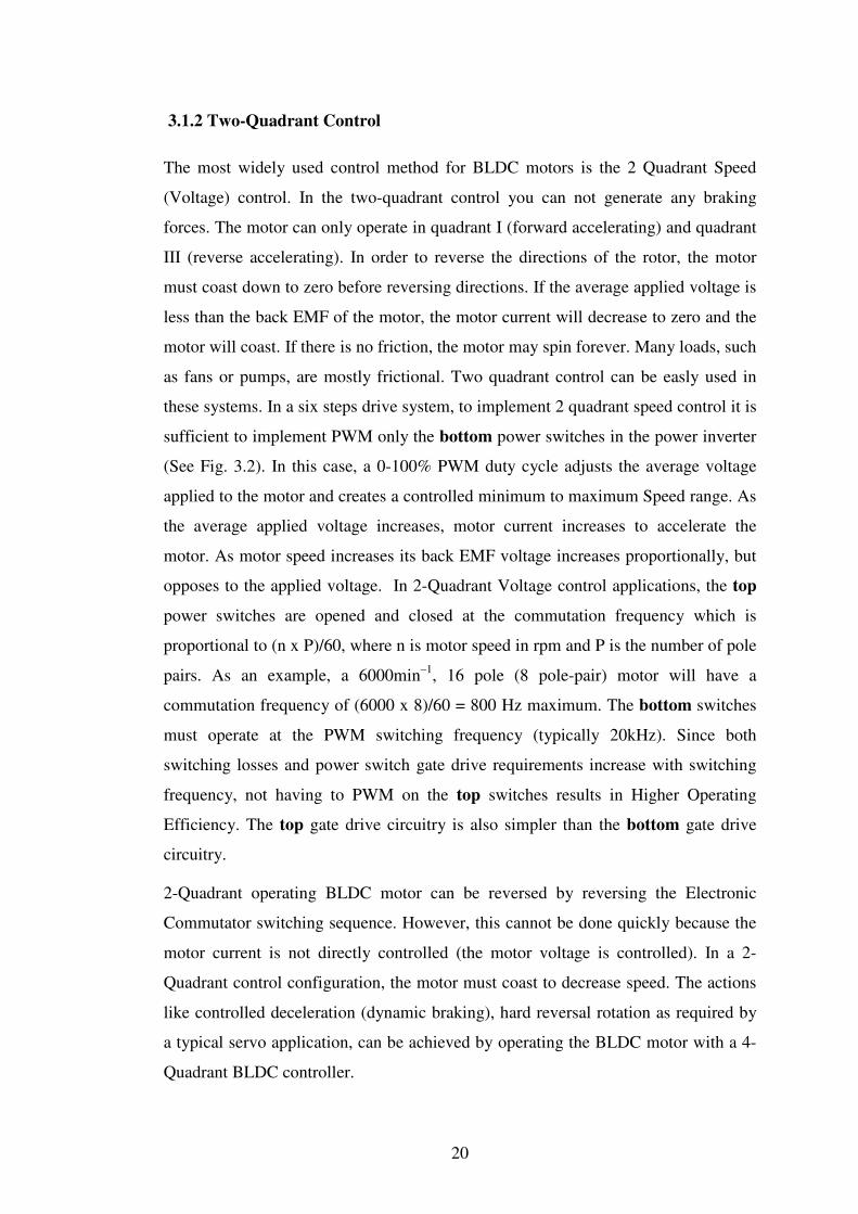
4.1.1 MC 33035 IC
The MC33035 is a brushless DC motor controller IC can perform all of the active
functions mentioned above. This IC has a rotor position decoder to provide proper
commutation, sawtooth oscillator, three open collector top drivers and three totem
pole bottom drivers suited for driving power MOSFETs (See Fig. 4.1 and Fig. 4.2).
MC33035 has the following features:
• 10 to 30 V Operation
• Undervoltage Lockout

26
• 6.25 V Reference Capable of Supplying Sensor Power
• Fully Accessible Error Amplifier for Closed Loop Servo Applications
• High Current Drivers Can Control External 3−Phase MOSFET Bridge
• Cycle−By−Cycle Current Limiting
• Pinned−Out Current Sense Reference
• Internal Thermal Shutdown
• Selectable 60°/300° or 120°/240° Sensor Phasings
• Can Efficiently Control Brush DC Motors with External MOSFET H−Bridge
Figure 4.1: MC33035 Pin Connections [6]
27
Figure 4.2: MC33035 Representative Block Diagram [6]

28
PIN SYMBOL DESCRIPTION
1,2,24 TTT CAB ,, These three open collector Top drive outputs are designed to
drive the external upper power switch transistors.
3 Fwd/Rev The Forward/Reverse Input is used to change the direction of motor rotation.
4, 5, 6 CBA SSS ,, These three Sensor Inputs control the commutation sequence.
7 Output Enable A logic high at this input causes the motor to run, while a low
causes it to coast.
8 Reference Output This output provides charging current for the oscillator timing
capacitor TC and a reference for the error amplifier. It may
also serve to furnish sensor power.
9 Current Sense
Noninverting input
A 100mV signal, with respect to Pin 15, at this input terminates output switch conductioın during a given oscillator cycle. This pin normally connects to the top side of the current sense resistor.
10 Oscillator The Oscillator frequency is programmed by the values selected
for the timing components, TT CR , .
11 Error Amp
Noninverting Input
This input is normally connected to the speed set potentiometer.
12 Error Amp Inverting
Input
This input is normally connected to the Error Amp Output in open loop applications.
13 Error Amp Out/PWM
Input
This pin is available for compensation in closed loop applications.
14 Fault Output This open collector output is active low during one or more of the following conditions: Invalid Sensor Input code, Enable Input at logic 0, Current Sense Input greater than 100 mV (Pin 9 with respect to Pin 15), Undervoltage Lockout activation, and Thermal Shutdown.
15 Current Sense Inverting
Input
Reference pin for internal 100 mV threshold. This pin is normally connected to the bottom side of the current sense resistor.
16 Gnd This pin supplies a ground for the control circuit and should be referenced back to the power source ground.
17 CCV This pin is the positive supply of the control IC. The controller
is functional over a minimum VCC range of 10 to 30 V. 18
CV The high state (VOH) of the Bottom Drive Outputs is set by the voltage applied to this pin. The controller is operational over a minimum VC range of 10 to 30 V.
19, 20, 21 BBB ABC ,, These three totem pole Bottom Drive Outputs are designed for
direct drive of the external bottom power switch transistors. 22 00 12060 Select The electrical state of this pin configures the control circuit
operation for either 60° (high state) or 120° (low state) sensor electrical phasing inputs.
23 Brake A logic low state at this input allows the motor to run, while a high state does not allow motor operation and if operating causes rapid deceleration.
Table 4.1: MC33035 Pin Descriptions

29
4.1.1.1 Rotor Position Decoder
The main duty of the rotor position decoder is to decode signals coming from Hall
Effect Sensors and to provide proper sequencing for the top and bottom drive
outputs. Here the inputs are TTL (Transistor-Transistor Logic) compatible, with their
thresholds typically at 2.2 V. That means 0.0 – 0.8 V correspond to logic 0 and 2.2-
5V correspond to logic 1. Details of rotor position decoder will be discussed in
commutation process.
4.1.1.2 Error Amplifier
An important structure is a high performance internal error amplifier is designed as
unity gain voltage follower that is porssible to access to both inputs and output (Pins
11, 12, 13). This structure enables open and closed loop speed control. In the
following figure, error amplifier output is connected to the PWM input.
Figure 4.3: Error Amplifier [5]
4.1.1.3 Oscillator
Duty of the oscillator is to set the both R-S flip flop and thus control the conduction
of the top and bottom drive outputs. The frequency of the oscillator is setted by the
timing components RT(R2) and CT(C2) (See Fig. 4.8). Capacitor CT is charged from
the MC33035 Reference Output (Pin 8) through resistor RT and discharged by an
internal transistor.

30
4.1.1.4 Pulse Width Modulator
It’s a good and energy efficient method to control the speed of the motor as varying
pulse widths of the applied voltage to each stator windings during the commutation.
Here as CT (C2) discharges, the sawtooth oscillator adjusts both latches and control
the top and bottom drive outputs. When positive rising voltage of CT becomes higher
than the error amplifier output, the PWM comparator cut off the bottom drive output
transmission as reseting the upper latch. Pulse width modulation is performed only at
the bottom drive outputs. The pulse width modulator timing diagram is shown in
Figure 4.4.
Figure 4.4: Pulse Width Modulator Timing Diagram [5]
4.1.2 MC33039 ElectronicTachometer
The MC33039 is an electronic tachometer can perform closed−loop speed control of
a brushless DC motor as coorporating with MC33035. This part consists of three
input buffers, three digital edge detectors, a programmable monostable and an
internal shunt regulator. This device can be used in many closed-loop speed control
applications. Refer to Figure 4.5 for the block diagram.

31
Figure 4.5: MC33039 Block Diagram [7]
4.1.3 MSK3003 Power Module
The MSK3003 is a three phase bridge power module consisting of P-Channel
MOSFETs for the top transistors and N-Channel MOSFETs for the bottom
transistors. The MSK3003 can be used directly with many brushless motor drive IC's
without additional circuits. Refer to Figure 4.6 for the MSK3003 circuit schematic.
Figure 4.6: MSK3003 Circuit Scheme

32
4.2 Assembyling the Circuit
4.2.1 Timing Components
The brushless DC motor used in this project has one pair of pole on its permanent
magnet and there is one electrical degree for every mechanical degree. Each Hall
effect sensor generates one pulse and the three sensors generate three pulses for
every mechanical revolution. MC33039 generates one pulse for every rising and
falling edge and totally generates 6 pulses.
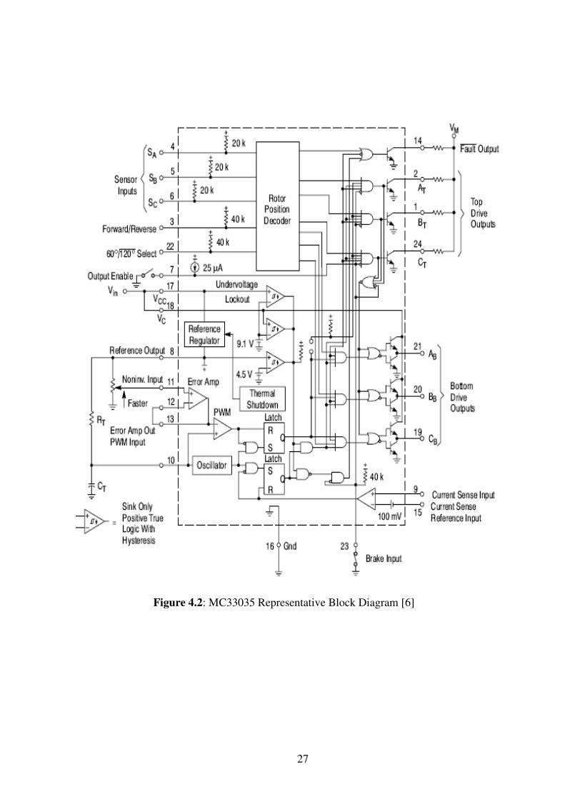
In Fig 4.8 R1 and C1 are the MC33039 timing components and the values of C1 and
R1 set the outf pulse width which takes the maximum value for a given maximum
speed. Figure 4.7 shows the MC33039 timing diagram. The timing components are
selected according to the desired maximum motor RPM.
R2 and C2 on Figure 4.8 are the timing components for the MC33035. Capacitor C2
(CT) is charged from the Reference Output (Pin 8) through resistor R2 (RT) and
discharged by an internal transistor as mentioned before in chapter 4.1.1.3. The
values of the timing components set the frequency of the internal ramp oscillator.
4.2.2 Drive Circuits
MC33035 has six output drivers. Three top drive outputs open collector NPN
transistors (Pins 1, 2, 24) drive the P-Channel MOSFETs. Three totem pole bottom
drive outputs (Pins 19, 20, 21) can drive directly N−Channel MOSFETs. Bottom
drive outputs are supplied from from VC (Pin 18) as being independent source of
VCC. While VCC is greather than 20V, MOSFETs gates might damage, therefore a
zener diode must be connected to Pin 18.
33
Figure 4.7: Timing Diagram of A Typical Three Phase, Six Step Motor Application
[6]

34
4.2.2.1 N-Channel Gate Drive Circuit
If that considered our system supplied from 24V (18 to 30V), MC33035 can be
powered directly from system voltage since the IC has a 40 V rating. Here with the
electrolytic capacitor (C8), a small filter capacitor (C7 - 0.1µF) is placed close the IC
to minimize local spiking across the DC bus.
To minimize the power losses in the IC, three lower output transistors are driven with
a seperate supply (VC-Pin18) from the MC33035. The required current to drive the
MOSFETs is just the current to charge and discharge the gate-to-source and drain-to-
gate capacitors of each MOSFET. C4 filter capacitor supplies the turn-on current
while refrehsed through resistor R7 because the MOSFETs draw very small average
current and high current values are required to charge their input capacitances.
Dropping resistor (R7) gets 3 V when the main supply takes the lowest value 18 V in
the 24 V system. For charging the capacitor it’s a good selection to use a 1 kΩ
resistor, it will also supply at least 1 mA current to the zener to provide good
regulation. At high supply voltages the resistor will see a voltage of 15 V, a current
of 15 mA, and it means to a power dissipation about 0.25 W. Therefore, a 0.5 W
resistor will be a good choice. That’s also a good power rating for the zener. Also
three Schottky diodes D1, D2, D3 are placed between the Gates of the N-Channel
MOSFETs and the ground to prevent the rupture if the substrate current exceeds
50mA.
If the gate drive impedance of the three lower devices is low it may be the problem
that gate drive loop may cause ringing during gate voltage transitions. Such a ringing
is amplified by the MOSFETs and may occures high levels of noise at the drain. It
may be the solution to insert the series resistance to gate drive as reducing the
circuit’s Q. Any gate drive resistor value lower than 62 Ω may occur oscillations in
this circuit. (See Fig.4.8)
4.2.2.2 P-Channel Gate Drive Circuit
At least 7 - 8 V may be acceptable on gates for standard MOSFETs. R5 and R6 are
selected to provide that the P channel gate drives take 10 V value even if the supply
voltage gets lowest value (18 V). R5, 12 and 13 control turn-on speed as providing
keep charged of the P-channel input capacitances. Similarly, R6, R14 and R15
control turn-off speed. Since P-channels MOSFETs work at the same frequency with

35
the motor comutation frequeny (lower than the PWM frequency), it’s not required
the low impedance for P-Channel gate drives.
Figure 4.8: Closed Loop Brushless DC Motor Control Using The MC33035,
MC33039, MSK3003 [6]
4.3 Control Features
The MC33035 is not capable of closed loop speed control. The IC can not monitor
the motor speed and generates a signal proportional to the motor RPM, generally
performed by a tachometer. If the motor speed signal is provided, MC33035 can
manage closed loop speed control application.
4.3.1 Open Loop Speed Control
It’s not required to know motor speed data to perform open loop control. It is enough
to give a signal proportional to desired motor speed into the error amplifier’s non–
inverting input (Pin 11). Then output of the error amplifier is compared to the output

36
of the oscillator to obtain a PWM signal proportional to desired motor speed until the
control loop is terminated by an overcurrent or fault condition.
4.3.2 Closed Loop Speed Control
For closed loop motor speed control, the MC33035 requires an input voltage
proportional to the motor speed. This input voltage is generated by the MC33039.
Figure 4.8 shows the application that 6.25 V reference from the MC33035 (Pin 8) is
supplied to the MC33039 used to generate the feedback voltage proportional to the
motor speed without need a tachometer. The both MC33035 and MC33039 use the
same Hall sensor signals. Altough MC33035 use them to decode rotor position,
MC33039 use Hall sensor signals to detect the speed of the rotor.
With every rising and falling edge of the Hall sensor signals, MC33039 generates an
output pulse which its amplitude and time duration are setted by the values of the
resistor R1 and the capacitor C1. These output pulses released from MC33039 ( Pin 5)
are integrated by the error amplifier of the MC33035 and generated a DC voltage
level proportional to motor speed.
After generating a signal proportional to motor speed, this signal set the PWM
reference level at Pin 13 of the MC33035 and closes the last major link of the
feedback loop and the signal is fed into the inverting input (Pin 12) of the
MC33035’s comparator. Here the MC33039’s output is low pass filtered by the R4,
C3. The signal proportional to desired motor speed drives the non–inverting input
(Pin 11) and the ratio of the input and feedback resistors R3 and R4 control the gain.
Here feedback capacitor C3 combines the low pass filtering and generating the error
signal.
MC33035 expands the output pulse width to the drive transistors if the motor speed
becomes lower than the desired speed, inversly the duty cycle decreases if the motor
speed is greater than the desired speed. If the desired speed is so much lower than the
motor speed, the duty cycle fall to zero and the motor would coast to desired speed.

37
Figure 4.9: The Functional Block Diagram of the System
Actual Speed Signal
MC33039 Tacho IC
POWER MODULE
Hall Effect Sensors
MC33035 Controller + Decoder
Gate Signals
Hall Sensor Signals
Reference Speed Signal
POWER SOURCE
BRUSHLESS DC MOTOR
Energizing Signals (voltage)

38
4.4 Commutation
4.4.1 Rotor Position Decoder
Corresponding to three sensor inputs, eight possible input code combinations
available and two of them are invalid inputs codes that are there are six valid input
codes. The decoder can define the rotor position using the six valid input codes. The
direction of motor rotation can be changed by the Forward/Reverse input (Pin 3) as
giving a reverse voltage to the stator winding. The commutation sequence is reversed
when the input changes from high to low with a given sensor input code the active
top and bottom drive outputs are exchanged (AT to AB, BT to BB, CT to CB).
Consequently the motor changes directional rotation. The Output Enable pin (Pin 7)
controls the on/off state of the motor. 25 mA current source provide sequencing of
the top and bottom drive outputs when the pin left disconnected. When grounded, the
motor coast as turning off the top drive outputs and forcing low the bottom drives
and the Fault output activates. Braking is performed by setting the Brake Input (Pin
23) in a high state. Thus the top drive outputs turn off and the bottom drives turn on
as shorting the motor windings and generating back EMF. The brake input has
unconditional priority over all other inputs.
4.4.2 Commutation Process
The comutation decoder of the MC33035 receives signals from the position sensors
regarding the position of the rotor and translates them into the switching signals as
supplying to the firing circuit consist of the electronic switches. In a six step drive
system, two switches are activated simultaniously to energise two of the stator phase
and a rotating field is established in the air-gap by the interaction of the currents on
the two coils.
39
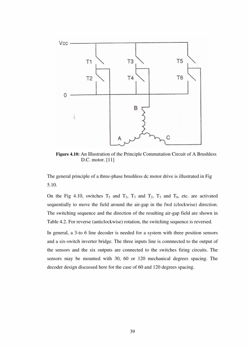
Figure 4.10: An Illustration of the Principle Commutation Circuit of A Brushless D.C. motor. [11]
The general principle of a three-phase brushless dc motor drive is illustrated in Fig
5.10.
On the Fig 4.10, switches T5 and T2, T3 and T2, T3 and T6, etc. are activated
sequentially to move the field around the air-gap in the fwd (clockwise) direction.
The switching sequence and the direction of the resulting air-gap field are shown in
Table 4.2. For reverse (anticlockwise) rotation, the switching sequence is reversed.
In general, a 3-to 6 line decoder is needed for a system with three position sensors
and a six-switch inverter bridge. The three inputs line is connnected to the output of
the sensors and the six outputs are connected to the switches firing circuits. The
sensors may be mounted with 30, 60 or 120 mechanical degrees spacing. The
decoder design discussed here for the case of 60 and 120 degrees spacing.

40
Table 4.2: Switching Sequence and Resulting Air-Gap Field Direction [11]
Figure 4.11: Four - Poles Permanent Magnet Rotor and Three Sensors Spacing at 60
Degrees [11]

41
Schematic of the four poles permanent magnet rotor and the position sensors is
shown in Fig 5.11. Each sensor generate high (logic 1) pulse when it is passed by a
South pole and low (logic 0) when it is passed by a North pole. For the initial
position shown in Fig 4.11, the first sensor (H1) operates at 00 the second (H2)
operates after 060 and the third (H3) releases after 030 of rotation in the clockwise
(forward) direction. Table 4.3 is the comutation truth table and shows the sensor
ouput code for forward and reverse rotation. There are six different commutation
logic combinations per one electrical revolution and the logic codes for both
directions are the same, but the code sequence is reversed.
The decoder truth table is readily derived with the aid of Table 4.2, Fig.4.11 and
4.12. In order to enable rotation to both directions, a code corresponding to the
desired direction of rotation (F/R select) is added as an input to the commutation
decoder. Here codes 1 and 0 are chosen for forward (clockwise) and backward
rotation respectively, but this is arbitrary. Other inputs to the commutation decoder
are sensors output codes, Output Enable code (Pin 7), brake input (Pin 23), Curren
Sense input and 00 12060 sensor phase selection. The commutation decoder truth
table is given with the Table 4.3.
The Boolean functions of the semiconductor switches are as follows:
)3.2.()3.2.(=3
)2.1.()2.1.(=2
)2.1.()2.1.(=1
HHRHHFT
HHRHHFT
HHRHHFT
(4.1)
.)1.3.()1.3.(=6
)1.3.()1.3.(=5
)3.2.()3.2.(=4
HHRHHFT
HHRHHFT
HHRHHFT
(4.2)

42
Figure 4.12: Three Phase, Six Step, Full Wave Commutation Waveforms [6]

43
Table 4.3: Three Phase Six Step Commutation Truth Table
Sensor Electrical Phasing Top Drives Bottom
Drives
60 0
AS BS CS
0120
AS BS CS
F/R Enable Brake
TA
TB
TC
BA
BB
BC
Fault
Active
Switches
1 0 0 1 0 0 1 1 0 0 0 1 1 0 0 1 1 T5, T2
1 1 0 1 1 0 1 1 0 0 1 0 1 0 0 1 1 T3, T2
1 1 1 0 1 0 1 1 0 0 1 0 1 1 0 0 1 T3, T6
0 1 1 0 1 1 1 1 0 0 1 1 0 1 0 0 1 T1, T6
0 0 1 0 0 1 1 1 0 0 1 1 0 0 1 0 1 T1, T4
0 0 0 1 0 1 1 1 0 0 0 1 1 0 1 0 1 T5, T4
1 0 0 1 0 0 0 1 0 0 1 1 0 1 0 0 1 T1, T6
1 1 0 1 1 0 0 1 0 0 1 1 0 0 1 0 1 T1, T4
1 1 1 0 1 0 0 1 0 0 0 1 1 0 1 0 1 T5, T4
Current Sense

44
0 1 1 0 1 1 0 1 0 0 0 1 1 0 0 1 1 T5, T2
0 0 1 0 0 1 0 1 0 0 1 0 1 0 0 1 1 T3, T2
0 0 0 1 0 1 0 1 0 0 1 0 1 1 0 0 1 T3, T6
1 0 1 1 1 1 X X 0 X 1 1 1 0 0 0 0 ___
0 1 0 0 0 0 X X 0 X 1 1 1 0 0 0 0 ___
1 0 1 1 1 1 X X 1 X 1 1 1 1 1 1 0 T2,T4,T6
0 1 0 0 0 0 X X 1 X 1 1 1 1 1 1 0 T2,T4,T6
V V V V V V X 1 1 X 1 1 1 1 1 1 1 T2,T4,T6
V V V V V V X 0 1 X 1 1 1 1 1 1 0 T2,T4,T6
V V V V V V X 0 0 X 1 1 1 0 0 0 0 ___
V V V V V V X 1 0 1 1 1 1 0 0 0 0 ___

45
4.5 Fault Management
The duty of the open collector Fault Output (Pin 14) is alerting the IC in the event of
the system malfunction. It pulls the Fault Output Pin “low” as supplying maximum 16
mA current when the system has any fault condition and can directly drive a LED for
visual indication thus alert the IC for a problemis. Here R11 (See Fig. 4.8) takes the
2.2 k values in a 24 V system to supply 1 mA to the LED. Upon fault detection, it is
suitable to terminate any further pulsing to the output transistors. This is possible by
connecting the Fault Output to the Enable pin (Pin 7). Thus the motor start up cırrent
is limitted or latched the system off. It is possible to create a time − delayed latched
shutdown for overcurrent condition as inserting of a RC (R10 and C6, see Fig. 4.8)
network between the Fault Output (Pin 14) and the enable input (Pin 7). Here is the
latch can be delayed by inserting C6 (47µF). The delay is setted by the time constant of
R10 and C6 before the system latches. The Fault Output is active low when one or more
of the following conditions occur:
1) Invalid Sensor Input code
2) Output Enable at logic [0]
3) Current Sense Input greater than 100 mV
4) Undervoltage Lockout
5) Thermal Shutdown
4.5.1 Over Current Detection
An over−current condition may occur while continuous operation of the motor that is
severely results in overheating and eventual failure. If the pulse width is increased
abruptly to quickly accelerate the motor, very high currents may flow. This will cause
an undesirable jerk on the motor and the mechanical system. Worse, it could exceed
the current rating of the power devices.
4.5.1.1 Overcurrent Sensing
The excessive load currents are detected by the comparator of MC33035. A signal
related with all the N-channel sources is fed into a comparator from the current
sensing resistor (R21). Here the trip threshold is 100 mV. The comparator then feeds

46
the RS Flip–Flop and if an overcurrent condition is detected, the output drivers turn –
off the power transistors the remainder of the oscillator cycle. In here, R21 is the
current sensing resistor 0.05 Ω and has 1W power rating and the sense voltage is
reduced by a voltage divider. The voltage divider values are, 100Ω (R8 in Figure 4.8)
for the upper resistor and 33Ω (R9) for the lower one that set the trip currnet to 8A. To
preserve the overcurrent comparator from noise or currents such as reverse recovery
spikes of freewheeling diyotes replacing a small capacitor (C5). It is easy to see that
the DC gain of the network is set by the resistive divider, but the time constant may
not be obvious at a glance. The transfer function for the resistive divider network and
the capacitor is calculated as follow:
In the s domain analysis a capacitance C is replaced by an admitance sC, or
equivalently an impedance 1/sC,
98598
9
59
98
59
9
98
90
++...=
1+..+
1+..=
)//(+
//==)(
5
5
RRCsRR
R
CsR
RR
CsR
R
ZRR
ZR
V
VsT
C
C
i
(4.3)
t
RRC
RR
eRRC
R
RRCsRR
RLsTLtT
...
+
985
9
98598
911 985
98
...
=++...
=)(=)( (4.4)
where Vi is the voltage across the current sense resistor and Vo is the voltage
appearing at the input of the comparator. In this case τ is 2.4 µs.
4.5.1.2 Current Limiting
Limiting the rate of acceleration is a fairly simple task for an IC. However, a simple
rate limit moy not protect the MOSFETs under an overvurrent condition. This
destructive condition can be best prevented with the use of cycle−by−cycle current
limiting. Cycle−by−cycle current limiting is accomplished by monitoring the stator
current. While the current is building−up an output switch conducts each time, and
upon sensing an over current condition, immediately turned off the switch and holded
it off for the remaining duration of the oscillator ramp−up period. The stator current is
converted to a voltage by inserting a grounded sense resistor RS (R21) (See Figure 4.8)
in series with the three bottom switch transistors (Q4, Q5, Q6). The sense voltage,

47
which is proportional to load current, is fed into a comparator (Pin 9) on board the
MC33035. Then this voltage is monitored by the current sense input (Pin 9 and Pin 15)
and compared to the internal 100 mV reference. If the 100 mV current sense threshold
is exceeded, the comparator resets the lower sense latch (RS Flip–Flop) and the output
drivers turn–off the power transistors on the remainder of the oscillator cycle. The
Fault output activates during an over current condition. The value for the current sense
resistor is:
)(
1.0=
MAXSTATOR
S I
VR (4.4)
4.5.2 Undervoltage Lockout
The MC33035 provides undervoltage lockouts as terminating the conduction of the
drive output transistors if any of three conditions occur. The first one is inadequate
voltage to operate the IC. The second one is inadequate voltage to drive the power
MOSFET gates. The third one is the condition that MC33035 can not continue its on-
board 6.25 V reference. If one or more of the comparators detects an undervoltage
condition mentioned above, the Fault Output is activated, the top drives are turned off
and the bottom drive outputs are held in a low state.
4.5.3 Thermal Shutdown
If the maximum operation temperature is exceeded, typically at 170 C0 , the Internal
thermal shutdown feature is activated. Then the IC acts as though the Output Enable
was grounded.
4.6 Braking
Brake mode is the different mode operation that causes high currents. Upon
application of the brake signal, all three bottom transistors are turned on, shorted the
motor windings. Since the current circulates between the windings through the three N
channels does not appear in the sense resistor and the MC33035 can not detect the
high currents in the brake mode. To prevent the rupture, the MOSFETs must be
designed to resist very large currents if the brake is used. Motor speed, motor winding
resistance, frictional loading and motor inertia effects the time for the current to decay.

48
5. PRINTED CIRCUIT BOARD (PCB) DESIGN
For preparing the PCB circuit design in this thesis, Altium Designer software is used.
5.1 Creating the PCB Project on Altium Designer
A project in Altium Designer consists of links to all documents and setups related to
the design. Once the project is compiled, design verification, synchronization and
comparison can take place. Any changes to the original schematics or PCB, for
example, are updated in the project when compiled.
5.2 Creating and Drawing the Schematic Document - Circuit
After opening the schematic document, the project name is given to the new
schematic document then it is automatically added (linked) to the project. The
schematic sheet is now listed under Source Documents beneath the project name in
the Projects tab. As the name “thesis” is assigned to the project and schematic
document (See Figure 5.1).
5.3 Locating the Component and Loading the Libraries
After crating the schematic document, it is ready to draw the circuit. To manage the
thousands of schematic symbols included with Altium Designer, the Schematic
Editor provides powerful library search features.
After all the components of the circuit is located to the schematic document
following figure is obtained.

49
Figure 5.1: Schematic Form of the Closed Loop Speed Control Circuit
5.4 Creating a New PCB and Component Layout
Components layout is very important. Inconvenient component localizations result
incompleted routine process. After components are placed on the board, Altium
Designer automatically route the board. If some components are placed at irrelevant
positions, auto routing action can not be completed or completed with very much
contentions and disconnected routes. In this context, after has been tried layout
combinations plenty of times, the best layout plan is found as is seen in the Figure
5.3.

50
Figure 5.2: The Best Layout Plan Discovered After Many Times of Trials.
Figure 5.3: The Best Layout Plan Output

51
After auto-routing and adjusted all of the layers by manual, the following PCB
format is obtained (See Figure 5.6).
Figure 5.4: PCB Format with the Layers Connections
Altough the automatic routing is performed several times, failed to complete 5
connections. Cause not possible to use the top layers, there is only way to complete
the disconnections that using the jumpers. Five jumpers are connected as is seen in
the Figure 5.7.

52
Figure 5.5: Five jumping connections
Next action is to fill the spaces on board regarding the ground and the power routes.
Then the PCB Circuit had the final form as is seen in the Figure 5.8 and 5.9.

53
Figure 5.6: Final PCB ready for the manufacturing
Figure 5.7: The Manufactured PCB

54
6. EXPERIMENTAL WORK
The designed circuit is used for driving a miniature BLDC motor. First, the circuit is
operated in openn-loop control mode which allows a certain PWM value in any
loading condition. The voltage and current wave forms are in below figures.
The Motor parameters : 24V, 22W, 10.000 rpm.
Figure 6.1: Voltage Waveform in 50% PWM
Figure 6.2: Voltage Waveform in 100% PWM

55
Figure 6.3: Current Waveform
6.1 The Speed Control of the Motor
To perform the speed control to the motor under loaded condition, a system is
improved that a generator is coupled to shaft of the brushless motor as is seen in
Fig.6.4.
Figure 6.4: The Brushless Motor Loaded with a DC Generator

56
The motor loading system shown in fig. 6.4 has a problem. It is difficult to provide a
proper coupling between motor shaft and generator shaft. without a precise
adjustment, the generator loads the motor excessively. To overcome this problem, an
improved test setup is built to load the motor properly. In this setup, an aliminium
disc is coupled to the motor shaft and a horizontal adjustable magnet is placed in
front of the motor. Thus a simple eddy current braking system is builted. By
adjusting the airgap between the magnet and the aliminium disc, the motor could be
loaded as required. The improved test setup is shown in Figure 6.5.
Figure 6.5: The Improved Test Setup (With Eddy Current Braking System)
After the test setup improvement, various exprmental work hae been done by using
designed controller. A close view of the line voltage of motor windings at low PWM
is shown in Fig. 6.6.

57
Figure 6.6: The Close View of the Line Voltage of the Motor Windings at Low PWM (Discontinuous Terminal Current Mode)
After loading the motor a closeview of high PWM is shown in the following figure:
Figure 6.7: The Close View of the Line Voltage of Motor Windings at High PWM.
(Continuous Terminal Current Mode)

58
6.2. Speed Feedback
The speed feedback of the control circuit is proveided by MC33039 tacho IC. The
signal outputs from Hall sensors are entered to the MC33039. And this IC produces
the speed value as a speed-depending pulse train. A resistor and a capacitor are used
to determine the pulse frequency according to the motor speed. Calculating of 1R
and 1C for MC33039 pulse frequency:
1-max min14000=n (no load speed)
1-max 234= sn
recommended number of pulses during a period = 234x12=2808 per second
ms36.0=2808
1
nFC 22=
msfout 36.0
1=
Time interval of MC33039 output is determined by the following parameters:
msT
kR
nFC
out 5.0=
Ω24=
22=
1
1
The frequency output of the motor speed can be seen in Figure 6.
Figure 6.8: The Frequency Output of the Motor Speed.

59
Figure 6.9: Accelerating of motor from standstill to maximum speed.
(Scaling Factor = 4407 min-1/V)
The output of MC33039 is obtained from the Hall effect sensors by using certain
procedures. In the Figure 7.1, the frequency output of the motor speed is shown. The
frequency of pulses is increased by accelerating the motor. A low pass filter is used
for proper analog speed signal. In Fig.7.2, the speed waveform of accelerating the
motor is shown as a voltage waveform.
The speed response of the controller for slightly loaded motor ( AIbus 13.0= ) is
shown in the following figure:
Figure 6.10: The actual motor speed and the command speed as voltage values. The
noisy waveform is of MC33039 filtered output (actual motor speed) for slightly
loaded motor

60
The speed response of the controller for highly loaded motor ( AIbus 02.1= ) is shown
in the figure.
Figure 6.11: The actual motor speed and the command speed as voltage values. The
noisy waveform is of MC33039 filtered output (actual motor speed) for highly
loaded motor.
The speed control experiment results for a given reference speed are given in Table
6.1. It can be easily seen that the the speed error has a difference range of ∆n= 190
min-1 which corresponds the relative speed regulation of 1.8%. This shows that an
effective speed control can be achieved by using this circuit.
Table 6.1. Speed Control Experiment Results.
Actual Speed (min-1) Terminal Current (A) Calculated
ElectromagneticTorque (Nm)
10570 0.12 0.02088
10478 0.18 0.03132
10403 0.26 0.04524
10302 0.38 0.06612
10320 0.52 0.09048
10298 0.72 0.12528
10286 0.85 0.14790
10304 1.02 0.17748
10284 1.20 0.20880

61
7. CONCLUSION
Conventional dc motors are highly efficient and their characteristics make them
suitable for use as servomotors. However, their only drawback is that they need a
commutator and brushes which are subject to wear and require maintenance. When
the functions of commutator and brushes were implemented by solid-state switches,
maintenance-free motors were realised. These motors are now known as brushless dc
motors.
There are two types for controling brushless dc motors; sensor and sensorless
control. Sensored control type is required less complicated control circuit than
sensorless control type. Sensored control is preferred in applications that motor start
and stop periodically.
This study is focused to sensored control of a brushless dc motor. A BLDCM speed
control driver is designed, manufactured, analyzed and tested for a brushless motor
having the parameters of 24 V, 22W, 11.000 rpm (nominal speed). Control circuit
has three major parts: MC33035, MC33039 and MSK3003. MC33035 is the brain of
the circuit that receive the signals from hall effect sensors for detecting the rotor
position and electronically commutate the motor by means of MSK3003 power
module pack. MC33039 is a kind of electronic tachometer. MC33035 takes the speed
information of the motor from MC33039 and compares them with desired speed
data. Thus a closed loop speed control is implemented.
In the application part of the study, brushless dc motor is firstly loaded by a dc
generator but this way has a problem that very difficult to provide a proper coupling
between the motor shaft and generator shaft, thus a precise adjustment to load the
motor can not be achived. Therefore the brushless motor is loaded by eddy current
braking system that is an aliminium disc is coupled to the motor shaft and a
horizantal adjustable magnet is placed in front of the motor. By adjusting the airgap
between the magnet and the aliminium disc, the motor could be loaded as required
properly.

62
After the test setup is builted, several experimental works are performed. In Figure
6.5 the motor is run at different load conditions and the speed of the motor is
measured for every load condition thus the following results are obtained:
The motor rpm is 10570 at 0,09A load current
The motor rpm is 10478 at 0,27A load current
The motor rpm is 10403 at 0,859A load current
The motor rpm is 10302 at 1,219A load current
The motor rpm is 10298 at 0.72load current
After observing the above experiment results, it is clearly seen that the motor speed
change very slightly at different load conditions and this result proves the system
implement PWM operation very well.
In Fig.6.6 and 6.7, line voltage of the motor winding graphs are obtained at high and
low PWM for the motor is loaded and unloaded respectively.
In Fig.7.1 the motor speed frequency output is obtained and observed that frequency
of pulses is increased by accelerating the motor. In the figure 7.2, a voltage
waveform is obtained while the motor is accelerating.
Fig 7.3 and 7.4 are noisy waveforms of MC33039 for silghtly and highly loaded
motor conditions. These graps show the speed response of the controller for two
different conditions.
In conclusion, an overviewing of experimental works results that the manufactured
control circuit drive the motor at nearly constant speed in spite of different load
conditions and the speed response of the system at different load conditions is very
good. These observations show that the control circuit perfom closed loop speed
control applications as properly.
.

63
BIBLIOGRAPHY
[1] Hendershot, J.R. and Miller, T.J.E., 1994. Design of Brushless Permanent-
Magnet Motors, Magna Pysics Pub., Hillsboro-OH
[2] Gieras, J.F. 2004. Axial flux permanent magnet brushless machines, Dordrecht,
Boston.
[3] Krishnan, R., 2001. Electric motor drives : modeling, analysis, and control,
Prentice Hall, Upper Saddle River-N.J.
[4] David L. Firszt, 2003. Introduction to BLDC Motor Drive Power Stage Design - Part 1, Hitachi America, Ltd., NY
[5] Gauen, K. and Alberkrack, J., 2002. Three Piece Solution for Brushless Motor
Controller Design, ON Semiconductor Publications, 2-9.
[6] Gauen, K. and Alberkrack, J., 2004. MC33035 Brushless DC Motor
Controller, ON Semiconductor Publications, 1-20.
[7] Gauen, K. and Alberkrack, J., 2006. MC33039, NCV33039 Closed Loop
Brushless Motor Adapter, ON Semiconductor Publications, 1-2.
[8] Sedra, S. and Smith, K., 1998. Microelectronic Circuits, Oxford University
Press, New York.
[9] Spiegel, M.R., 1986. Theory and Problems of Laplace Transformers. McGraw-
Hill Book Company, New York.
[10] Miller, T.J.E., 1989. Brushless Permanent Magnet and Reluctance Motor
Drives. Oxford University Pres, New York.
[11] Hamdi, E.S., 1994. Design of Small Electrical Machinesles, John Wiley & Sons
Ltd. Baffins Lane, Chichester.
[12] Yılmaz, M., 2005. Fırçasız doğru akım motorunun algılayıcısız kontrolünde
dalgacık tekniğinin uygulanması, PhD Thesis, İ.T.Ü. Fen Bilimleri
Enstitüsü, İstanbul.
[13] Elevich, L.N., 2005. 3-Phase BLDC Motor Control with Hall Sensors Using
56800/E Digital Signal Controllers, Freescale Semiconductor
Application Note, 2-8.
[14] Chapman, J.S., 1999. Electric Machinery Fundementals, McGraw-Hill Book
Company, London.

64
[15] Mohan, N., 2001. Advanced electric drives : analysis, control and modeling
using Simulink, Mnpere, Minneapolis.

65
RESUMEE
Alper Kurdoglu has been borned in Istanbul, 1980. He has received his bachelor of
Electrical Engineering degree from Istanbul Technical University, Turkey in 2003.
From 2003 to 2006, he worked as Avionic Engineer at MNG Technig Aircraft
Maintanence Company. He currently works at General Directorate of States Hydrolic
Works in Istanbul since 2006, December.
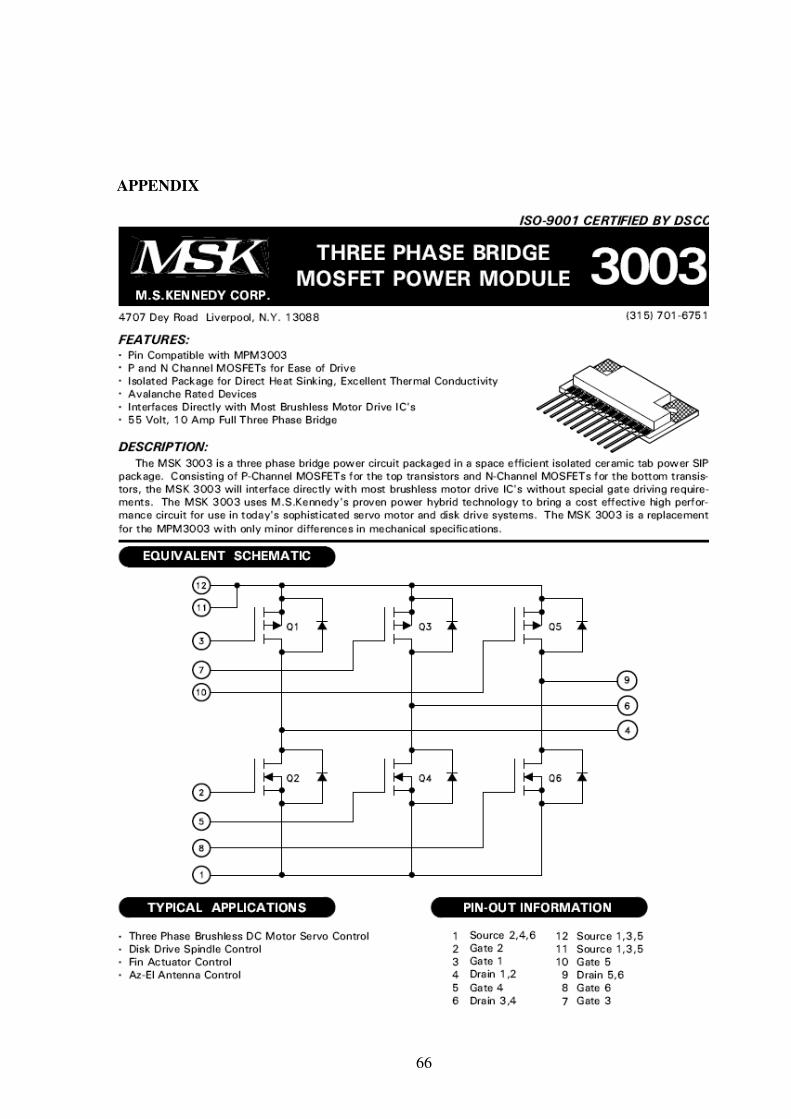
66
APPENDIX

67

68

69

70