Manufacturing Process of Silicon Wafer
12
Silicon Wafer
-
Upload
wafer-world-inc -
Category
Business
-
view
143 -
download
4
Transcript of Manufacturing Process of Silicon Wafer
Manufacturing Process of
Silicon Wafer
SiliconSilicon is a chemical
element that makes up
almost 30% of the earth’s
crust.
Silicon is the most
common material to build
semiconductors and
microchips with despite
the fact that on its own, it
doesn’t conduct electricity
very well.
75%
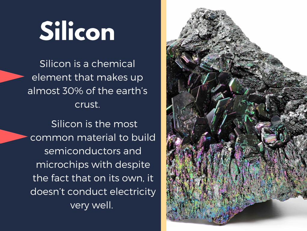
Ingot GrowthGrowing a silicon
ingot can range in
time from one week
to one month
depending on factors
such as size, quality,
and specification.
The adding of
dopants gives the
electrical properties
needed to grow
ingot.
of silicon wafers
grow via the
Czochralski (CZ)
method,.
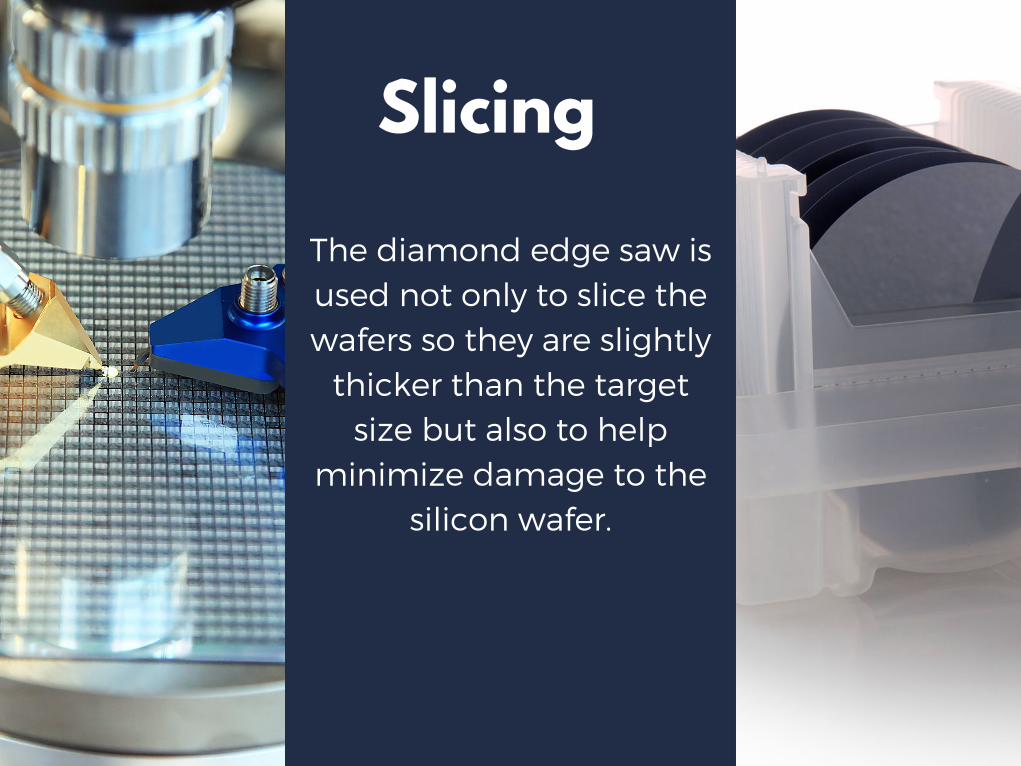
Slicing
The diamond edge saw is
used not only to slice the
wafers so they are slightly
thicker than the target
size but also to help
minimize damage to the
silicon wafer.
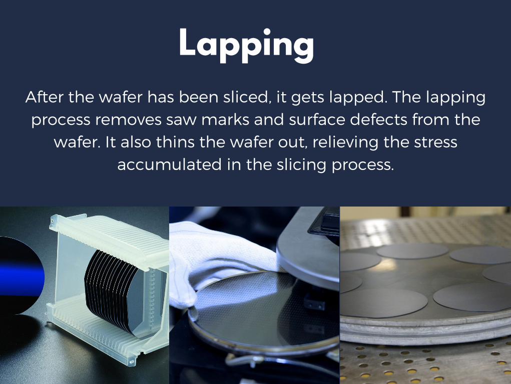
LappingAfter the wafer has been sliced, it gets lapped. The lapping
process removes saw marks and surface defects from the
wafer. It also thins the wafer out, relieving the stress
accumulated in the slicing process.
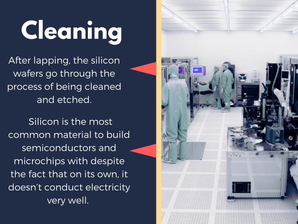
CleaningAfter lapping, the silicon
wafers go through the
process of being cleaned
and etched.
Silicon is the most
common material to build
semiconductors and
microchips with despite
the fact that on its own, it
doesn’t conduct electricity
very well.

Polishing
The polishing process
takes place in a clean
room where the workers
wear cleanroom suits
that cover their entire
bodies.

Are you looking for the silicon wafer in West Palm Beach?
Welcomes you
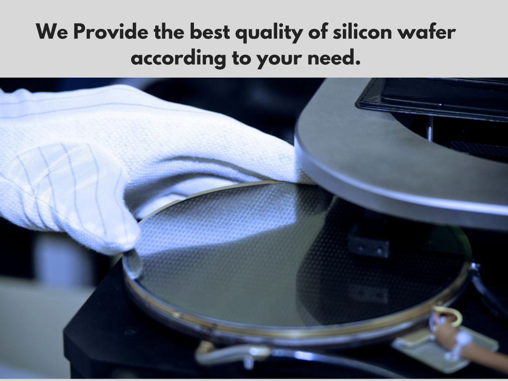
We Provide the best quality of silicon wafer according to your need.
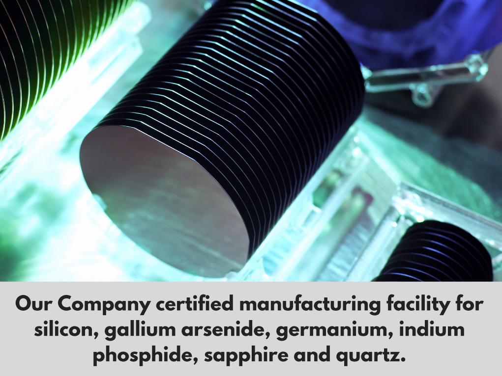
Our Company certified manufacturing facility for silicon, gallium arsenide, germanium, indium
phosphide, sapphire and quartz.

For our services
www.waferworld.com(561) 842-4441


![Ultra-Precision Step Stage for Silicon Wafer Scannersscholarships.engin.umich.edu/wp-content/uploads/sites/36/...manufacturing equipment such as wafer scanners [1, 2]. The demand of](https://static.fdocuments.in/doc/165x107/609e6b0be6da415d6858b659/ultra-precision-step-stage-for-silicon-wafer-manufacturing-equipment-such-as.jpg)
