FROM SILICA TO SILICON WAFER
43
Silicon V2.1 En FROM SILICA TO SILICON WAFER The Silicon Single Crystal and Wafers Manufacturing Version 2.1 En
description
FROM SILICA TO SILICON WAFER. The Silicon Single Crystal and Wafers Manufacturing Version 2.1 En. This presentation was prepared for the needs of the company ON Semiconductor with the aim to approximate the production principles of single crystal silicon ingots and silicon wafers. - PowerPoint PPT Presentation
Transcript of FROM SILICA TO SILICON WAFER
Silicon V2.1 En
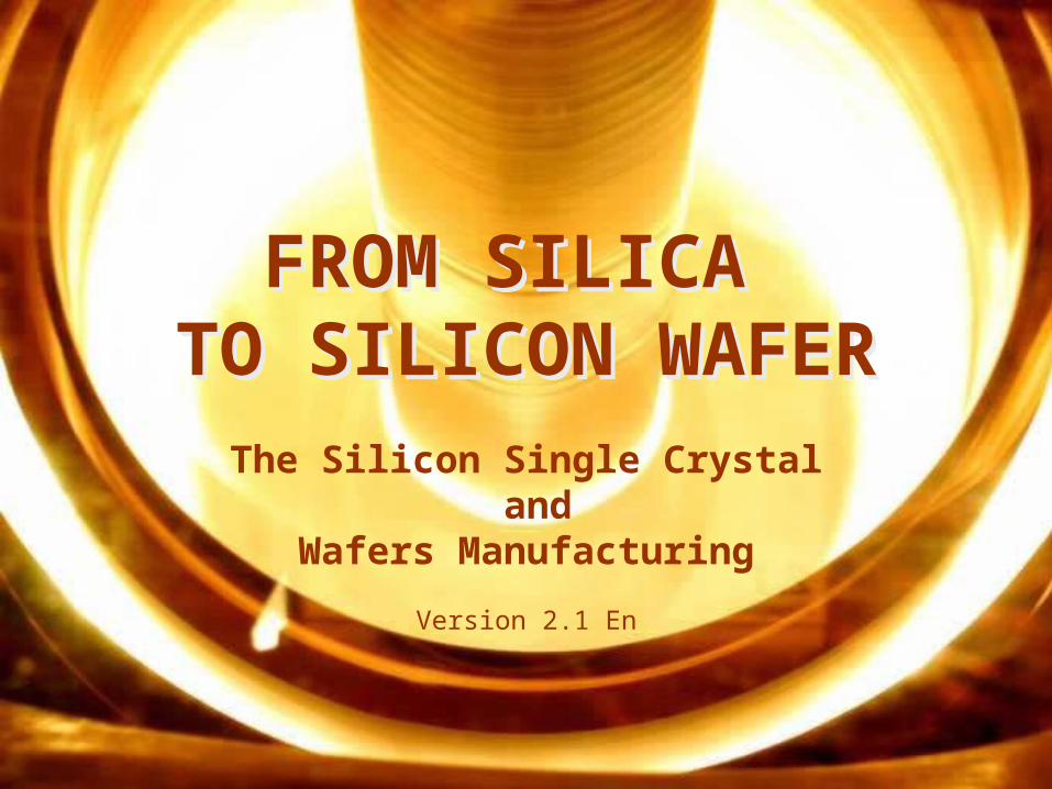
FROM SILICA TO SILICON WAFER
FROM SILICA TO SILICON WAFER
The Silicon Single Crystal and
Wafers Manufacturing
Version 2.1 En
2Silicon V2.1 En
VPS
VPS s.r.o., P.O. Box B-11, Partizanska 31, 921 01 Piestany 1, Slovak Republic
tel., fax.: +421 33 7730151, email: [email protected]
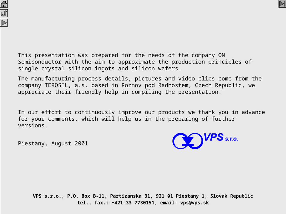
This presentation was prepared for the needs of the company ON Semiconductor with the aim to approximate the production principles of single crystal silicon ingots and silicon wafers.
The manufacturing process details, pictures and video clips come from the company TEROSIL, a.s. based in Roznov pod Radhostem, Czech Republic, we appreciate their friendly help in compiling the presentation.
In our effort to continuously improve our products we thank you in advance for your comments, which will help us in the preparing of further versions.
Piestany, August 2001
3Silicon V2.1 En
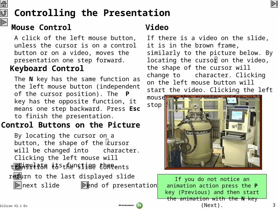
Controlling the Presentation
transition to the slide Contents
return to the last displayed slide
end of presentation
Control Buttons on the Picture
Mouse ControlA click of the left mouse button, unless the cursor is on a control button or on a video, moves the presentation one step forward.
Keyboard ControlThe N key has the same function as the left mouse button (independent of the cursor position). The P key has the opposite function, it means one step backward. Press Esc to finish the presentation.
Video
next slide
By locating the cursor on a button, the shape of the cursor will be changed into character. Clicking the left mouse will stimulate its function then.
If there is a video on the slide, it is in the brown frame, similarly to the picture below. By locating the cursor on the video, the shape of the cursor will change to character. Clicking on the left mouse button will start the video. Clicking the left mouse on the running video will stop it.
If you do not notice an animation action press the P key (Previous) and then start
the animation with the N key (Next).
Silicon V2.1 En 4
Appendix
Clean Rooms
Some Special Units
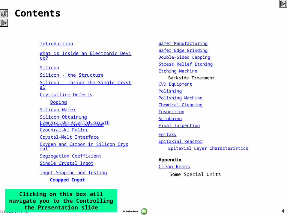
Contents
Introduction
What is Inside an Electronic Device?
Silicon
Silicon - the Structure
Silicon - Inside the Single Crystal
Crystalline Defects
Doping
Silicon Wafer
Silicon Obtaining
Polycrystalline Silicon
Clicking on this box will navigate you to the Controlling the Presentation
slide
Wafer Manufacturing
Wafer Edge Grinding
Double-Sided Lapping
Stress Relief Etching
Etching Machine
Backside Treatment
CVD Equipment
Polishing
Polishing Machine
Chemical Cleaning
Inspection
Scrubbing
Final Inspection
Epitaxy
Epitaxial Reactor
Epitaxial Layer Characteristics
Czochralski Crystal Growth
Czochralski Puller
Crystal-Melt Interface
Oxygen and Carbon in Silicon Crystal
Segregation Coefficient
Single Crystal Ingot
Ingot Shaping and Testing
Cropped Ingot
5Silicon V2.1 En
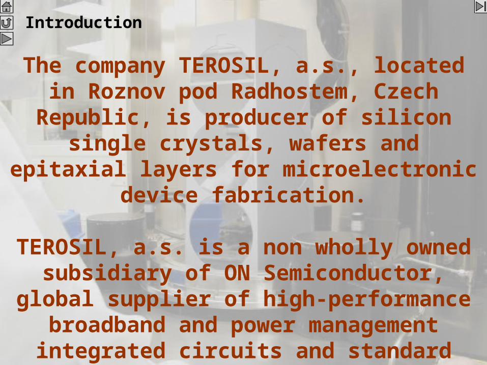
Introduction
The company TEROSIL, a.s., located in Roznov pod Radhostem, Czech Republic, is
producer of silicon single crystals, wafers and epitaxial layers for microelectronic device
fabrication.
TEROSIL, a.s. is a non wholly owned subsidiary of ON Semiconductor, global
supplier of high-performance broadband and power management integrated circuits and
standard semiconductors.
6Silicon V2.1 En
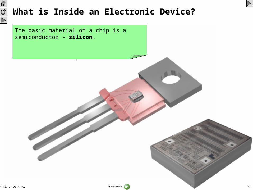
What is Inside an Electronic Device?
If we remove the black material from the package, we can see the leads leading up to a small piece of matter inside which the whole function of an electronic device proceeds.
This small piece of matter is called chip. After an enlargement we can see its structure.The basic material of a chip is a semiconductor - silicon.
7Silicon V2.1 En
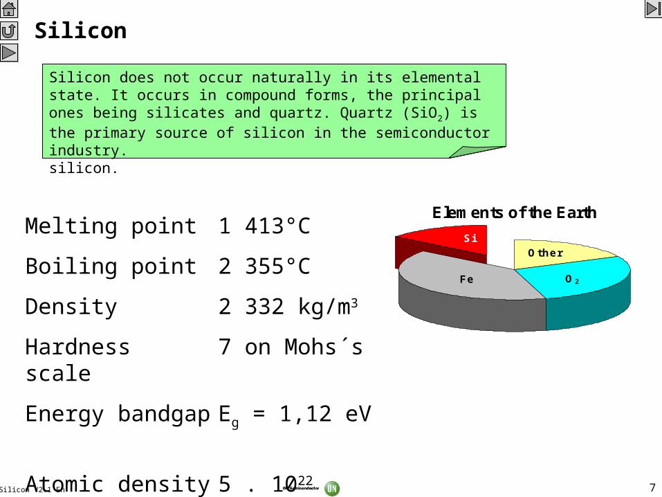
Silicon
Silicon is available in great abundance on the Earth. The Earth is made up of approximately 40% iron (Fe), 28% oxygen (O2) and 14,5% silicon. In the Earth´s crust, silicon is even the second most abundant element - the crust contains 28% of silicon.
Silicon does not occur naturally in its elemental state. It occurs in compound forms, the principal ones being silicates and quartz. Quartz (SiO2) is the primary source of silicon in the semiconductor industry.
Elements of the Earth
Si
Fe O2
Other
Melting point 1 413°C
Boiling point 2 355°C
Density 2 332 kg/m3
Hardness 7 on Mohs´s scale
Energy bandgap Eg = 1,12 eV
Atomic density 5 . 1022 atom/cm3
8Silicon V2.1 En
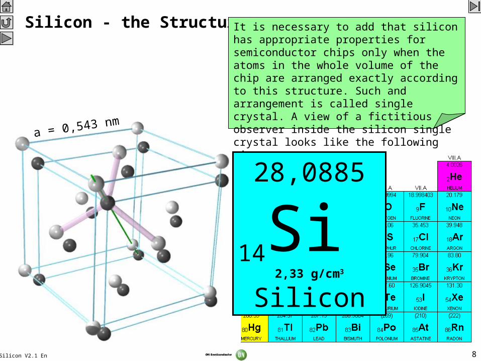
Silicon - the Structure
a = 0,543 nm
Silicon is a chemical element from the group IV in the Periodic table.Silicon crystallographic structure is diamond type lattice. It is based on a face centered cubic structure - a cube with atoms in its vertices and in the wall centers.
If we move a copy of this structure by 1/4 of the main diagonal, both the original and the shifted atoms form a diamond type lattice.
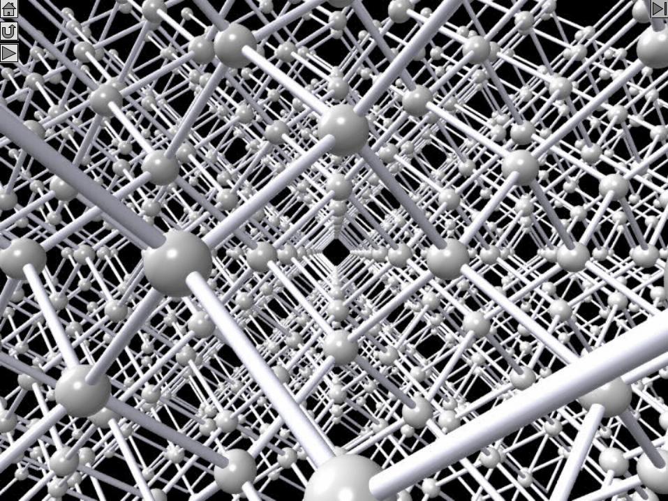
Each silicon atom has four neighbors, which it forms a bond with.It is necessary to add that silicon has appropriate properties for semiconductor chips only when the atoms in the whole volume of the chip are arranged exactly according to this structure. Such and arrangement is called single crystal. A view of a fictitious observer inside the silicon single crystal looks like the following picture.
28,0885
14Si 2,33 g/cm3
Silicon
9Silicon V2.1 En
Silicon - Inside the Single Crystal
10Silicon V2.1 En
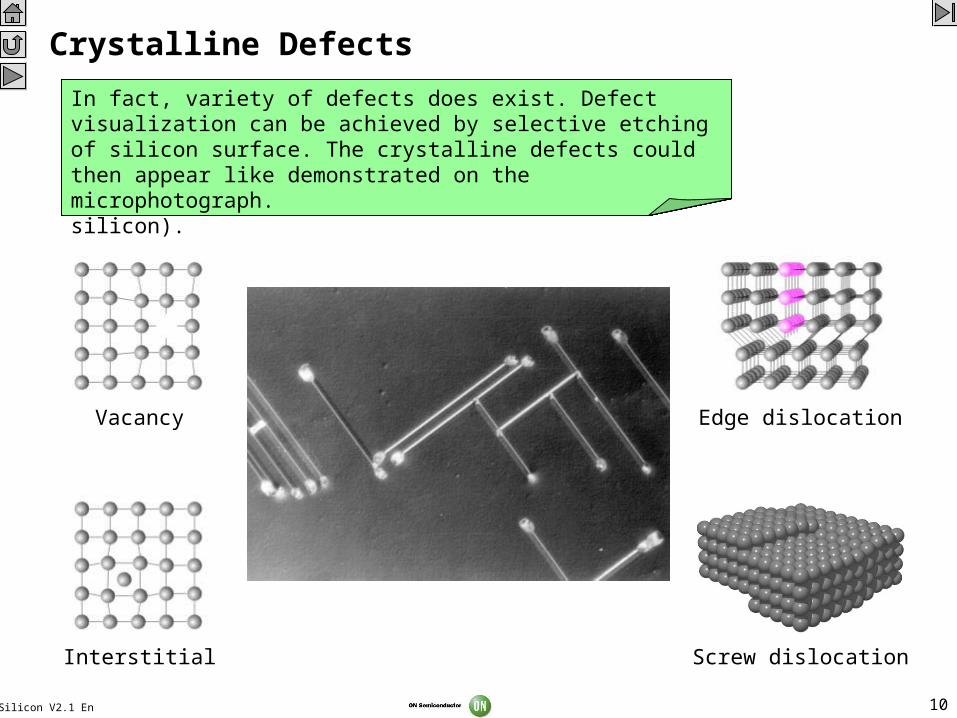
Crystalline Defects
Any imperfection in the crystalline structure is considered a defect. A defect can influence the electrical and mechanical properties of a crystal. To demonstrate various kinds of crystalline defects a simplified crystalline structure is used (not silicon).
An atom missing from the regular crystal site gives rise to a vacancy.
Vacancy
Interstitial
Edge dislocation
Screw dislocation
An additional atom occupying a site inbetween regular sites is called an intersticial.An edge dislocation appears as if an extra plane has been inserted into the crystal.A screw dislocation can be described as atomic layers partly cut with scissors and shifted each other.In fact, variety of defects does exist. Defect visualization can be achieved by selective etching of silicon surface. The crystalline defects could then appear like demonstrated on the microphotograph.
11Silicon V2.1 En
III.A V.AIV.A
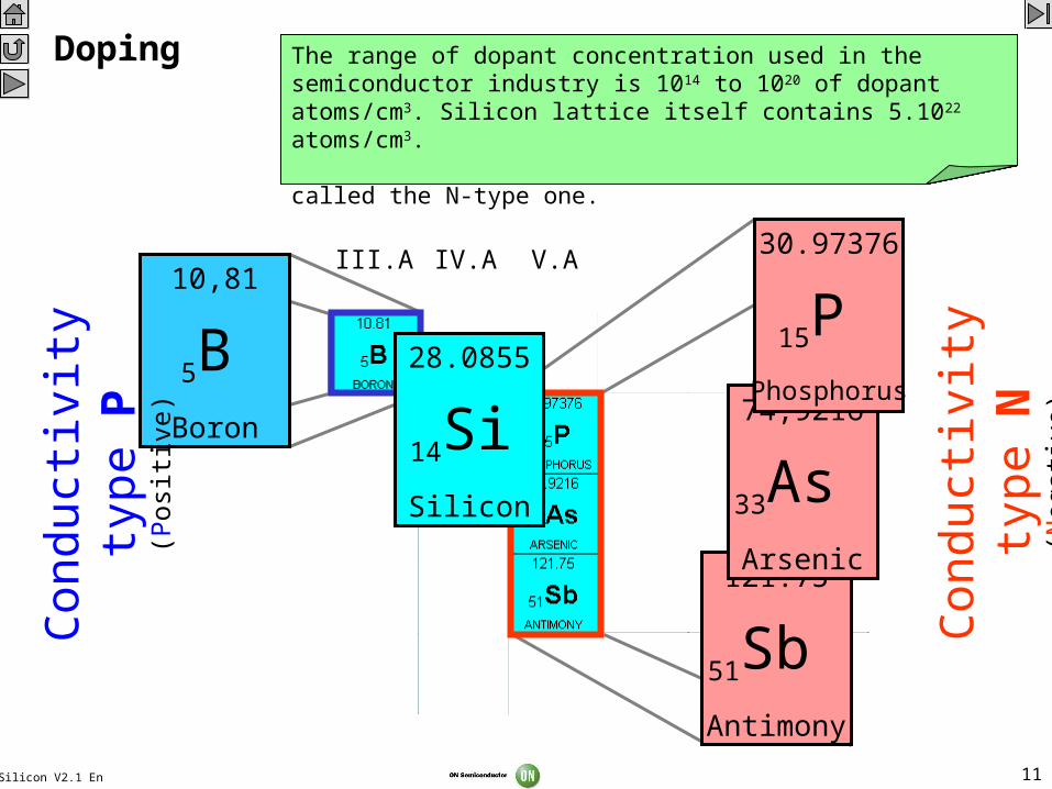
Doping Presence of some chemical elements - dopants in silicon, can substantially influence the silicon electric conductivity. Boron, phosphorus, arsenic and antimony are especially used for this purpose.
Physically, boron presence causes a different mechanism of electric current transfer in silicon than phosphorus or arsenic. Silicon doped with boron is called the P-type silicon while silicon doped with phosphorus, arsenic or antimony is called the N-type one.
Only a very small amount of a dopant is sufficient for doping silicon. The unit of a dopant concentration is the number of dopant atoms per unit volume of silicon, usually given in #atoms/cm3.
The range of dopant concentration used in the semiconductor industry is 1014 to 1020 of dopant atoms/cm3. Silicon lattice itself contains 5.1022 atoms/cm3.
121.75
51Sb Antimony
74,9216
33As Arsenic
30.97376
15P
Phosphorus
10,81
5B
Boron
28.0855
14Si Silicon
Con
duct
ivity
type
P(P
ositi
ve)
Con
duct
ivity
type
N(N
egat
ive)
12Silicon V2.1 En
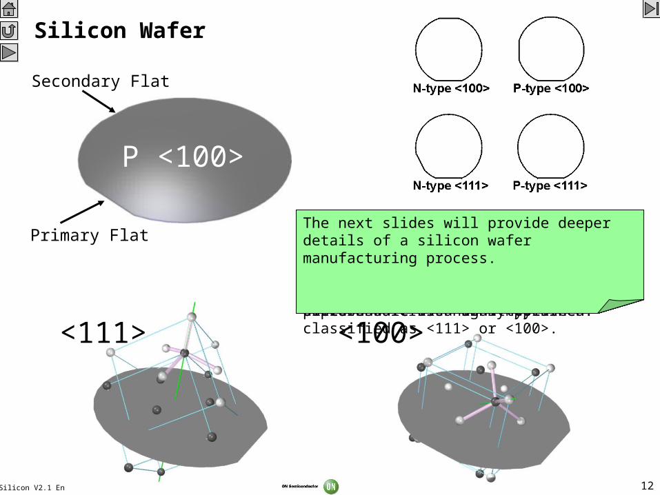
Silicon Wafer
A chip is very small, just a few square millimeters. It would be difficult, if not even impossible, to produce each chip individually.
Primary Flat
Secondary Flat
<100><111>
For that reason, many chips are processed together in one slice of semiconductor - silicon wafer. At the end of the process the wafer is cut up into individual chips.
The silicon wafer is round-shaped. The diameters of 100, 125, 150 mm or more are commonly used. A 100 mm wafer is about half of millimeter thick. Already the wafer material is doped and it is P or N-type then.
The crystallographic orientation, in respect to the silicon wafer surface, is important for the wafer properties. In practice, the orientations according to the pictures are used and they are classified as <111> or <100>.
The conductivity (P or N) type and a silicon wafer crystallographic orientation are encoded in a relative position of primary and secondary flat on each wafer. The top side of silicon wafer is highly polished.
The wafers are fabricated by cutting from a monocrystalline silicon cylinder pulled from molten silicon in special equipment.
P <100>
The next slides will provide deeper details of a silicon wafer manufacturing process.
13Silicon V2.1 En
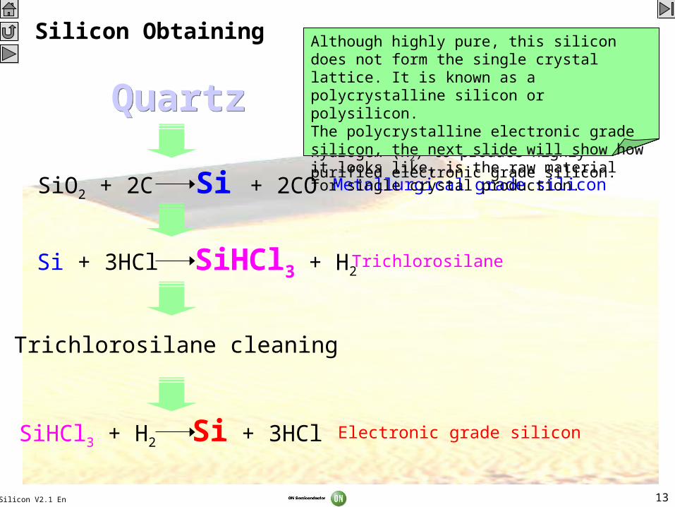
At the very first step the quartz sand is transformed into the silicon. This silicon, known as metallurgical grade silicon, is obtained by chemical reaction of quartz with carbon (C).
Silicon Obtaining
SiO2 + 2C Si + 2CO
Si + 3HCl SiHCl3 + H2
SiHCl3 + H2 Si + 3HCl
Metallurgical grade silicon
Electronic grade silicon
Trichlorosilane
Trichlorosilane cleaning
QuartzQuartz
Metallurgical grade silicon is not pure enough for semiconductor technology. Thus it is converted to trichlorsilane (SiHCl3), which can be cleaned by distillation, and then this trichlorsilane is reacted with hydrogen (H2) to produce highly purified electronic grade silicon.
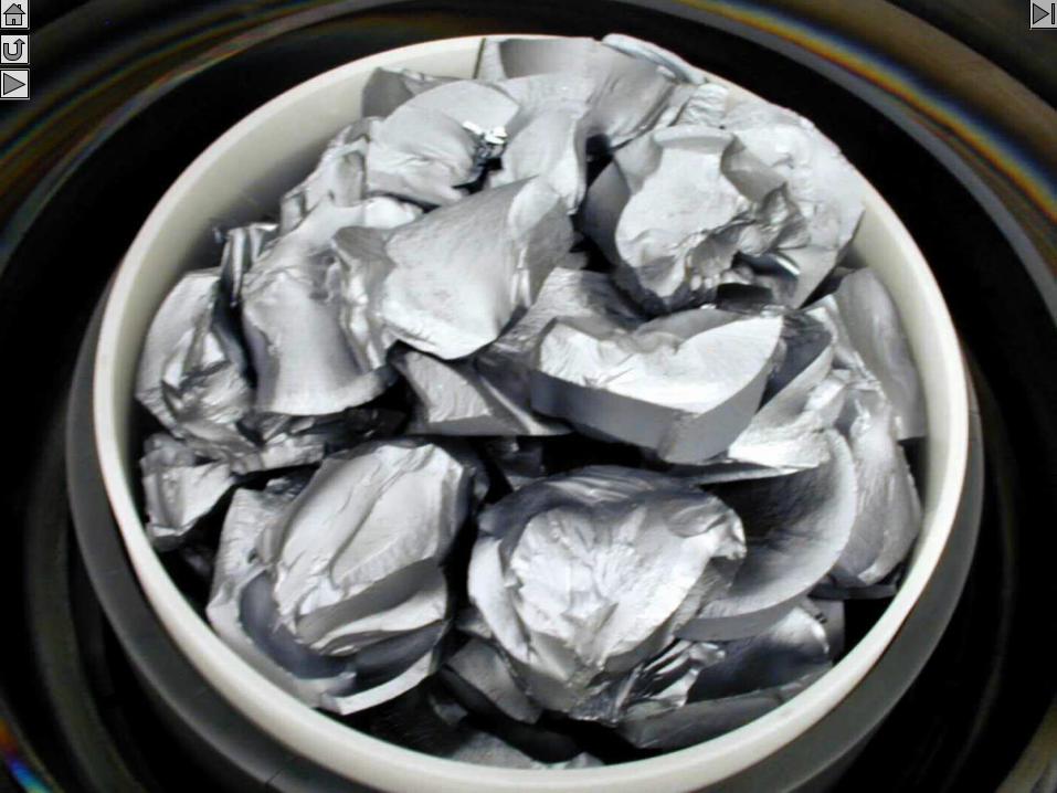
Although highly pure, this silicon does not form the single crystal lattice. It is known as a polycrystalline silicon or polysilicon.The polycrystalline electronic grade silicon, the next slide will show how it looks like, is the raw material for single crystal production.
Silicon V2.1 En 14
Polycristalline Silicon
Silicon V2.1 En 15
Appendix
Clean Rooms
Some Special Units
Chapter 1 Overview
Introduction
What is Inside an Electronic Device?
Silicon
Silicon - the Structure
Silicon - Inside the Single Crystal
Crystalline Defects
Doping
Silicon Wafer
Silicon Obtaining
Polycrystalline Silicon
Wafer Manufacturing
Wafer Edge Grinding
Double-Sided Lapping
Stress Relief Etching
Etching Machine
Backside Treatment
CVD Equipment
Polishing
Polishing Machine
Chemical Cleaning
Inspection
Scrubbing
Final Inspection
Epitaxy
Epitaxial Reactor
Epitaxial Layer Characteristics
Czochralski Crystal Growth
Czochralski Puller
Crystal-Melt Interface
Oxygen and Carbon in Silicon Crystal
Segregation Coefficient
Single Crystal Ingot
Ingot Shaping and Testing
Cropped Ingot
16Silicon V2.1 En
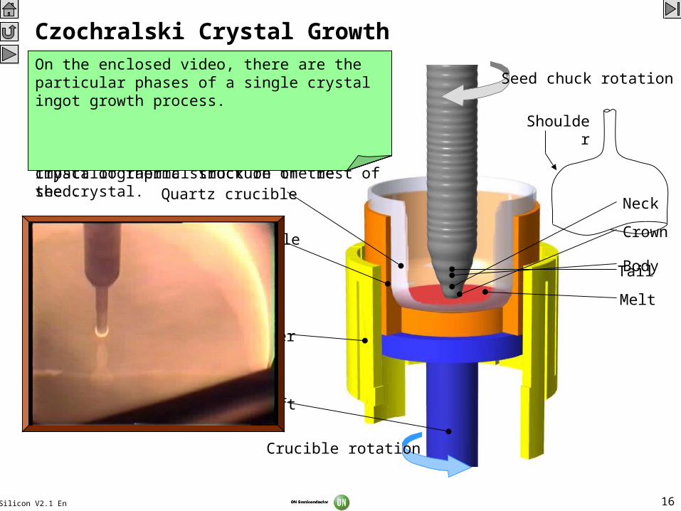
Czochralski Crystal Growth
Seedchuck
Seed
Crucible rotation
Seed chuck rotation
Quartz crucible
Graphite crucible(susceptor)
Graphite heater
Crucible shaft
Melt
Neck
Crown
BodyTail
Shoulder
In 1918, Czochralski described a process in which a single crystal is pulled from a melt. Since then this method has been significally refined and remain the most popular method to produce high quality single crystals.
The goal is to transform raw materials into a silicon single crystal. The quartz crucible is loaded with the polysilicon (see photo) and the dopant. A seed crystal is also loaded in the puller.
The crystallographic orientation of the seed will be adapted by growing crystal. It has to be chosen in accordance to the final silicon wafer orientation required.
The polysilicon charge is melted in the quartz crucible. The crystal seed is then dipped into the silicon melt. The seed is rotated and simultaneously pulled-up from the melt. A crystal grows at the interface following the crystallographic structure of the seed.
In this initial phase, the pull rate is high to maintain a small diameter for the growing crystal. This procedure is called necking and its purpose is to eliminate dislocations from the crystal.
The pull rate is then decreased and the diameter of the crystal is increased to the desired size. This second part of the initial growth is called crowning.
Reachnig the desired diameter a "shoulder" is formed on the growing crystal shape.The crystal is progressively grown and pulled out of the melt. The critical process parameters that must be controlled are the temperatures, the pull rate, the rotation rates and low pressure argon ambient.
Both the growing crystal and the crucible rotate as indicated by arrows. The melt is consumed, therefore the crucible lifts to keep melt level at the same height.
In the final phase, the pull speed is increased to reduce the crystal diameter. When the crystal body is removed from the melt a quick temperature change is induced. A thin "tail" on the crystal end reduces the impact of thermal shock on the rest of the crystal.
On the enclosed video, there are the particular phases of a single crystal ingot growth process.
17Silicon V2.1 En
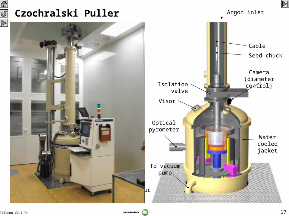
Czochralski Puller
Quartz crucible
Graphite crucible
Graphite heater
Thermal shield
Electric current lead-in
Crucible shaft
Crucible rotation
Seed chuckrotation
Cable
Seed chuck
The quartz crucible is the component containing the silicon melt. The crucible material must be chosen such that it reacts very slowly with the melt. The only material that can be used is quartz.
Argon inlet
Opticalpyrometer
Camera(diameter control)
Isolation valve
Visor
To vacuumpump
Watercooled jacket
The quartz crucible is supported by a graphite crucible which serves simultaneously as the heat susceptor. Both crucibles are placed on a graphite shaft enabling the rotation and lifting.
A graphite heating element is placed around the graphite crucible - susceptor. Finally, the last part of the heat zone is a thermal shield eliminating the heat losses.The lift (seed chuck and cable) holds the seed and growing crystal during the process enabling the controlled pull rate and rotation.
The whole system is placed in vacuum chamber with water-cooled jacket. Monitoring system (pyrometer and camera) and computer control the growth process.
An isolation valve allows access to upper chamber while keeping the controled ambient in lower vacuum chamber.
The Czochralski puller schematical drawing can be compared with real equipment picture next.
18Silicon V2.1 En
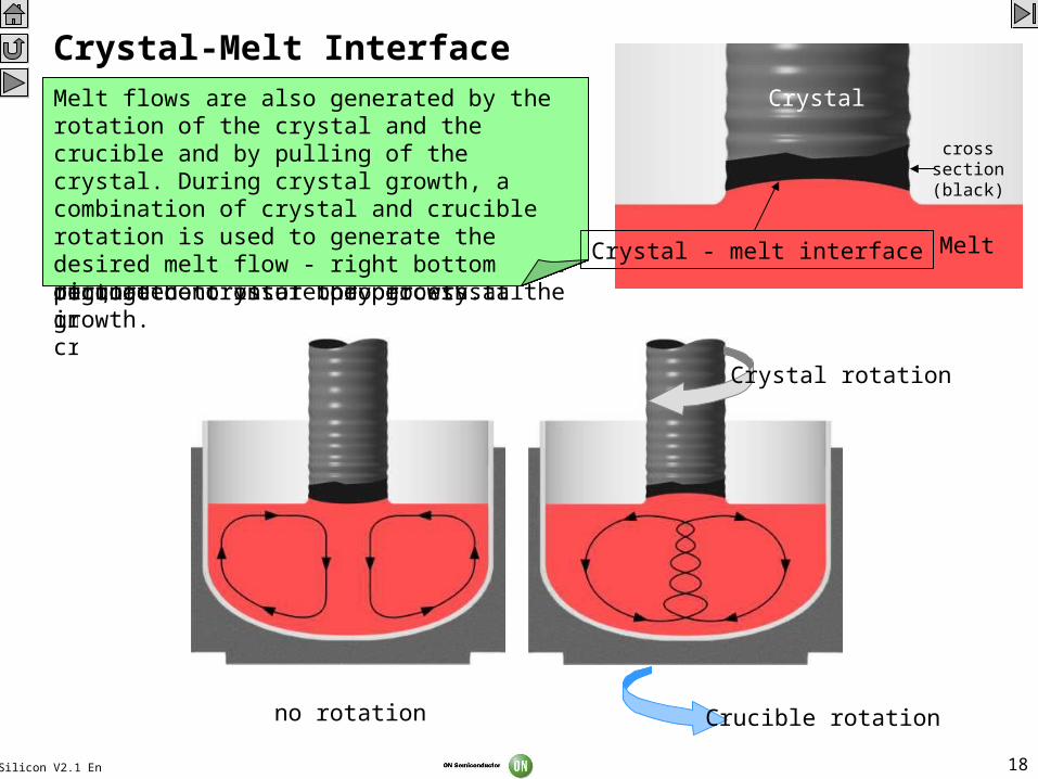
Crystal-Melt InterfaceThe fundamental process behind the growth of a crystal involves the transformation of a liquid into a solid. To grow a crystal, the atoms of the liquid must organize themselves as they become part of the solid. This underlines the importance of good control of the process at the interface between the melt and the crystal.
Hea
t flo
w
Heat input Heat output
Melt flow Melt flow
Convex crystal-melt interface Concave crystal-melt interface
A good control of the temperature at the interface between the crystal and the melt is crucial. A good control of the heat flow throughout the interface is the critical condition for that.
The area between the melt and crystal has to be maintained at the silicon freezing point. This is the coldest region in the melt, otherwise solidification will occur in other parts as well. Heat inputs and outputs must be monitored and be regulated to insure proper crystal growth.
The crystallization takes place at the crystal-melt interface. The shape of the interface directly influences the crystalline perfection and the impurity distribution throughout the section. The concave shape helps to remove dislocations and is maintained during the crystal body growth.
During crystal growth, the melt flow pattern in the crucible plays an important role of crystal-melt interface shape and dopant variation. The spontaneous melt flow originates from temperature differences in the melt - left bottom picture.
Melt flows are also generated by the rotation of the crystal and the crucible and by pulling of the crystal. During crystal growth, a combination of crystal and crucible rotation is used to generate the desired melt flow - right bottom picture.
Crystal rotation
Crucible rotationno rotation
Crystal - melt interface Melt
Crystal
cross section(black)
19Silicon V2.1 En
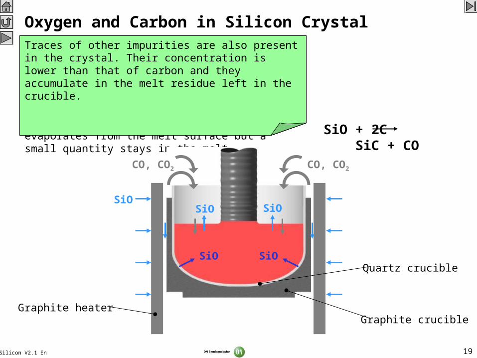
Oxygen and Carbon in Silicon CrystalOxygen is the most common impurity in silicon crystal. Its main source is the crucible material - quartz (SiO2). This surface is in contact with the silicon melt. The reaction between the silicon melt and the crucible produces silicon monoxide (SiO). Most of the silicon monoxide evaporates from the melt surface but a small quantity stays in the melt.
Quartz crucible
Graphite heaterGraphite crucible
Carbon impurities originate from the polysilicon charge and from the reaction between the graphite heating element and silicon monoxide evaporated from the melt. Carbon has much lower concentration than oxygen in the crystal.
Traces of other impurities are also present in the crystal. Their concentration is lower than that of carbon and they accumulate in the melt residue left in the crucible.
CO, CO2 CO, CO2
SiO SiO
SiO SiOSiO
SiO + 2C SiC + CO
20Silicon V2.1 En
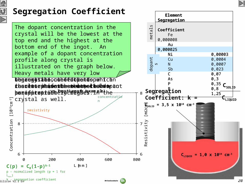
Dopant Concentration/Resistivityvs. Ingot Length (example)
6
8
10
0 200 400 600 800
L [mm]
6
7
8concentration
Co
nce
ntr
atio
n [
1019
cm-3]
C(p) = C0(1-p)k-1
p - normalized length (p = 1 for Lmax)k - segregation coefficient
Re
sist
ivity
[m
cm
]
resistivity
CLIQUID = 1,0 x 1019 cm-3
CSOLID = 3,5 x 1018 cm-3
Segregation Coefficient: k =CSOLID
CLIQUID
One of the key operations in crystal pulling is the introduction of a specific amount of dopant into the crystal. The dopant is added to the polysilicon charge or melt in the crucible.
Segregation Coefficient
In the crystal growth process, there are two phases at the interface - the solid crystal and the liquid melt. Between the two phases, redistribution of the dopant takes place. This is measured in term of a segregation coefficient as a ratio of concentrations of the dopant in the two phases.
For example, phosphorus has a segregation coefficient of 0,35. That is, near the interface, dopant concentration in the crystal will be 0,35 times the concentration of phosphorus in the melt. Therefore, in order to achieve a given dopant level in the crystal, the dopant concentration in the melt has to be appropriately higher.
Most of elements have segregation coefficient less than unity. Due to this, only a part of dopant is integrated into the crystal. The rest is rejected back into the melt. It results in dopant accumulation in the melt as crystal growth proceeds. In turn, because the concentration increases in the melt, the dopant concentration increases in the crystal as well.
The dopant concentration in the crystal will be the lowest at the top end and the highest at the bottom end of the ingot. An example of a dopant concentration profile along crystal is illustrated on the graph below. Heavy metals have very low segregation coefficients which results in further material purification.
Element Segregation Coefficient
Fe 0,000008Au 0,000025Ni 0,00003Cu 0,0004N 0,0007Sb 0,023C 0,07As 0,3P 0,35B 0,8O 1,25
Element Segregation Coefficient
Fe 0,000008Au 0,000025Ni 0,00003Cu 0,0004N 0,0007Sb 0,023C 0,07As 0,3P 0,35B 0,8O 1,25
me
tals
do
pa
nts
Silicon V2.1 En 21
Single Crystal Ingot
Silicon V2.1 En 22
Appendix
Clean Rooms
Some Special Units
Chapter 2 Overview
Introduction
What is Inside an Electronic Device?
Silicon
Silicon - the Structure
Silicon - Inside the Single Crystal
Crystalline Defects
Doping
Silicon Wafer
Silicon Obtaining
Polycrystalline Silicon
Wafer Manufacturing
Wafer Edge Grinding
Double-Sided Lapping
Stress Relief Etching
Etching Machine
Backside Treatment
CVD Equipment
Polishing
Polishing Machine
Chemical Cleaning
Inspection
Scrubbing
Final Inspection
Epitaxy
Epitaxial Reactor
Epitaxial Layer Characteristics
Czochralski Crystal Growth
Czochralski Puller
Crystal-Melt Interface
Oxygen and Carbon in Silicon Crystal
Segregation Coefficient
Single Crystal Ingot
Ingot Shaping and Testing
Cropped Ingot
23Silicon V2.1 En
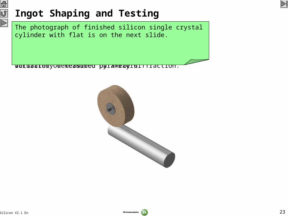
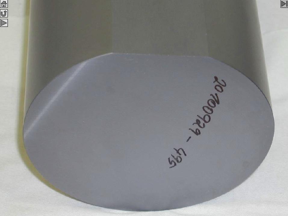
Ingot Shaping and TestingThe pulled ingot is cut into individual sections. This operation is called cropping. Each section is examided for defects. Also, the ends of the ingot are removed.
X-ray source
Detector
During the cropping of the crystal, a few thin slices are removed for testing. Usually resistivity profiles, oxygen and carbon concentration and crystallographic defects are tested. The set of slices allows to verify the variation of measured parameters.
The crystal section is placed in the grinding machine and the machine grinds down the crystal until the target diameter of the cylinder is reached.
Crystallographic orientation of the cylinder axis is given by the seed orientation. To identify a radial crystallographic orientation of the crystal a flat is ground into it. Knowing the orientation, the position of the flat is accurately determined by X-ray diffraction.
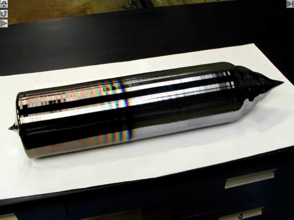
The photograph of finished silicon single crystal cylinder with flat is on the next slide.
Silicon V2.1 En 24
Cropped Ingot
Silicon V2.1 En 25
Appendix
Clean Rooms
Some Special Units
Chapter 3 Overview
Introduction
What is Inside an Electronic Device?
Silicon
Silicon - the Structure
Silicon - Inside the Single Crystal
Crystalline Defects
Doping
Silicon Wafer
Silicon Obtaining
Polycrystalline Silicon
Wafer Manufacturing
Wafer Edge Grinding
Double-Sided Lapping
Stress Relief Etching
Etching Machine
Backside Treatment
CVD Equipment
Polishing
Polishing Machine
Chemical Cleaning
Inspection
Scrubbing
Final Inspection
Epitaxy
Epitaxial Reactor
Epitaxial Layer Characteristics
Czochralski Crystal Growth
Czochralski Puller
Crystal-Melt Interface
Oxygen and Carbon in Silicon Crystal
Segregation Coefficient
Single Crystal Ingot
Ingot Shaping and Testing
Cropped Ingot

26Silicon V2.1 En
Wafer ManufacturingThe first step in the production of silicon wafers from a crystal ingot is sawing. A graphite beam is attached to the crystal with an adhesive to hold the wafer after the saw blade has cut through the ingot.
VIDEO 352 x 288
Stainless steel core
Nickel matrix with imbedded diamond
particles
Silicon
Damage
Water
The saw is made of a thin stainless steel with a hole in the center. A nickel matrix with imbedded diamond particles is plated around the inner edge of the blade. This diamond-nickel matrix provides a surface which is used to cut the silicon ingot.
When cutting wafers from a crystal, it is desired to make a flat cut at a specific angle with respect to the crystal orientation and to waste as little material as possible with a minimum of damage of the wafers. For that the blade is cooled and rinsed by water with surfactant.
The damage comes from the fact that sawing process is really a form of grinding. The damage exists wherever the blade comes in contact with the crystal. Therefore, the damaged material has to be removed in the subsequent steps. On the enclosed video, there is a shot of sawing process.
27Silicon V2.1 En
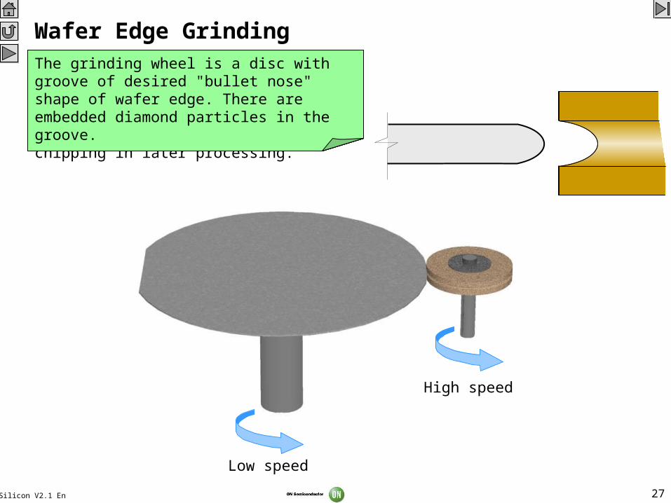
Wafer Edge GrindingAfter sawing, the wafers have an edge with sharp corners. The edge is ground to form a bullet shaped edge. This increases edge strength and make the edges less prone to chipping in later processing.
Low speed
High speed
The wafer is placed on vacuum chuck and slowly turned as the grinding wheel, which is rotating at high speed, is forced against the wafer edge.
The grinding wheel is a disc with groove of desired "bullet nose" shape of wafer edge. There are embedded diamond particles in the groove.
28Silicon V2.1 En
Double-Sided Lapping
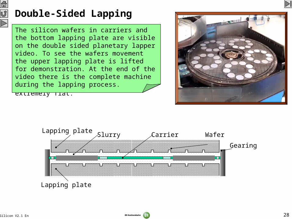
The next step in wafer production is called lapping. Purpose of this step is to make wafer surface smooth, flat and parallel.
During lapping, wafers are placed in a carrier and are driven between two cast iron made lapping plates. The carrier is thinner than the wafers allowing both sides of the wafer to be lapped simultaneously.
An abrasive slurry (aluminium oxide Al2O3 suspended in water with surfactant) is fed to the wafers surface as they are moved between the lapping plates. This removes the silicon and leaves behind a more uniform surface. Wafers are very flat because the lapping plates are extremely flat.
The silicon wafers in carriers and the bottom lapping plate are visible on the double sided planetary lapper video. To see the wafers movement the upper lapping plate is lifted for demonstration. At the end of the video there is the complete machine during the lapping process.
VIDEO 352 x 288
CarrierLapping plate
Lapping plate
Wafer
Gearing
Slurry
29Silicon V2.1 En
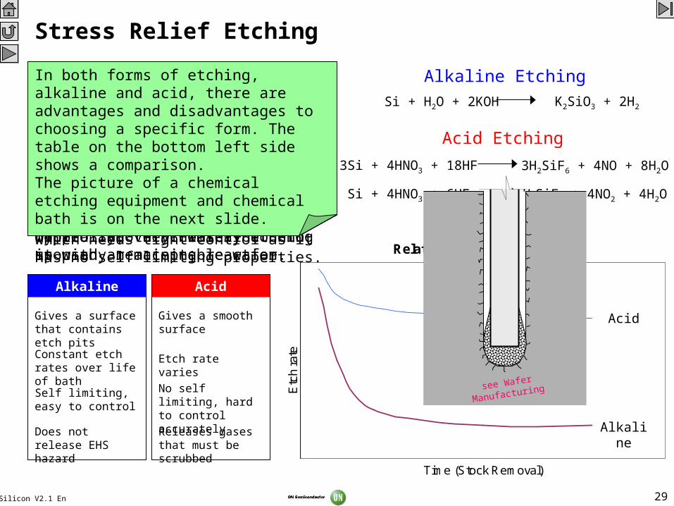
Relative etching rates vs. time
Time (Stock Removal)
Etc
h ra
te
Acid
Alkaline
Stress Relief Etching
Since lapping allows only to remove the bulk of the saw damage and always leaves a thin uniform layer of damage, some other method must be used to remove the damage from lapping. This damage needs to be removed while causing as little additional damage as possible. Typically, the chemical etching is used.
One method of etching the wafers is the use of an alkaline hydroxide, such as potassium hydroxide (KOH). In this method, the wafers are dipped in KOH and water mixture for about 2 minutes. The mixture is usually at elevated temperature of about 100°C. Then the wafers are dipped into a DI water bath to stop any remaining reaction.
Another form of etching used on silicon wafers is acid etching. A common mixture used for acid etching is HNO3 and HF. Sometimes, additional chemicals are added to the mixture to make the reaction more controllable. In any case, the acid etching process is a vigorous process which needs tight control as it has no self limiting properties.
The figure below shows a relative comparison of the etch rates of a typical acid and a typical alkaline etch. It can be seen that the acid etch continues to etch silicon wafer at a high rate for as long as the two are kept in contact. Therefore the acid etch must be controlled very closely to end up with an acceptable wafer.
In both forms of etching, alkaline and acid, there are advantages and disadvantages to choosing a specific form. The table on the bottom left side shows a comparison.The picture of a chemical etching equipment and chemical bath is on the next slide.
Si + H2O + 2KOH K2SiO3 + 2H2
Alkaline Etching
Acid Etching
3Si + 4HNO3 + 18HF 3H2SiF6 + 4NO + 8H2O
Si + 4HNO3 + 6HF H2SiF6 + 4NO2 + 4H2O
Alkaline
Gives a surface that contains etch pits
Constant etch rates over life of bath
Self limiting, easy to control
Does not release EHS hazard
Acid
Gives a smooth surface
Etch rate varies
No self limiting, hard to control accurately
Releases gases that must be scrubbed
see Wafer Manufacturing
30Silicon V2.1 En
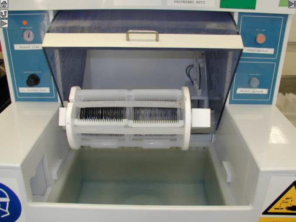
Etching Machine
31Silicon V2.1 En
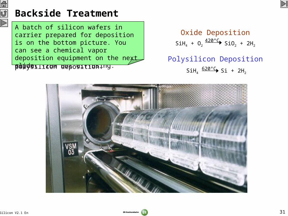
Backside TreatmentFor wafers that are highly doped and are going to go through a high temperature process, a layer is deposited on the back side of the wafer to prevent the dopant from out diffusing.
Silicon dioxide can be used as a backseal. The layer is deposited on the wafer by chemical vapor deposition. The oxide acts strictly as a sealant.
Polysilicon on the backside prevents out diffusing as well as getters heavy metals from the bulk of the wafer. Normally a silane (SiH4) source is used for polysilicon deposition.
A batch of silicon wafers in carrier prepared for deposition is on the bottom picture. You can see a chemical vapor deposition equipment on the next slide.
Oxide Deposition
SiH4 + O2 SiO2 + 2H2
420°C
Polysilicon Deposition
SiH4 Si + 2H2620°C
32Silicon V2.1 En
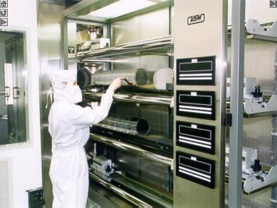
CVD Equipment
33Silicon V2.1 En
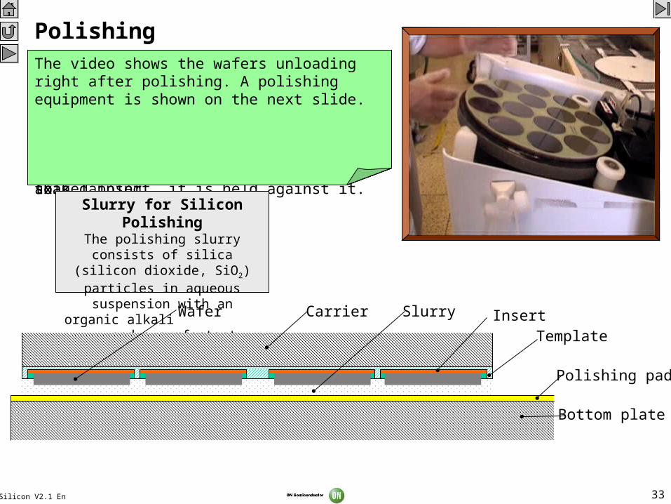
Slurry
PolishingThe purpose of wafer polishing is to produce a very smooth, flat, damage free silicon surface. The polishing step is, unlike lapping, a chemical/mechanical process. This difference is the reason polishing produces a much smoother final surface than lapping.
One of the polishing techniques is the template mounting method. The wafers are situated in a round template attached on a carrier and set on a soft polyurethane insert in the template. The insert has a porous structure. When the wafer is pressed against the water soaked insert, it is held against it.
A polishing pad is mounted on the bottom plate. The soft insert is necessary to hold the wafers in place when the wafers are mounted to the polishing equipment with the surface facing down. The bottom plate and carriers are rotating around their own axis.
The video shows the wafers unloading right after polishing. A polishing equipment is shown on the next slide.
Slurry for Silicon PolishingThe polishing slurry consists of
silica (silicon dioxide, SiO2) particles in aqueous suspension with an organic alkali
and a surfactant.
Bottom plate
Polishing pad
Wafer InsertCarrier
Template
34Silicon V2.1 En
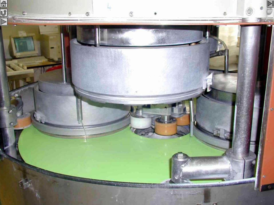
Polishing Machine
35Silicon V2.1 En
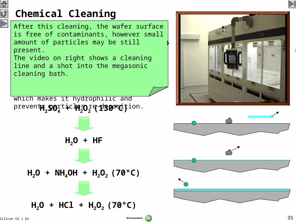
Chemical CleaningAfter the wafers have been polished, they have a large number of contaminants on the surface. In general, these contaminants are particles, organic residuals and metallic ions. The chemical cleaning is designed to remove them.
H2SO4 + H2O2 (130°C)
H2O + HF
H2O + NH4OH + H2O2 (70°C)
H2O + HCl + H2O2 (70°C)
The most common method of cleaning the wafers after polishing is a wet cleaning consisting of several chemical steps. The first one is a hot mixture of sulfuric acid and hydrogen peroxide called Piranha. It decomposes virtually any organics on the wafer surface into carbon dioxide and water.
At the time of chemical cleaning, the wafers have a thin native oxide layer on top and the contaminants are mostly on top of the oxide or embedded within it. The role of the subsequent step, diluted hydrofluoric acid, is to etch out the native oxide and polishing slurry residuals.
The most commonly used method to remove particles is the SC1 (Standard Clean 1) solution. This mixture is the hot NH4OH and H2O2 in water. Ammonium hydroxide under-etches particles attached to the surface and eliminates attractive forces. Hydrogen peroxide is oxidizing agent to grow thin clean oxide layer on the wafer surface, which makes it hydrophilic and prevents particles re-deposition.
After previous steps some metals may still remain on the wafer surface. The cleaning agent for the metal contaminants is a mixture of HCl and H2O2 in water. This mixture is known as SC2 (Standard Clean 2). The mixture oxidizes and reacts with metals on the silicon surface and removes them.
The chemical cleaning operation is complemented by megasonic cleaning. Megasonic waves are acoustic waves of very high frequency (about 1 MHz). The waves exert forces on particles on wafer surface and help to detach them.
After this cleaning, the wafer surface is free of contaminants, however small amount of particles may be still present.The video on right shows a cleaning line and a shot into the megasonic cleaning bath.
Organic residual
Particle
Native SiO2
Metallic ion
VIDEO 352 x 288
36Silicon V2.1 En
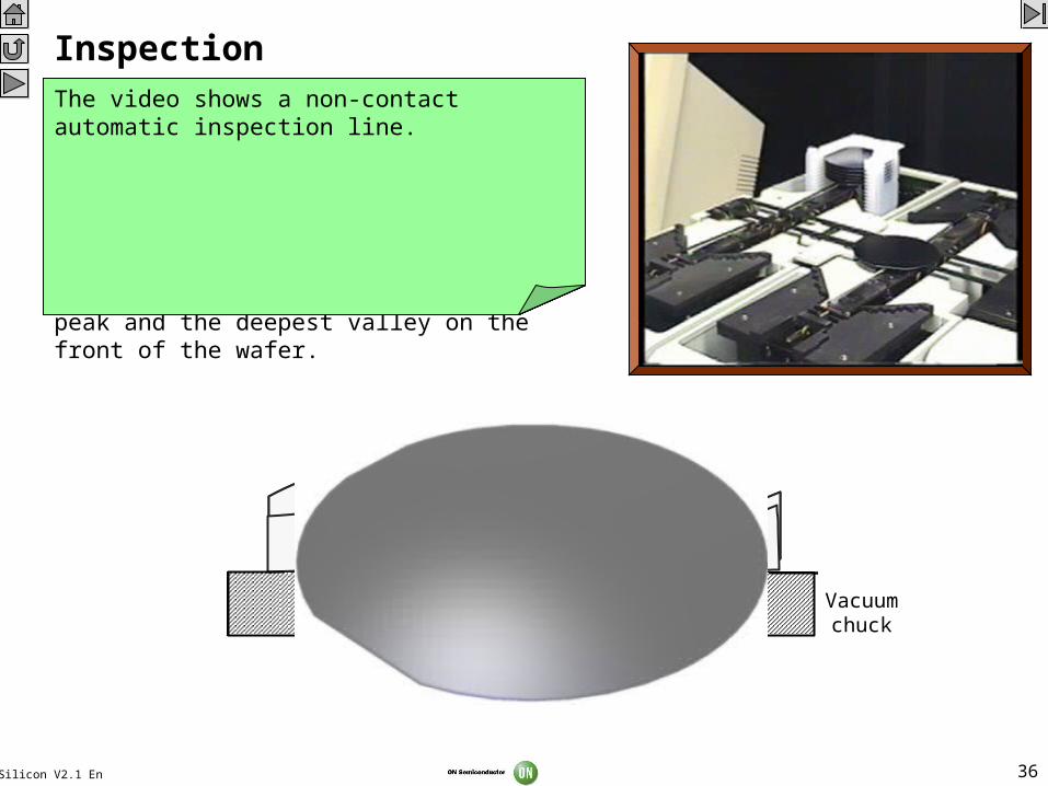
InspectionAfter the wafers have been polished and cleaned, they are ready to be inspected. During the inspection process, the resistivity and geometrical parameters are measured by non-contact methods. VIDEO 352 x 288
A measure of the shape deformation of a wafer is warp. Warp is the measure of maximum difference between the highest and lowest location of the centerline of a wafer with respect to reference plane defined by three pedestals near the wafer edge.
A measurement of the consistency of a wafer thickness is total thickness variation (TTV). It is the difference between the maximum and minimum thickness of a wafer.
The total indicator reading (TIR) is a measurement that is only concerned with the front side of a wafer. The way this measurement is made is by reference to a plane that is parallel to the vacuum chuck that the wafer is mounted on. The TIR is the difference between the height of the highest peak and the deepest valley on the front of the wafer.
The video shows a non-contact automatic inspection line.
Wafer centerline
Referenceplane
Dmax
Wafer
Dmin
Warp = (Dmax - Dmin) / 2
Tmax
Wafer
Tmin
TTV = Tmax - TminTIR = hmax - hmin
hmax
Wafer
hmin
Vacuumchuck
37Silicon V2.1 En
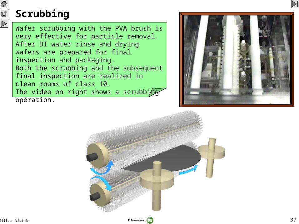
VIDEO 352 x 288
The wafers are cleaned to remove particles and metal contamination but after inspection may have an increased number of particles on the surface again. The scrubbing has to be used for final mechanical/chemical cleaning.
During the scrubbing aqueous ammonium hydroxide (NH4OH) flows across the wafer surface to remove the particles. Simultaneously the brushing is made by polyvinil alcohol (PVA) fibers which do not scratch the wafer when brought into direct contact with the wafer surface.
Wafer scrubbing with the PVA brush is very effective for particle removal. After DI water rinse and drying wafers are prepared for final inspection and packaging.Both the scrubbing and the subsequent final inspection are realized in clean rooms of class 10.The video on right shows a scrubbing operation.
Scrubbing
Silicon V2.1 En 38
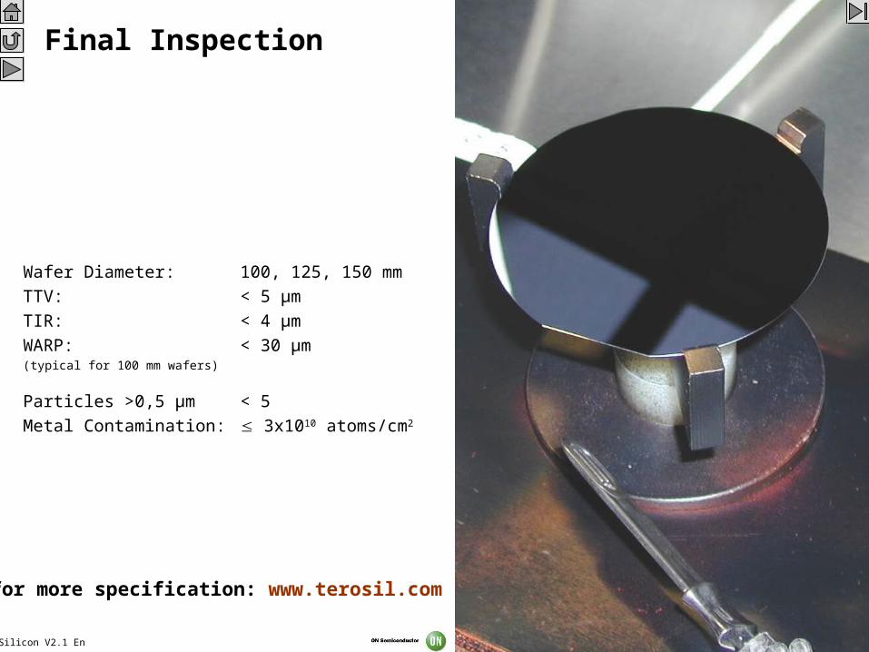
Wafer Diameter: 100, 125, 150 mm
TTV: < 5 µm
TIR: < 4 µm
WARP: < 30 µm(typical for 100 mm wafers)
Particles >0,5 µm < 5
Metal Contamination: 3x10¹⁰ atoms/cm2
Final Inspection
for more specification: www.terosil.com
Silicon V2.1 En 39
Appendix
Clean Rooms
Some Special Units
Chapter 4 Overview
Introduction
What is Inside an Electronic Device?
Silicon
Silicon - the Structure
Silicon - Inside the Single Crystal
Crystalline Defects
Doping
Silicon Wafer
Silicon Obtaining
Polycrystalline Silicon
Wafer Manufacturing
Wafer Edge Grinding
Double-Sided Lapping
Stress Relief Etching
Etching Machine
Backside Treatment
CVD Equipment
Polishing
Polishing Machine
Chemical Cleaning
Inspection
Scrubbing
Final Inspection
Epitaxy
Epitaxial Reactor
Epitaxial Layer Characteristics
Czochralski Crystal Growth
Czochralski Puller
Crystal-Melt Interface
Oxygen and Carbon in Silicon Crystal
Segregation Coefficient
Single Crystal Ingot
Ingot Shaping and Testing
Cropped Ingot
40Silicon V2.1 En
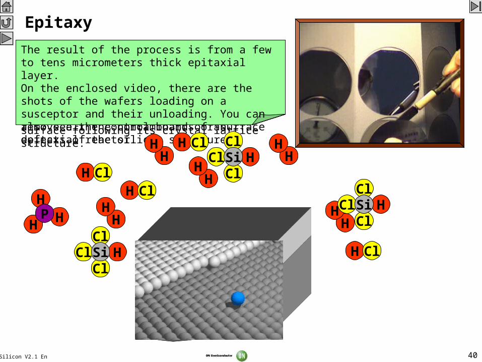
For particular applications there is a need to form a layer of high resistivity material on top of lower resistivity material. The epitaxial growth is used for this purpose.
Epitaxy is the growth of the silicon layer on the silicon wafer surface. The layer has the same crystallographic properties as the substrate, but it can have a different dopant concentration or even different dopant.
Epitaxy
VIDEO 320 x 240
P
HHH
PSi
Si Si
SiSi
The process proceeds at high temperature about 1200 °C. Hydrogen flows past the incandescent silicon wafers. When hydrogen chloride is added, it starts reacting with silicon and it etches the wafer surface away. It is important to remove all the contaminants or surface defects of the silicon structure.
After the surface etching is finished, the silicon chloride (SiHCl3) vapors are introduced. SiHCl3 reacts with present hydrogen at a high temperature. The result of this reaction are free silicon atoms that settle on the silicon wafer surface following its crystal lattice structure.
If there are any phosphine (PH3) molecules present, the phosphorus atoms dope the growing epitaxial layer. Boron compounds can be used for doping as well.
HH
HH
HH
HH
HH
H Cl
H Cl
H Cl
H Cl
The result of the process is from a few to tens micrometers thick epitaxial layer.On the enclosed video, there are the shots of the wafers loading on a susceptor and their unloading. You can also see the control board of an epitaxial reactor.
Cl HCl
ClSi
Cl HCl
ClSi
Cl HCl
ClSi
41Silicon V2.1 En
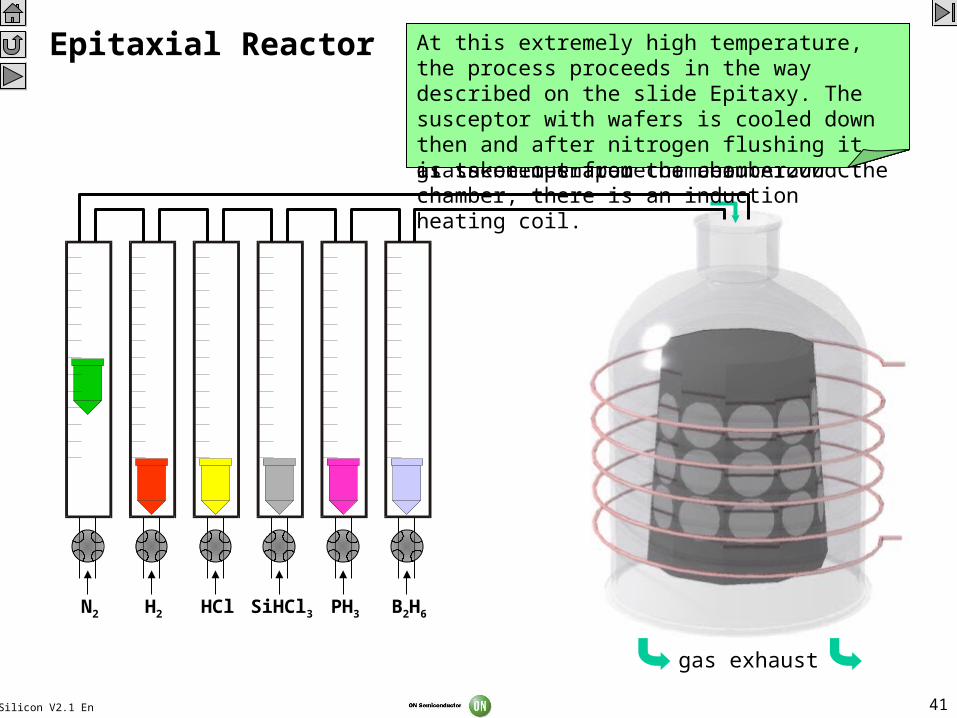
Epitaxial Reactor
N2 H2 HCl SiHCl3 PH3 B2H6
Epitaxial reactor is an equipment for the growth of the epitaxial layer. Silicon wafers are loaded on a graphite block - susceptor. The susceptor is placed inside a quartz glass bell-shaped chamber. Around the chamber, there is an induction heating coil.
gas exhaust
During the process, the chamber with the wafers is flushed with nitrogen and hydrogen. In the hydrogen environment the susceptor with wafers is warmed up by the induction heating at the temperature of about 1200°C.
At this extremely high temperature, the process proceeds in the way described on the slide Epitaxy. The susceptor with wafers is cooled down then and after nitrogen flushing it is taken out from the chamber.
Silicon V2.1 En 42
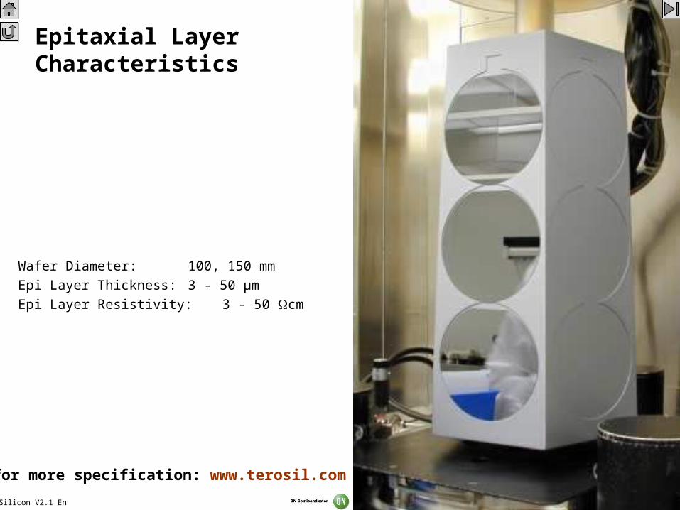
Epitaxial LayerCharacteristics
Wafer Diameter: 100, 150 mm
Epi Layer Thickness: 3 - 50 µm
Epi Layer Resistivity: 3 - 50 cm
for more specification: www.terosil.com
Silicon V2.1 En 43
Appendix
Clean Rooms
Some Special Units
Chapter 5 Overview
Introduction
What is Inside an Electronic Device?
Silicon
Silicon - the Structure
Silicon - Inside the Single Crystal
Crystalline Defects
Doping
Silicon Wafer
Silicon Obtaining
Polycrystalline Silicon
Wafer Manufacturing
Wafer Edge Grinding
Double-Sided Lapping
Stress Relief Etching
Etching Machine
Backside Treatment
CVD Equipment
Polishing
Polishing Machine
Chemical Cleaning
Inspection
Scrubbing
Final Inspection
Epitaxy
Epitaxial Reactor
Epitaxial Layer Characteristics
Czochralski Crystal Growth
Czochralski Puller
Crystal-Melt Interface
Oxygen and Carbon in Silicon Crystal
Segregation Coefficient
Single Crystal Ingot
Ingot Shaping and Testing
Cropped Ingot