LTC4364-1/LTC4364-2 - Surge Stopper with Ideal … 4 436412f ELECTRICAL CHARACTERISTICS The l...
24
LTC4364-1/LTC4364-2 1 436412f TYPICAL APPLICATION FEATURES DESCRIPTION Surge Stopper with Ideal Diode The LTC ® 4364 surge stopper with ideal diode controller protects loads from high voltage transients. It limits and regulates the output during an overvoltage event, such as load dump in automobiles, by controlling the voltage drop across an external N-channel MOSFET pass device. The LTC4364 also includes a timed, current limited circuit breaker. In a fault condition, an adjustable fault timer must expire before the pass device is turned off. The LTC4364-1 latches off the pass device while the LTC4364-2 automati- cally restarts after a delay. The LTC4364 precisely monitors the input supply for overvoltage (OV) and undervoltage (UV) conditions. The external MOSFET is held off in un- dervoltage and auto-retry is disabled in overvoltage. An integrated ideal diode controller drives a second MOS- FET to replace a Schottky diode for reverse input protec- tion and output voltage holdup. The LTC4364 controls the forward voltage drop across the MOSFET and minimizes reverse current transients upon power source failure, brownout or input short. Overvoltage Protector Regulates Output at 27V During Input Transient Ideal Diode Holds Up Output During Input Short 4A, 12V Overvoltage Output Regulator with Ideal Diode Withstands 200V 1ms Transient at V IN APPLICATIONS n Wide Operating Voltage Range: 4V to 80V n Withstands Surges Over 80V with V CC Clamp n Adjustable Output Clamp Voltage n Ideal Diode Controller Holds Up Output Voltage During Input Brownouts n Reverse Input Protection to –40V n Reverse Output Protection to –20V n Overcurrent Protection n Low 10μA Shutdown Current at 12V n Adjustable Fault Timer n 0.1% Retry Duty Cycle During Faults (LTC4364-2) n Available in 4mm × 3mm 14-Lead DFN, 16-Lead MSOP , and 16-Lead SO Packages n Automotive/Avionic Surge Protection n Hot Swap/Live Insertion n Redundant Supply ORing n Output Port Protection L, LT, LTC, LTM, Linear Technology and the Linear logo are registered trademarks of Linear Technology Corporation. All other trademarks are the property of their respective owners. + OUT SENSE DGATE SOURCE HGATE TMR GND 0.22μF UV UV 6V OV 60V OV ENOUT ENABLE FAULT 436412 TA01a FLT SHDN FB 10Ω 2.2k 383k V IN 12V 90.9k 10k 102k 22μF V OUT CLAMPED AT 27V 4.99k CMZ5945B 68V FDB33N25 FDB3682 10mΩ 6.8nF V CC LTC4364 50ms/DIV C TMR = 6.8μF I LOAD = 0.5A V IN 20V/DIV 12V 12V V OUT 20V/DIV 92V INPUT SURGE 27V CLAMP (ADJUSTABLE) 4364 TA01b 1ms/DIV C LOAD = 6300μF I LOAD = 0.5A V IN 10V/DIV 12V 12V V OUT 10V/DIV 4364 TA01c INPUT SHORTED TO GND OUTPUT HELD UP
Transcript of LTC4364-1/LTC4364-2 - Surge Stopper with Ideal … 4 436412f ELECTRICAL CHARACTERISTICS The l...

LTC4364-1/LTC4364-2
1436412f
TYPICAL APPLICATION
FEATURES DESCRIPTION
Surge Stopper with Ideal Diode
The LTC®4364 surge stopper with ideal diode controller protects loads from high voltage transients. It limits and regulates the output during an overvoltage event, such as load dump in automobiles, by controlling the voltage drop across an external N-channel MOSFET pass device. The LTC4364 also includes a timed, current limited circuit breaker. In a fault condition, an adjustable fault timer must expire before the pass device is turned off. The LTC4364-1 latches off the pass device while the LTC4364-2 automati-cally restarts after a delay. The LTC4364 precisely monitors the input supply for overvoltage (OV) and undervoltage (UV) conditions. The external MOSFET is held off in un-dervoltage and auto-retry is disabled in overvoltage.
An integrated ideal diode controller drives a second MOS-FET to replace a Schottky diode for reverse input protec-tion and output voltage holdup. The LTC4364 controls the forward voltage drop across the MOSFET and minimizes reverse current transients upon power source failure, brownout or input short.
Overvoltage Protector RegulatesOutput at 27V During Input Transient
Ideal Diode Holds Up OutputDuring Input Short
4A, 12V Overvoltage Output Regulator with Ideal Diode Withstands 200V 1ms Transient at VIN
APPLICATIONS
n Wide Operating Voltage Range: 4V to 80Vn Withstands Surges Over 80V with VCC Clamp n Adjustable Output Clamp Voltagen Ideal Diode Controller Holds Up Output Voltage
During Input Brownoutsn Reverse Input Protection to –40Vn Reverse Output Protection to –20Vn Overcurrent Protectionn Low 10μA Shutdown Current at 12Vn Adjustable Fault Timern 0.1% Retry Duty Cycle During Faults (LTC4364-2)n Available in 4mm × 3mm 14-Lead DFN, 16-Lead MSOP,
and 16-Lead SO Packages
n Automotive/Avionic Surge Protectionn Hot Swap/Live Insertionn Redundant Supply ORingn Output Port ProtectionL, LT, LTC, LTM, Linear Technology and the Linear logo are registered trademarks of Linear Technology Corporation. All other trademarks are the property of their respective owners.
+
OUTSENSEDGATESOURCEHGATE
TMRGND
0.22µF
UVUV6V
OV60V
OV ENOUT ENABLEFAULT
436412 TA01a
FLT
SHDN FB
10Ω2.2k
383k
VIN12V
90.9k
10k
102k
22µF
VOUTCLAMPEDAT 27V
4.99k
CMZ5945B68V
FDB33N25 FDB3682 10mΩ
6.8nF
VCC
LTC4364
50ms/DIV
CTMR = 6.8µFILOAD = 0.5A
VIN20V/DIV
12V
12VVOUT
20V/DIV
92V INPUT SURGE
27V CLAMP (ADJUSTABLE)
4364 TA01b
1ms/DIV
CLOAD = 6300µFILOAD = 0.5AVIN
10V/DIV
12V
12VVOUT10V/DIV
4364 TA01c
INPUT SHORTEDTO GND
OUTPUT HELD UP

LTC4364-1/LTC4364-2
2436412f
ABSOLUTE MAXIMUM RATINGSSupply Voltage: VCC ................................. –40V to 100VSOURCE, OV, UV, SHDN Voltages ............. –40V to 100VDGATE, HGATE Voltages (Note 3) ..................... SOURCE – 0.3V to SOURCE + 10VENOUT, FLT Voltages ................................ –0.3V to 100VOUT, SENSE Voltages.................................–20V to 100VVoltage Difference (SENSE to OUT) ............ –30V to 30VVoltage Difference (OUT to VCC) ..............–100V to 100VVoltage Difference (SENSE to SOURCE) ..–100V to 100V
(Notes 1, 2)
1
2
3
4
5
6
7
14
13
12
11
10
9
8
FB
TMR
ENOUT
FLT
GND
OV
UV
OUT
SENSE
DGATE
SOURCE
HGATE
VCC
SHDN
TOP VIEW
15
DE PACKAGE14-LEAD (4mm × 3mm) PLASTIC DFN
TJMAX = 150°C, θJA = 45°C/W EXPOSED PAD (PIN 15) PCB GND CONNECTION OPTIONAL
12345678
OUTSENSE
NCDGATE
SOURCEHGATE
NCVCC
161514131211109
FBTMRENOUTFLTGNDOVUVSHDN
TOP VIEW
MS PACKAGE16-LEAD PLASTIC MSOP
TJMAX = 150°C, θJA = 120°C/W
TOP VIEW
S PACKAGE16-LEAD PLASTIC SO
1
2
3
4
5
6
7
8
16
15
14
13
12
11
10
9
OUT
SENSE
NC
DGATE
SOURCE
HGATE
NC
VCC
FB
TMR
ENOUT
FLT
GND
OV
UV
SHDN
TJMAX = 150°C, θJA = 100°C/W
PIN CONFIGURATION
ORDER INFORMATIONLEAD FREE FINISH TAPE AND REEL PART MARKING* PACKAGE DESCRIPTION TEMPERATURE RANGE
LTC4364CDE-1#PBF LTC4364CDE-1#TRPBF 43641 14-Lead (4mm × 3mm) Plastic DFN 0°C to 70°C
LTC4364IDE-1#PBF LTC4364IDE-1#TRPBF 43641 14-Lead (4mm × 3mm) Plastic DFN –40°C to 85°C
LTC4364HDE-1#PBF LTC4364HDE-1#TRPBF 43641 14-Lead (4mm × 3mm) Plastic DFN –40°C to 125°C
LTC4364CDE-2#PBF LTC4364CDE-2#TRPBF 43642 14-Lead (4mm × 3mm) Plastic DFN 0°C to 70°C
LTC4364IDE-2#PBF LTC4364IDE-2#TRPBF 43642 14-Lead (4mm × 3mm) Plastic DFN –40°C to 85°C
LTC4364HDE-2#PBF LTC4364HDE-2#TRPBF 43642 14-Lead (4mm × 3mm) Plastic DFN –40°C to 125°C
LTC4364CMS-1#PBF LTC4364CMS-1#TRPBF 43641 16-Lead Plastic MSOP 0°C to 70°C
LTC4364IMS-1#PBF LTC4364IMS-1#TRPBF 43641 16-Lead Plastic MSOP –40°C to 85°C
LTC4364HMS-1#PBF LTC4364HMS-1#TRPBF 43641 16-Lead Plastic MSOP –40°C to 125°C
LTC4364CMS-2#PBF LTC4364CMS-2#TRPBF 43642 16-Lead Plastic MSOP 0°C to 70°C
LTC4364IMS-2#PBF LTC4364IMS-2#TRPBF 43642 16-Lead Plastic MSOP –40°C to 85°C
LTC4364HMS-2#PBF LTC4364HMS-2#TRPBF 43642 16-Lead Plastic MSOP –40°C to 125°C
FB, TMR Voltages ..................................... –0.3V to 5.5VOperating Ambient Temperature Range LTC4364C ................................................ 0°C to 70°C LTC4364I .............................................–40°C to 85°C LTC4364H .......................................... –40°C to 125°CStorage Temperature Range .................. –65°C to 150°CLead Temperature (Soldering, 10 sec) MS, SO Packages ............................................. 300°C

LTC4364-1/LTC4364-2
3436412f
ORDER INFORMATIONLEAD FREE FINISH TAPE AND REEL PART MARKING* PACKAGE DESCRIPTION TEMPERATURE RANGE
LTC4364CS-1#PBF LTC4364CS-1#TRPBF LTC4364S-1 16-Lead Plastic SO 0°C to 70°C
LTC4364IS-1#PBF LTC4364IS-1#TRPBF LTC4364S-1 16-Lead Plastic SO –40°C to 85°C
LTC4364HS-1#PBF LTC4364HS-1#TRPBF LTC4364S-1 16-Lead Plastic SO –40°C to 125°C
LTC4364CS-2#PBF LTC4364CS-2#TRPBF LTC4364S-2 16-Lead Plastic SO 0°C to 70°C
LTC4364IS-2#PBF LTC4364IS-2#TRPBF LTC4364S-2 16-Lead Plastic SO –40°C to 85°C
LTC4364HS-2#PBF LTC4364HS-2#TRPBF LTC4364S-2 16-Lead Plastic SO –40°C to 125°C
Consult LTC Marketing for parts specified with wider operating temperature ranges. *The temperature grade is identified by a label on the shipping container.Consult LTC Marketing for information on non-standard lead based finish parts.For more information on lead free part marking, go to: http://www.linear.com/leadfree/ For more information on tape and reel specifications, go to: http://www.linear.com/tapeandreel/
ELECTRICAL CHARACTERISTICS The l denotes the specifications which apply over the full operating temperature range, otherwise specifications are at TA = 25°C. VCC = 12V.
SYMBOL PARAMETER CONDITIONS MIN TYP MAX UNITS
VCC Operating Supply Range l 4 80 V
ICC Supply Current VCC = SOURCE = SENSE = OUT = 12V, No Fault l 370 750 µA
ICC(SHDN) Supply Current in Shutdown Shutdown l 10 50 μA
ICC(REV) Reverse Input Current VCC = −30V l 0 –10 μA
Surge Stopper
∆VHGATE HGATE Gate Drive, (VHGATE − VSOURCE) VCC = 4V, DGATE Low, IHGATE = 0µA, −1µA VCC = 8V to 80V, DGATE Low, IHGATE = 0µA, −1µA
l
l
5 10
7 12
9 16
V V
IHGATE(UP) HGATE Pull-Up Current VCC = HGATE = DGATE = SOURCE = 12V l –10 –20 –30 µA
IHGATE(DN) HGATE Pull-Down Current Overvoltage: FB = 1.5V, ∆VHGATE = 5V l 60 130 mA
Overcurrent: ∆VSNS = 100mV, ∆VHGATE = 5V l 60 130 mA
Shutdown/Fault Turn-Off: ∆VHGATE = 5V l 0.4 1 mA
ISRC SOURCE Input Current VCC = SOURCE = SENSE = OUT = 12V VCC = SOURCE = 12V, Shutdown VSOURCE = –30V
l
l
l
18 32
–2.0
40 90
–3.5
µA µA
mA
VFB FB Servo Voltage VCC = 12V to 80V l 1.22 1.25 1.28 V
IFB FB Input Current FB = 1.25V l 0 1 µA
∆VSNS Overcurrent Fault Threshold, (VSENSE – VOUT)
VCC = 4V to 80V, OUT = 2.5V to VCC, 0°C to 125°C VCC = 4V to 80V, OUT = 2.5V to VCC, –40°C to 125°C VCC = 4V to 80V, OUT = 0V to 1.5V
l
l
l
45 43 18
50 50 25
55 57 32
mV mV mV
ISNS SENSE Input Current SENSE = VCC = SOURCE = OUT = 12V SENSE = –15V
l
l
55 –2
110 –4
µA mA
ITMR(UP) TMR Pull-Up Current, Overvoltage TMR = 1V, FB = 1.5V, VCC – OUT = 0.5V TMR = 1V, FB = 1.5V, VCC – OUT = 75V
l
l
–1.3 –40
–2.2 –50
–3 –60
µA µA
TMR Pull-Up Current, Overcurrent TMR = 1V, ∆VSNS = 60mV, VCC – OUT = 0.5V TMR = 1V, ∆VSNS = 60mV, VCC – OUT = 75V
l
l
–6 –210
–10 –260
–14 –310
µA µA
TMR Pull-Up Current, Warning TMR = 1.3V, FB = 1.5V, VCC – OUT = 0.5V l –3 –5 –7 µA
TMR Pull-Up Current, Retry TMR = 1V, FB = 1.5V l –1.3 –2 –3 µA
ITMR(DN) TMR Pull-Down Current TMR = 1V, FB = 1.5V, Retry Shutdown
l
l
1.1 0.3
2 0.75
2.7 1.5
µA mA
VTMR(F) TMR Fault Threshold FLT Falling, VCC = 4V to 80V l 1.22 1.25 1.28 V
VTMR(G) TMR Gate Off Threshold HGATE Falling, VCC = 4V to 80V l 1.32 1.35 1.38 V

LTC4364-1/LTC4364-2
4436412f
ELECTRICAL CHARACTERISTICS The l denotes the specifications which apply over the full operating temperature range, otherwise specifications are at TA = 25°C. VCC = 12V.
SYMBOL PARAMETER CONDITIONS MIN TYP MAX UNITS
VTMR(R) TMR Retry Threshold HGATE Rising (After 32 Cycles), VCC = 4V to 80V l 0.125 0.15 0.175 V
∆VTMR Early Warning Timer Window VTMR(G) – VTMR(F), VCC = 4V to 80V l 75 100 125 mV
VUV UV Input Threshold UV Falling, VCC = 4V to 80V l 1.22 1.25 1.28 V
VUV(HYST) UV Input Hysteresis l 25 50 80 mV
VUV(RST) UV Reset Threshold UV Falling, VCC = 4V to 80V, LTC4364-1 Only l 0.5 0.6 0.7 V
VOV OV Input Threshold OV Rising, VCC = 4V to 80V l 1.22 1.25 1.28 V
VOV(HYST) OV Input Hysteresis 12 mV
IIN UV, OV Input Current UV, OV = 1.25V UV, OV = –30V
l
l
0 –0.3
1 –0.6
µA mA
VOL ENOUT, FLT Output Low ISINK = 0.25mA ISINK = 2mA
l
l
0.1 0.5
0.3 1.3
V V
ILEAK ENOUT, FLT Leakage Current ENOUT, FLT = 80V l 0 2.5 µA
∆VOUT(TH) Out High Threshold (VCC – VOUT) ENOUT from Low to High l 0.4 0.7 1 V
VOUT(RST) Out Reset Threshold ENOUT from High to Low l 1.4 2.2 3 V
IOUT OUT Input Current VCC = OUT = 12V, SHDN Open OUT = –15V
l
l
40 –4
80 –8
µA mA
Output Current in Shutdown, ISNS + IOUT VCC = SOURCE = SENSE = OUT = 12V, Shutdown l 12 40 µA
VSHDN SHDN Input Threshold VCC = 4V to 80V l 0.5 1.6 2.2 V
VSHDN(FLT) SHDN Pin Float Voltage VCC = 12V to 80V l 2.3 4 6.5 V
ISHDN SHDN Input Current SHDN = 0.5V Maximum Allowable Leakage, VCC = 4V SHDN = –30V
l
l
–1 –3.3 –1.5 –120
–300
µA µA µA
D Retry Duty Cycle, Overvoltage Retry Duty Cycle, Output Short
FB = 1.5V, VCC = 80V, OUT = 16V ∆VSNS = 60mV, VCC – OUT = 12V
l
l
0.125 0.075
0.2 0.12
% %
tOFF,HGATE(UV) Undervoltage to HGATE Low Propagation Delay
UV Steps from 1.5V to 1V l 1.3 4 μs
tOFF,HGATE(OV) Overvoltage to HGATE Low Propagation Delay
FB Steps from 1V to 1.5V l 0.25 1 μs
tOFF,HGATE(OC) Overcurrent to HGATE Low Propagation Delay
∆VSNS Steps from 0mV to 150mV, OUT = 0V l 0.5 2 μs
Ideal Diode
ΔVDGATE DGATE Gate Drive, (VDGATE − VSOURCE) VCC = 4V, No Fault, IDGATE = 0µA, −1µA VCC = 8V to 80V, No Fault, IDGATE = 0µA, −1µA
l
l
5 10
8.5 12
12 16
V V
IDGATE(UP) DGATE Pin Pull-Up Current DGATE = SOURCE = VCC = 12V, ∆VSD = 0.1V l –5 –10 –15 µA
IDGATE(DN) DGATE Pin Pull-Down Current ∆VDGATE = 5V, ∆VSD = –0.2V ∆VDGATE = 5V, Shutdown/Fault Turn-Off
l
l
60 0.4
130 1
mA mA
∆VSD Ideal Diode Regulation Voltage, (VSOURCE − VSENSE)
∆VDGATE = 2.5V, VCC = SOURCE = 12V ∆VDGATE = 2.5V, VCC = SOURCE = 4V
l
l
10 24
30 48
45 72
mV mV
tOFF(DGATE) DGATE Turn-Off Propagation Delay ∆VSD Steps from 0.1V to –1V l 0.35 1.5 μs
Note 1: Stress beyond those listed under Absolute Maximum Ratings may cause permanent damage to the device. Exposure to any Absolute Maximum Rating condition for extended periods may affect device reliability and lifetime.Note 2: All Currents into device pins are positive and all currents out of device pins are negative. All voltages are referenced to GND unless otherwise specified.
Note 3: Internal clamps limit the HGATE and DGATE pins to minimum of 10V above the SOURCE pin. Driving these pins to voltages beyond the clamp may damage the device.

LTC4364-1/LTC4364-2
5436412f
TYPICAL PERFORMANCE CHARACTERISTICS
ISNS + IOUT in Shutdown vs VCC
ICC(SHDN) vs Temperature
GATE Pull-Up Current vs VCC ∆VHGATE vs IHGATE
∆VDGATE vs IDGATE ∆VHGATE vs VIN in Figure 1
Supply Current vs VCC ICC(SHDN) vs VCC
∆VDGATE vs VIN in Figure 1
VCC (V)0
SUPP
LY C
URRE
NT (µ
A)
250
300
350
80
436412 G01
200
100
150
020 40 6010 30 50 70
50
450
400VCC = SOURCE = SENSE = OUT
ICC
ISRC
ISNS + IOUT
VCC (V)0
0
I CC(
SHDN
) (µA
)
10
20
30
40
20 40 60 80
436412 G02
50
60
10 30 50 70
SHDN = 0
OUT = 0
OUT = VCC
TEMPERATURE (°C)–50
I CC(
SHDN
) (µA
)
14
25
436412 G03
8
4
–25 0 50
2
0
16
OUT = 0
OUT = 12V
12
10
6
75 100 125
SHDN = 0VCC = 12V
VCC (V)0
I SNS
+ I O
UT IN
SHU
TDOW
N (µ
A)
60
80
100
30 50 80
436412 G04
40
20
010 20 40 60 70
SOURCE = VCC
SNS = OUT = 48V
SNS = OUT = 24V
SNS = OUT = 12V
VCC (V)4
0
I GAT
E(UP
) (µA
)
–4
–8
–12
–16
8 12 40 80
436412 G05
–20
–24
6 10 20 60
HGATE
DGATE
HGATE = DGATE = SOURCE = VCC∆VSD = 100mV
IHGATE (µA)0
∆VHG
ATE
(V)
10
11
12
–20
436412 G06
9
8
6–5 –10 –15
7
14VCC = 12V
13
IDGATE (µA)0
∆VDG
ATE
(V)
10
11
12
–10
436412 G07
9
8
6–4–2 –6 –8
7
14
13VCC = 12V
VIN (V)4
2
∆VHG
ATE
(V)
4
6
8
10
12
14
8 12 16 20
436412 G08
24
0Ω2.2k4.7k10k
R4 IN FIGURE 1
VIN (V)4
2
∆VDG
ATE
(V)
4
6
8
10
12
14
8 12 16 20
436412 G09
24
0Ω2.2k4.7k10k
R4 IN FIGURE 1

LTC4364-1/LTC4364-2
6436412f
TYPICAL PERFORMANCE CHARACTERISTICS
Overcurrent Threshold vs OUT Voltage
Overvoltage TMR Current vs VCC – VOUT
Overcurrent TMR Current vs VCC – VOUT
EN, FLT Output Low vs Current
Retry Duty Cycle vs VCC – VOUT (LTC4364-2 Only)
HGATE Pull-Down Current vs Temperature
DGATE Pull-Down Current vs Temperature
Ideal Diode Regulation Voltage vs VCC
Ideal Diode Regulation Voltage vs Temperature
TEMPERATURE (°C)–50
I HGA
TE(D
N) (m
A) 150
175
200
25 75
436412 G10
125
100
–25 0 50 100 125
75
50
∆VSNS = 100mV OR FB = 1.5V∆VHGATE = 5VVCC = 12V
TEMPERATURE (°C)–50
I DGA
TE(D
N) (m
A) 150
175
200
25 75
436412 G11
125
100
–25 0 50 100 125
75
50
VSENSE – VSOURCE = 200mVVCC = 12V∆VDGATE = 5V
VOUT (V)0
∆VSN
S (m
V) 40
50
60
1.5 2.5 4.0
436412 G12
30
20
100.5 1.0 2.0 3.0 3.5
VCC – VOUT (V)0
0
I TM
R(UP
) (µA
)
–10
–20
–30
–40
20 40 60 80
436412 G13
–50
–60
10 30 50 70
OVERVOLTAGE CONDITIONOUT = 5VTMR = 1V
VCC – VOUT (V)0
0
I TM
R(UP
) (µA
)
–50
–100
–150
–200
20 40 60 80
436412 G14
–250
–300
10 30 50 70
OVERCURRENT CONDITIONOUT = 5VTMR = 1V
VCC – VOUT (V)0
RETR
Y DU
TY C
YCLE
(%)
0.4
0.6
80
436412 G15
0.2
020 40 6010 30 50 70
0.8
0.3
0.5
0.1
0.7
OVERVOLTAGE CONDITIONOUT = 16V
OVERCURRENT CONDITIONOUT = 0V
CURRENT (mA)0
0
V OL
(V)
0.25
0.50
0.75
1.00
1.25
1.50
1 2 3 4
436412 G16
5
VCC = 12V
VCC (V)4
∆VSD
(mV)
30
40
80
436412 G17
20
108 12 406 10 20 60
50
25
35
15
45
TEMPERATURE (°C)–50
10
∆VSD
(mV)
30
60
0 50 75 100
436412 G18
20
50
40
–25 25 125
VCC = 4V
VCC = 12V

LTC4364-1/LTC4364-2
7436412f
PIN FUNCTIONSDGATE: Diode Controller Gate Drive Output. When the load current creates more than 30mV of drop across the MOSFET, the DGATE pin is pulled high by an internal charge pump current source and clamped to 12V above the SOURCE pin. When the load current is small, the DGATE pin is actively driven to maintain 30mV across the MOSFET. If reverse current develops, a 130mA fast pull-down circuit quickly connects the DGATE pin to the SOURCE pin, turning off the MOSFET. Connect to SOURCE or leave open if unused.
ENOUT: Enable Output. An open-drain output that goes high impedance when the voltage at the OUT pin is above (VCC − 0.7V), indicating the external MOSFETs are fully on. The state of the pin is latched and resets when the OUT pin drops below 2.2V. The internal FET is capable of sinking up to 2mA and can withstand up to 80V. Connect to GND if unused.
Exposed Pad (DE Package Only): Exposed pad may be left open or connected to device ground (GND).
FB: Voltage Regulator Feedback Input. Connect this pin to the resistive divider connected between the OUT pin and ground. During an overvoltage condition, the HGATE pin is controlled to maintain 1.25V at the FB pin. Connect to GND to disable the overvoltage clamp.
FLT: Fault Output. An open-drain output that pulls low after the TMR pin reaches the warning threshold of 1.25V. It indicates the pass device controlled by the HGATE pin is about to turn off because either the supply voltage has stayed at an elevated level for an extended period of time (overvoltage fault) or the device is in an overcurrent con-dition (overcurrent fault). The internal FET is capable of sinking up to 2mA and can withstand up to 80V. Connect to GND if unused.
GND: Device Ground.
HGATE: Surge Stopper Gate Drive Output. The HGATE pin is pulled up by an internal charge pump current source and clamped to 12V above the SOURCE pin. Both voltage and current amplifiers control the HGATE pin to regulate the output voltage and limit the current through the MOSFET.
OUT: Output Voltage Sense Input. This pin senses the voltage at the drain of the external N-channel MOSFET connected to the DGATE pin. The voltage difference between VCC and OUT sets the fault timer current. When this difference drops below 0.7V, the ENOUT pin goes high impedance.
OV: Overvoltage Comparator Input. When OV is above its threshold of 1.25V, the fault retry function is inhibited. When OV falls below its threshold, the HGATE pin is al-lowed to turn back on when fault conditions are cleared. At power-up, an OV voltage higher than its threshold blocks turn-on of the external N-channel MOSFET controlled by the HGATE pin (see Applications Information). Connect to GND if unused.
SENSE: Current Sense Input. Connect this pin to the input side of the current sense resistor. The current limit circuit controls the HGATE pin to limit the sense voltage between the SENSE and OUT pins to 50mV if OUT is above 2.5V. When OUT drops below 1.5V, the sense voltage is reduced to 25mV for additional protection during an output short. The sense amplifier also starts a current source to charge up the TMR pin. The voltage difference between SENSE and OUT must be limited to less than 30V. Connect to OUT if unused.
SHDN: Shutdown Control Input. Pulling the SHDN pin below 0.5V shuts off the LTC4364 and reduces the VCC pin current to 10μA. Pull this pin above 2.2V or disconnect it to allow the internal current source to turn the part back on. When left open, the SHDN voltage is internally clamped to 4V. The leakage current to ground at the pin should be limited to no more than 1μA if no pull-up device is used to turn the part on. The SHDN pin can be pulled up to 100V or below GND by 40V without damage.
SOURCE: Common Source Input and Gate Drive Return. Connect this pin directly to the sources of the external back-to-back N-channel MOSFETs. SOURCE is the anode of the ideal diode and the voltage sensed between this pin and the SENSE pin is used to control the source-drain voltage across the N-channel MOSFET (forward voltage of the ideal diode).

LTC4364-1/LTC4364-2
8436412f
PIN FUNCTIONSTMR: Fault Timer Input. Connect a capacitor between this pin and ground to set the times for fault warning, fault turn-off, and cool down periods. Either voltage regulation or current regulation starts pulling up the TMR pin. The current charging up this pin during the fault conditions increases with the voltage difference between VCC and OUT pins (see Applications Information). When TMR reaches 1.25V, the FLT pin pulls low to indicate the detection of a fault condition. If the condition persists, the pass device controlled by HGATE turns off when TMR reaches the threshold of 1.35V. As soon as the fault condition disap-pears, a cool down interval commences while the TMR pin cycles 32 times between 0.15V and 1.35V with 2μA charge and discharge currents. When TMR crosses 0.15V the 32nd time, the HGATE pin is allowed to pull high turn-ing the pass device back on if the OV pin voltage is below its threshold for the LTC4364-2 version. The HGATE pin latches low after fault time-out for the LTC4364-1.
UV: Undervoltage Comparator Input. When the UV pin falls below its 1.25V threshold, the HGATE pin is pulled down with a 1mA current. When the UV pin rises above 1.25V plus the hysteresis, the HGATE pin is pulled up by the internal charge pump. For LTC4364-1, after HGATE is latched off, pulling the UV pin below 0.6V resets the latch and allows HGATE to retry. If unused, connect to the SHDN pin.
VCC: Positive Supply Voltage Input. The positive supply input ranges from 4V to 80V for normal operation. It can also be pulled below ground potential by up to 40V during a reverse battery condition, without damaging the part. Shutting down the LTC4364 by pulling the SHDN pin to ground reduces the VCC current to 10μA.

LTC4364-1/LTC4364-2
9436412f
BLOCK DIAGRAM
+–
–
+
–
+
RETRY
1.35V
0.15V
TMR
VCC
1.25V
2µA
UVIN
SHDN
OV
OC ENOUT SETVCC – 0.7V
2.2V
ENOUT RESET
50mV/25mV
+– 30mV +– 30mV
OUT
FB
1.25V
SHDN
UV
1.25V
OV
CONTROLCIRCUITRY
–
+
–
+
–
+
– + – +IAVA
– + –+DAFD
20µA
10µA HGATE OFF DGATE OFF
12V12VHGATE SOURCE DGATE
FLT
SENSEVCC
CHARGEPUMP
f = 620kHz
ENOUT
GND
436412 BD
–
+
–
+32x

LTC4364-1/LTC4364-2
10436412f
OPERATIONThe LTC4364 is designed to suppress high voltage surges and limit the output voltage to protect load circuitry and ensure normal operation in high availability power systems. It features an overvoltage protection regulator that drives an external N-channel MOSFET (M1) as the pass device and an ideal diode controller that drives a second external N-channel MOSFET (M2) for reverse input protection and output voltage holdup.
The LTC4364 operates from a wide range of supply voltage, from 4V to 80V. With a clamp limiting the VCC supply, the input voltage may be higher than 80V. The input supply can also be pulled below ground potential by up to 40V without damaging the LTC4364. The low power supply requirement of 4V allows it to operate even during cold cranking conditions in automotive applications.
Normally, the pass device M1 is fully on, supplying current to the load with very little power loss. If the input voltage surges too high, the voltage amplifier (VA) controls the gate of M1 and regulates the voltage at the OUT pin to a level that is set by an external resistive divider from the OUT pin to ground and the internal 1.25V reference. The LTC4364 also detects an overcurrent condition by monitoring the voltage across an external sense resistor placed between the SENSE and OUT pins. An active current limit circuit (IA) controls the gate of M1 to limit the sense voltage to 50mV if OUT is above 2.5V. In the case of a severe output short that brings OUT below 1.5V, the sense voltage is reduced to 25mV to reduce the stress on M1.
During an overvoltage or overcurrent event, a current source starts charging up the capacitor connected at the TMR pin to ground. The pull-up current source in overcurrent condition is 5 times of that in overvoltage to accelerate turn-off. When TMR reaches 1.25V, the FLT pin pulls low to warn of impending turn-off. The pass device M1 stays on and the TMR pin is further charged up until it reaches 1.35V, at which point the HGATE pin pulls low and turns off M1. The fault timer allows the load to continue functioning during brief transient events while protecting the MOSFET from being damaged by a long period of input overvoltage, such as load dump in vehicles. The fault timer period decreases with the voltage across the MOSFET,
to help keep the MOSFET within its safe operating area (SOA). The LTC4364-1 latches off M1 and keeps FLT low after a fault timeout. The LTC4364-2 allows M1 to turn back on and FLT to go high impedance after a cool down timer cycle, provided the OV pin is below its threshold.
After the HGATE pin is latched low following fault, mo-mentarily pulling the SHDN pin below 0.5V resets the fault and allows HGATE to pull high for both LTC4364-1 and LTC4364-2. In addition, momentarily pulling the UV pin below 0.6V allows HGATE to pull high after the cool down timer delay for LTC4364-1, but has no effect on LTC4364-2.
The source and drain of MOSFET M2 serve as the anode and cathode of the ideal diode. The LTC4364 controls the DGATE pin to maintain a 30mV forward voltage across the drain and source terminals of M2. It reduces the power dissipation and increases the available supply voltage to the load, as compared to using a discrete blocking diode. If M2 is driven fully on and the load current results in more than 30mV of forward voltage, the forward voltage is equal to RDS(ON) • ILOAD.
In the event of an input short or a power supply failure, reverse current temporarily flows through the MOSFET M2 that is on. If the reverse voltage exceeds –30mV, the LTC4364 pulls the DGATE pin low strongly and turns off M2, minimizing the disturbance at the output.
If the input supply drops below the GND pin voltage, the DGATE pin is pulled to the SOURCE pin voltage, keeping M2 off. When the HGATE pin pulls low in any fault condi-tion, the DGATE pin also pulls low, so both pass devices are turned off.
If the output (and so the SOURCE pin, through the body diode of M2) drops below GND, the HGATE pin is pulled to the SOURCE pin voltage, turning M1 off and shutting down the forward current path.
An input undervoltage condition is accurately detected using the UV pin. The HGATE and DGATE pins remain low if UV is below its 1.25V threshold. The SHDN pin not only turns off the pass devices but also shuts down the internal circuitry, reducing the supply current to 10µA.

LTC4364-1/LTC4364-2
11436412f
APPLICATIONS INFORMATIONSome power systems must cope with high voltage surges of short duration such as those in automobiles. Load circuitry must be protected from these transients, yet critical systems may need to continue operating during these events.
The LTC4364 drives an N-channel MOSFET (M1) at the HGATE pin to limit the voltage and current to the load cir-cuitry during supply transients or overcurrent events. The selection of M1 is critical for this application. It must stay on and provide a low impedance path from the input sup-ply to the load during normal operation and then dissipate power during overvoltage or overcurrent conditions. The LTC4364 also drives a second N-channel MOSFET (M2) at the DGATE pin as an ideal diode to protect the load from damage during reverse polarity input conditions, and to block reverse current flow in the event the input collapses. A typical application circuit using the LTC4364 to regulate the output at 27V during input surges with reverse input protection is shown in Figure 1.
Overvoltage Fault
The LTC4364 limits the voltage at the OUT pin during an overvoltage situation. An internal voltage amplifier regu-lates the HGATE pin voltage to maintain 1.25V at the FB pin. During this period of time, the N-channel MOSFET M1 remains on and supplies current to the load. This allows uninterrupted operation during brief overvoltage transient events.
If the voltage regulation loop is engaged for longer than the timeout period, set by the timer capacitor, an overvolt-age fault is detected. The HGATE pin is pulled down to the SOURCE pin by a 130mA current, turning M1 off. This prevents M1 from being damaged during a long period of overvoltage, such as during load dump in automobiles. After the fault condition has disappeared and a cool down period has transpired, the HGATE pin starts to pull high again (LTC4364-2). The LTC4364-1 latches the HGATE pin low after an overvoltage fault timeout and can be reset using the SHDN or UV pin (see Resetting Faults).
Overcurrent Fault
The LTC4364 features an adjustable current limit that protects against short circuits and excessive load current. During an overcurrent event, the HGATE pin is regulated to limit the current sense voltage across the SENSE and OUT pins (∆VSNS) to 50mV when OUT is above 2.5V. The current limit sense voltage is reduced to 25mV when OUT is below 1.5V for additional protection during an output short.
A current sense resistor is placed between SENSE and OUT and its value (RSNS) is determined by:
RSNS = ∆VSNS
ILIM
where ILIM is the desired current limit.
Figure 1. 4A, 12V Overvoltage Output Regulator with Reverse Current Protection
+
OUTSENSEDGATESOURCEHGATE
TMRGND
CTMR47nF
UVUV = 6V
D1CMZ5945B
68V
D31.5KE200A
MAX DC:100V/–24V
MAX 1msTRANSIENT:
200V
D4SMAJ24A
C10.1µF CHG
0.1µF
R42.2k
0.5W
OV = 60VOV ENOUT
FAULTENABLE
436412 F01
FLT
SHDN FB
R510Ω
R6100Ω
D51N4148W
VIN12V
R290.9k
1%
R1383k
1%
R310k1%
R7102k1%R84.99k1%
COUT22µF
VOUT4A CLAMPED AT 27V
M1FDB33N25
M2FDB3682
RSNS10mΩ
VCC
LTC4364

LTC4364-1/LTC4364-2
12436412f
APPLICATIONS INFORMATIONAn overcurrent fault occurs when the current limit circuitry has been engaged for longer than the timeout delay set by the timer capacitor. The HGATE pin is then immediately pulled low by 130mA to the SOURCE pin, turning off the MOSFET M1. After the fault condition has disappeared and a cool down period has transpired, the HGATE pin is allowed to pull back up and turn on the pass device (LTC4364-2). The LTC4364-1 latches the HGATE pin low after the overcurrent fault timeout and can be reset using the SHDN or UV pin (see Resetting Faults).
Input Overvoltage Comparator
Input overvoltage is detected with the OV pin and an ex-ternal resistive divider connected to the input (Figure 1). At power-up, if the OV pin voltage is higher than its 1.25V threshold before the 100μs internal power-on-reset expires, or before the input undervoltage condition is cleared at the UV pin, the HGATE pin will be held low until the OV pin voltage drops below its threshold. To prevent start-up in the event the board is hot swapped into an overvoltage supply, separate resistive dividers with filtering capacitors can be used for the OV and UV pins (Figure 2). The RC constants should be skewed so that τUV/τOV > 50. In Fig-ure 2, If the board is plugged into a supply that is higher than 60V, the LTC4364 will not turn on the pass devices until the supply voltage drops below 60V.
Once the HGATE pin begins pulling high, an input overvolt-age condition detected by OV will not turn off the pass device. Instead, OV prevents the LTC4364 from restarting following a fault (see Cool Down Period and Restart). This prevents the pass device from cycling between ON and OFF states when the input voltage stays at an elevated level for a long period of time, reducing the stress on the MOSFET.
Input Undervoltage Comparator
The LTC4364 detects input undervoltage conditions such as low battery using the UV pin. When the voltage at the UV pin is below its 1.25V threshold, the HGATE pin pulls low to keep the pass device off. Once the UV pin voltage rises above the UV threshold plus the UV hysteresis (50mV typical), the HGATE pin is allowed to pull up without go-ing through a timer cycle. In Figure 1 and Figure 2, the input UV threshold is set by the resistive dividers to 6V. An undervoltage condition does not produce an output at the FLT pin.
Fault Timer
The LTC4364 includes an adjustable fault timer. Con-necting a capacitor from the TMR pin to ground sets the delay period before the MOSFET M1 is turned off during an overvoltage or overcurrent fault condition. The same capacitor also sets the cool down period before M1 is allowed to turn back on after the fault condition has disappeared. Once a fault condition is detected, a current source charges up the TMR pin. The current level varies depending on the voltage drop across the VCC pin and the OUT pin, corresponding to the MOSFET VDS. The on time is inversely proportional to the voltage drop across the MOSFET. This scheme therefore takes better advantage of the available safe operating area (SOA) of the MOSFET than would a fixed timer current.
The timer current starts at around 2μA with 0.5V or less of VCC – VOUT, increasing linearly to 50μA with 75V of VCC – VOUT during an overvoltage fault (Figure 3a):
ITMR(UP)OV = 2μA + 0.644[μA/V] • (VCC – VOUT – 0.5V)
During an overcurrent fault, the timer current starts at 10μA with 0.5V or less of VCC – VOUT and increases to 260μA with 75V of VCC – VOUT (Figure 3b):
ITMR(UP)OC = 10μA + 3.36[μA/V] • (VCC – VOUT – 0.5V)
This arrangement allows the pass device to turn off faster during an overcurrent event, since more power is dissipated under this condition. Refer to the Typical Performance Characteristics section for the timer current at different VCC – VOUT in both overvoltage and overcurrent events.
475k
VIN
UV = 6V
0V = 60V
436412 F0210k
383k
100k
τUV = (383k||100k) • 10nFτOV = (475k||10k) •1nF
10nF
1nF
UV
LTC4364
OV
Figure 2. External UV and OV Configuration Blocks Start-Up Into an Overvoltage Condition
LTC4364-1/LTC4364-2
13436412f
ITMR = 5µA ITMR = 5µA
0
0
1.25
1.35
1.25
TIME
TIME
436412 F03
tWARNING20ms/µF
(3a) Overvoltage Fault Timer Current
(3b) Overcurrent Fault Timer Current
tWARNING0.38ms/µF
tWARNING20ms/µF
tFLT25ms/µF
tFLT4.8ms/µF
tWARNING2.38ms/µF
tFLT29.8ms/µF
tFLT156ms/µF
1.35
VTMR (V)
VTMR (V)
VCC – VOUT = 75V(ITMR = 50µA)
VCC – VOUT= 75V
=10V
VCC – VOUT= 75V
=10V
VCC – VOUT = 75V(ITMR = 260µA)
VCC – VOUT = 10V(ITMR = 42µA)
VCC – VOUT = 10V(ITMR = 8µA)
Figure 3. Fault Timer Current of the LTC4364
When the voltage at the TMR pin, VTMR, reaches 1.25V, the FLT pin pulls low to indicate the detection of a fault condition and provide warning of the impending power loss. In the case of an overvoltage fault, the timer current then switches to a fixed 5μA. The interval between FLT asserting low and the MOSFET M1 turning off is given by:
tWARNING =
CTMR •100mV5µA
This constant early warning period allows the load to perform necessary backup or housekeeping functions before the supply is cut off. After VTMR crosses the 1.35V threshold, the pass device M1 turns off immediately. Note that during an overcurrent event, the timer current is not reduced to 5μA after VTMR has reached 1.25V threshold,
since it would lengthen the overall fault timer period and cause more stress on the power transistor during an overcurrent event.
Assuming VCC – VOUT remains constant, the on-time of HGATE during an overvoltage fault is:
tOV = CTMR •1.25V
ITMR(UP)OV+ CTMR •100mV
5µV
and that during an overcurrent fault is:
tOC = CTMR •1.35V
ITRM(UP)OC
If the fault condition disappears after TMR reaches 1.25V but is lower than 1.35V, the TMR pin is discharged by 2μA. When TMR drops to 0.15V, the FLT pin resets to a high impedance state.
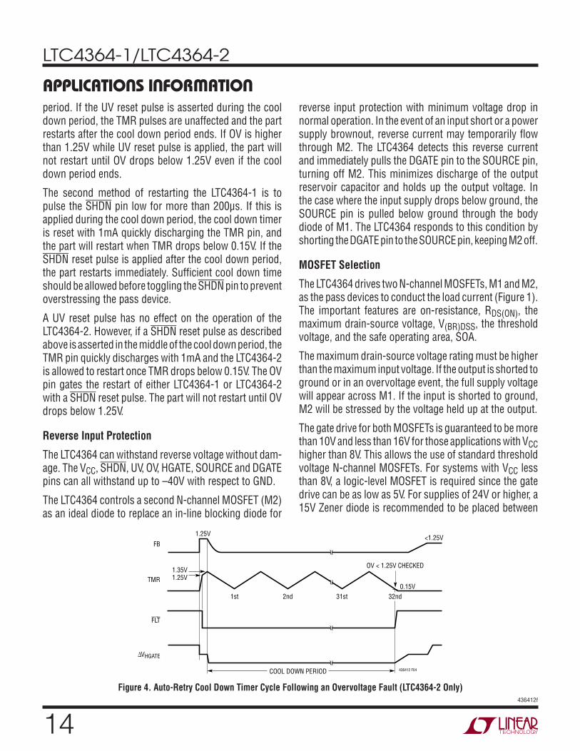
Cool Down Period and Restart
As soon as TMR reaches 1.35V and HGATE pulls low in a fault condition, the TMR pin starts discharging with a 2μA current. When the TMR pin voltage drops to 0.15V, TMR charges with 2μA. When TMR reaches 1.35V, it starts discharging again with 2μA. This pattern repeats 32 times to form a long cool down timer period before retry (Fig-ure 4). At the end of the cool down period (when the TMR pin voltage drops to 0.15V the 32nd time), the voltage at the OV pin is checked. If the OV voltage is above its 1.25V threshold, retry is inhibited and the HGATE pin remains low. If the OV pin voltage is below 1.25V minus the OV hysteresis, the LTC4364-2 retries, pulling the HGATE pin up and turning on the pass device M1. The FLT pin will then go to a high impedance state. The total cool down timer period is given by:
tCOOL =
63 •CTMR •1.2V2µA
The latch-off version, LTC4364-1, latches the HGATE and FLT pins low after a fault timeout. It also generates the cool down TMR pulses as shown in Figure 4, but does not retry after the cool down period. There are two ways to restart the part. The first method is to pull the UV pin below 0.6V momentarily (>10μs) after the cool down timer
APPLICATIONS INFORMATION
LTC4364-1/LTC4364-2
14436412f
period. If the UV reset pulse is asserted during the cool down period, the TMR pulses are unaffected and the part restarts after the cool down period ends. If OV is higher than 1.25V while UV reset pulse is applied, the part will not restart until OV drops below 1.25V even if the cool down period ends.
The second method of restarting the LTC4364-1 is to pulse the SHDN pin low for more than 200μs. If this is applied during the cool down period, the cool down timer is reset with 1mA quickly discharging the TMR pin, and the part will restart when TMR drops below 0.15V. If the SHDN reset pulse is applied after the cool down period, the part restarts immediately. Sufficient cool down time should be allowed before toggling the SHDN pin to prevent overstressing the pass device.
A UV reset pulse has no effect on the operation of the LTC4364-2. However, if a SHDN reset pulse as described above is asserted in the middle of the cool down period, the TMR pin quickly discharges with 1mA and the LTC4364-2 is allowed to restart once TMR drops below 0.15V. The OV pin gates the restart of either LTC4364-1 or LTC4364-2 with a SHDN reset pulse. The part will not restart until OV drops below 1.25V.
Reverse Input Protection
The LTC4364 can withstand reverse voltage without dam-age. The VCC, SHDN, UV, OV, HGATE, SOURCE and DGATE pins can all withstand up to –40V with respect to GND.
The LTC4364 controls a second N-channel MOSFET (M2) as an ideal diode to replace an in-line blocking diode for
reverse input protection with minimum voltage drop in normal operation. In the event of an input short or a power supply brownout, reverse current may temporarily flow through M2. The LTC4364 detects this reverse current and immediately pulls the DGATE pin to the SOURCE pin, turning off M2. This minimizes discharge of the output reservoir capacitor and holds up the output voltage. In the case where the input supply drops below ground, the SOURCE pin is pulled below ground through the body diode of M1. The LTC4364 responds to this condition by shorting the DGATE pin to the SOURCE pin, keeping M2 off.
MOSFET Selection
The LTC4364 drives two N-channel MOSFETs, M1 and M2, as the pass devices to conduct the load current (Figure 1). The important features are on-resistance, RDS(ON), the maximum drain-source voltage, V(BR)DSS, the threshold voltage, and the safe operating area, SOA.
The maximum drain-source voltage rating must be higher than the maximum input voltage. If the output is shorted to ground or in an overvoltage event, the full supply voltage will appear across M1. If the input is shorted to ground, M2 will be stressed by the voltage held up at the output.
The gate drive for both MOSFETs is guaranteed to be more than 10V and less than 16V for those applications with VCC higher than 8V. This allows the use of standard threshold voltage N-channel MOSFETs. For systems with VCC less than 8V, a logic-level MOSFET is required since the gate drive can be as low as 5V. For supplies of 24V or higher, a 15V Zener diode is recommended to be placed between
1.35V1.25V
FB
TMR
∆VHGATE
FLT
1.25V <1.25V
1st 2nd 31st0.15V
32nd
436412 F04
OV < 1.25V CHECKED
COOL DOWN PERIOD
Figure 4. Auto-Retry Cool Down Timer Cycle Following an Overvoltage Fault (LTC4364-2 Only)
APPLICATIONS INFORMATION
LTC4364-1/LTC4364-2
15436412f
gate and source of each MOSFET for extra protection (Figures 8 to 10).
Transient Stress in the MOSFET
The SOA of the MOSFET must encompass all fault condi-tions. In normal operation the pass devices are fully on, dissipating very little power. But during either overvoltage or overcurrent faults, the HGATE pin is controlled to regulate either the output voltage or the current through MOSFET M1. Large current and high voltage drop across M1 can coexist in these cases. The SOA curves of the MOSFET must be considered carefully along with the selection of the fault timer capacitor.
During an overvoltage event, the LTC4364 drives the pass MOSFET M1 to regulate the output voltage at an acceptable level. The load circuitry may continue operating throughout this interval, but only at the expense of dissipation in the MOSFET pass device. MOSFET dissipation or stress is a function of the input voltage waveform, regulation voltage and load current. The MOSFET must be sized to survive this stress.
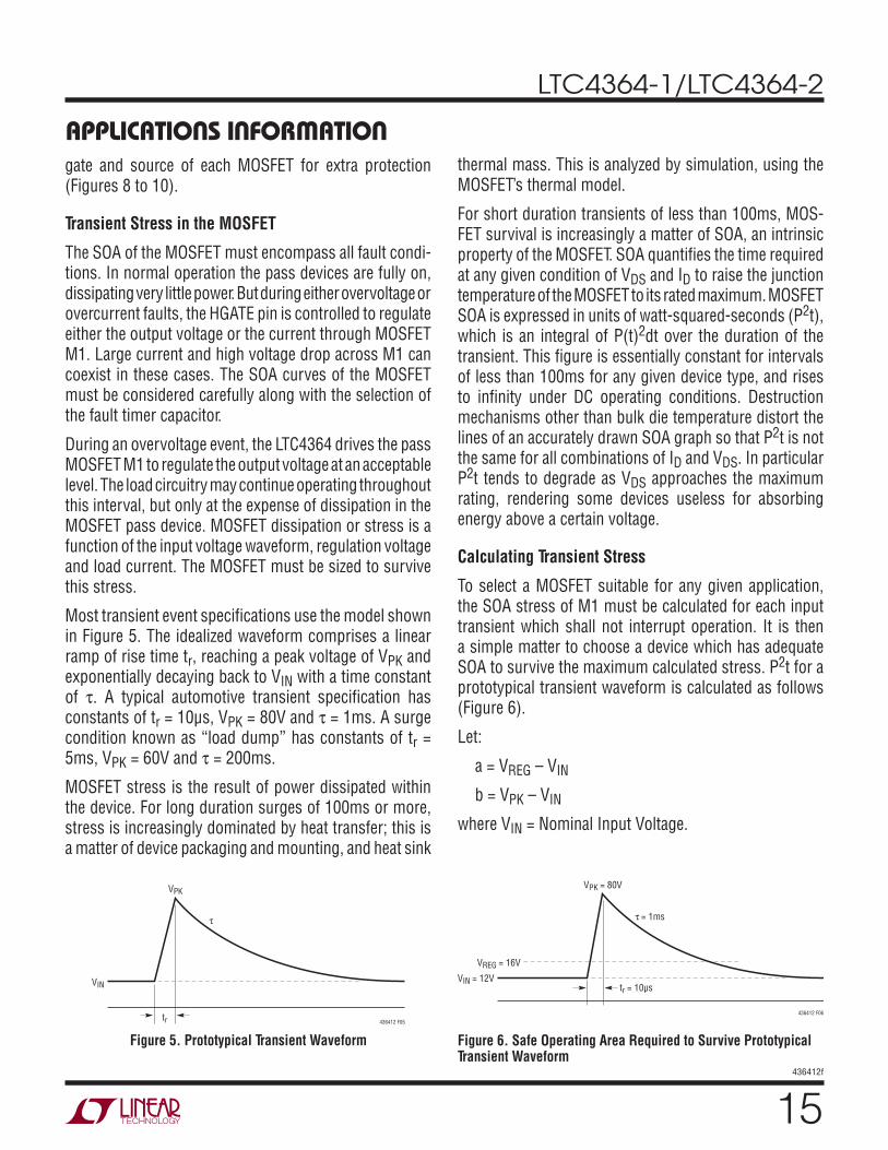
Most transient event specifications use the model shown in Figure 5. The idealized waveform comprises a linear ramp of rise time tr, reaching a peak voltage of VPK and exponentially decaying back to VIN with a time constant of τ. A typical automotive transient specification has constants of tr = 10μs, VPK = 80V and τ = 1ms. A surge condition known as “load dump” has constants of tr = 5ms, VPK = 60V and τ = 200ms.
MOSFET stress is the result of power dissipated within the device. For long duration surges of 100ms or more, stress is increasingly dominated by heat transfer; this is a matter of device packaging and mounting, and heat sink
thermal mass. This is analyzed by simulation, using the MOSFET’s thermal model.
For short duration transients of less than 100ms, MOS-FET survival is increasingly a matter of SOA, an intrinsic property of the MOSFET. SOA quantifies the time required at any given condition of VDS and ID to raise the junction temperature of the MOSFET to its rated maximum. MOSFET SOA is expressed in units of watt-squared-seconds (P2t), which is an integral of P(t)2dt over the duration of the transient. This figure is essentially constant for intervals of less than 100ms for any given device type, and rises to infinity under DC operating conditions. Destruction mechanisms other than bulk die temperature distort the lines of an accurately drawn SOA graph so that P2t is not the same for all combinations of ID and VDS. In particular P2t tends to degrade as VDS approaches the maximum rating, rendering some devices useless for absorbing energy above a certain voltage.
Calculating Transient Stress
To select a MOSFET suitable for any given application, the SOA stress of M1 must be calculated for each input transient which shall not interrupt operation. It is then a simple matter to choose a device which has adequate SOA to survive the maximum calculated stress. P2t for a prototypical transient waveform is calculated as follows (Figure 6).
Let:
a = VREG – VIN
b = VPK – VIN
where VIN = Nominal Input Voltage.
VPK
τ
VIN
436412 F05tr
Figure 5. Prototypical Transient Waveform Figure 6. Safe Operating Area Required to Survive Prototypical Transient Waveform
VPK = 80V
τ = 1ms
VIN = 12V
436412 F06
VREG = 16V
tr = 10µs
APPLICATIONS INFORMATION

LTC4364-1/LTC4364-2
16436412f
Then:
P2t = ILOAD2 1
3tr
b − a( )3
b+ 1
2τ 2a2In
ba
+ 3a2 + b2 – 4ab
Typically VREG ≈ VIN and τ >> tr simplifying the above to:
P2t = 1
2ILOAD
2 VPK − VREG( )2 τ
For the transient conditions of VPK = 80V, VIN = 12V, VREG = 16V, tr = 10μs and τ = 1ms, and a load current of 3A, P2t is 18.4W2s—easily handled by a MOSFET in a D-pak package. The P2t of other transient waveshapes is evalu-ated by integrating the square of MOSFET power versus time. LTSpice™ can be used to simulate timer behavior for more complex transients and cases where overvoltage and overcurrent faults coexist.
Short-Circuit Stress
SOA stress of M1 must also be calculated for output short-circuit conditions. Short-circuit P2t is given by:
P2t = VIN •
∆VSNSRSNS
2
• tOC
where ∆VSNS is the overcurrent fault threshold and tOC is the overcurrent timer interval.
For VIN = 15V, OUT = 0V, ∆VSNS = 25mV, RSNS = 12mΩ and CTMR = 100nF, P2t is 2.2W2s—less than the transient SOA calculated in the previous example. Nevertheless, to account for circuit tolerances this figure should be doubled to 4.4W2s.
Limiting Inrush Current and HGATE Pin Compensation
The LTC4364 limits the inrush current to any load capaci-tance by controlling the HGATE pin voltage slew rate. An external capacitor, CHG, can be connected from HGATE to ground to slow down the inrush current further at the expense of slower turn-off time. The gate capacitor is set at:
CHG =
IHGATE(UP)
IINRUSH•CL
where IHGATE(UP) is the HGATE pin pull-up current, IINRUSH is the desired inrush current, CL is total load capacitance at the output. In typical applications, a CHG of 6.8nF is recommended for loop compensation during overvoltage and overcurrent events. With input voltage steps faster than 5V/μs, a larger gate capacitor helps prevent self enhancement of the N-channel MOSFET.
The added gate capacitor slows down the turn-off time during fault conditions and allows higher peak currents to build up during an output short event. If this is a concern, an extra resistor, R6, in series with CHG can restore the turn-off time. A diode, D5, should be placed across R6 with the cathode connected to CHG as shown in Figure 1. In a fast transient input step, D5 provides a bypass path to CHG for the benefit of holding HGATE low and preventing self enhancement.
Shutdown
The LTC4364 can be shut down to a low current mode by pulling SHDN below 0.5V. The quiescent VCC current drops to 10μA for both the LTC4364-1 and the LTC4364-2.
The SHDN pin can be pulled up to 100V or below GND by up to 40V without damage. Leaving the pin open allows an internal current source to pull it up to about 4V and turn the part on. The leakage current at the pin should be limited to no more than 1μA if no pull-up device is used to help turn it on.
Supply Transient Protection
The LTC4364 is tested to operate to 80V and guaranteed to be safe from damage between 100V and −40V. Voltage transients above 100V or below −40V may cause permanent damage. During a short-circuit condition, the large change in current flowing through power supply traces coupled with parasitic inductances from associated wiring can cause destructive voltage transients in both positive and negative directions at the VCC, SOURCE, and OUT pins. To reduce the voltage transients, minimize the power trace parasitic inductance by using short, wide traces. A small RC filter (R4 and C1 in Figure 1) at the VCC pin filters high voltage spikes of short pulse width.
APPLICATIONS INFORMATION

LTC4364-1/LTC4364-2
17436412f
Another way to limit supply transients above 100V at the VCC pin is to use a Zener diode and a resistor, D1 and R4, as shown in Figure 1. D1 clamps voltage spikes at the VCC pin while R4 limits the current through D1 to a safe level during the surge. In the negative direction, D1 along with R4 clamps the VCC pin near GND. The inclusion of R4 in series with the VCC pin increases the minimum required supply voltage due to the extra voltage drop across the resistor, which is determined by the supply current of the LTC4364 and the leakage current of D1. 2.2k adds about 1V to the minimum operating voltage.
For sustained, elevated suppy voltages, the power dissipa-tion of R4 becomes unacceptable. This can be resolved by using an external NPN transistor (Q1 in Figure 7) as a buffer. To protect Q1 against supply reversal, block the collector of Q1 with a series diode or tie it to the cathode of D3 and D4 in Figure 1.
Transient suppressor D3 in Figure 1 clamps the input voltage to 200V for voltage transients higher than 200V, to prevent breakdown of M1. It also blocks forward con-duction in D4. D4 limits the SOURCE pin voltage to 24V below GND when the input goes negative. COUT helps absorb the inductive energy at the output upon a sudden input short, protecting the OUT and SENSE pins.
Output Port Protection
In applications where the output is on a connector, as shown in Figure 14, if the output is plugged into a supply that is higher than the input, the ideal diode MOSFET, M2, turns off to open the backfeeding path. In the case where the output port is plugged into a supply that is below GND, the SOURCE pin is pulled below GND through the body diode of M2. The LTC4364 responds to this condition by shorting the HGATE pin to the SOURCE pin, turning M1 off and shutting down the current path from VIN to VOUT.
Design Example
As a design example, consider an application with the following specifications: VIN = 8V to 14V DC with a peak transient of 200V and decay time constant τ of 1ms, VOUT ≤ 27V, minimum current limit ILIM(MIN) at 4A, low-battery detection at 6V, input overvoltage level at 60V, and 1ms of overvoltage early warning (Figure 1).
Selection of CMZ5945B for D1 will limit the voltage at the VCC pin to less than 71V during the 200V surge. The minimum required voltage at the VCC pin is 4V when VIN is at 6V; the maximum supply current for LTC4364 is 750μA. The maximum value for R4 to ensure proper operation is:
R4 = 6V – 4V
0.75mA= 2.7k
Select 2.2k for R4 to accommodate all conditions.
With the minimum Zener voltage at 64V, the peak current through R4 into D1 is then calculated as:
ID1(PK) = 200V – 64V
2.2k= 62mA
which can be handled by the CMZ5945B with a peak power rating of 200W at 10/1000μs.
With a bypass capacitance of 0.1μF (C1), along with R4 of 2.2k, high voltage transients up to 250V with a pulse width less than 20μs are filtered out at the VCC pin.
Next, calculate the resistive divider value to limit VOUT to 27V during an overvoltage event:
VREG =
1.25V • R7 + R8( )R8
= 27V
APPLICATIONS INFORMATION
VCC
LTC4364
GND
436412 F07
C1100nF
Q1PZTA42
VIN200V
D1CMZ5945B68V
R422k1/4W
Figure 7. Buffering VCC to Extend Input Supply Range
Output Bypassing
The OUT and SENSE pins can withstand up to 100V above and 20V below GND. In all applications the output must be bypassed with at least 22μF low ESR electrolytic (COUT in Figure 1) to stabilize the voltage and current limiting loops, and to minimize capacitive feedthrough of input transients. Total ceramic bypassing of up to one-tenth the total electrolytic capacitance is permissible without compromising performance.
LTC4364-1/LTC4364-2
18436412f
Choosing 250μA for the resistive divider:
R8 = 1.25V
250µA= 5k
Select 4.99k for R8.
R7 =
27V –1.25V( ) •R81.25V
= 102.8k
The closest standard value for R7 is 102k.
Now, calculate the sense resistor, RSNS, value:
RSNS =
∆VSNS(MIN)
ILIM= 45mV
4A= 11mΩ
Choose 10mΩ for RSNS.
CTMR is then chosen for 1ms of early warning time:
CTMR = 1ms•5µA
100mV= 50nF
The closest standard value for CTMR is 47nF.
Finally, calculate R1, R2 and R3 for 6V low battery detec-tion and 60V input overvoltage level:
6VR1+ R2 + R3
= 1.25VR2 + R3
60VR1+ R2 + R3
= 1.25VR3
Simplify the equations and choose 10k for R3 to get:
R2 = 60V6V
–1
•R3 = 9 •R3 = 90k
R1= 6V1.25V
–1
• R2+R3( ) = 3.8 • R1+R2( ) = 380k
Select 90.9kΩ for R2 and 383kΩ for R1.
The pass device, M1, should be chosen to withstand an output short condition with VCC = 14V. In the case of a severe output short where VOUT = 0V, ITMR(UP) = 55μA and the total overcurrent fault time is:
tOC =
CTMR • VTMR(G)
ITRM(UP)= 47nF •1.35V
55µA= 1.15ms
The maximum power dissipation in M1 is:
P =
∆VDS(M1) • ∆VSNS(MAX)
RSNS= 14V •32mV
10mΩ= 45W
The corresponding P2t is 2.3W2s.
During an output overload or soft short, the voltage at the OUT pin could stay at 2V or higher. The total overcurrent fault time when VOUT = 2V is:
tOC = 47nF •1.35V
49µA= 1.3ms
The maximum power dissipation in M1 is:
P =
14V – 2V( ) •55mV10mΩ
= 66W
The corresponding P2t is 5.7W2s. Both of the above condi-tions are well within the safe operating area of FDB33N25.
To select the pass device, M2, first calculate RDS(ON) to achieve the desired forward drop VFW at maximum load current (5.5A). If VFW = 0.25V:
RDS(ON) ≤
VFWILOAD(MAX)
= 0.25V5.5A
= 45.5mΩ
The FDB3682 offers a maximum RDS(ON) of 36mΩ at VGS = 10V so is a good fit. Its minimum BVDSS of 100V is also sufficient to handle VOUT transients up to 100V during an input short-circuit event.
Layout Considerations
To achieve accurate current sensing, use Kelvin connections to the current sense resistor, RSNS. Limit the resistance from the SOURCE pin to the sources of the MOSFETs to below 10Ω. The minimum trace width for 1oz copper foil is 0.02" per amp to ensure the trace stays at a reason-able temperature. Note that 1oz copper exhibits a sheet resistance of about 530μΩ/square. Small resistances can cause large errors in high current applications. Noise im-munity will be improved significantly by locating resistive dividers close to the pins with short VCC and GND traces.
APPLICATIONS INFORMATION

LTC4364-1/LTC4364-2
19436412f
TYPICAL APPLICATIONS
Figure 8. 2A Wide Range Hot Swap Controller with Circuit Breaker
Figure 9. 28V Hot Swap with Overvoltage Output Regulation at 27V, Circuit Breaker, and Reverse Current Protection
Figure 10. 48V Hot Swap with Overvoltage Output Regulation at 72V, Circuit Breaker, and Reverse Current Protection
+
OUTSENSEDGATESOURCEHGATE
TMRGND
CTMR0.22µF
UV
OV ENOUT
436412 F08
FLT
SHDN FB
R510Ω
VIN5V TO 28V
R244.2k
R1118k
UV4.2V
OV36V
D1SMAT70A
R35.9k
CLOAD100µF
VOUT2A
M1SUD50N03-9
RSNS20mΩ
CHG47nF
D6DDZ9702T
VCC
LTC4364
+
OUTSENSEDGATESOURCEHGATE
TMRGND
CTMR0.1µF
UV
OV ENOUT
436412 F09
FLT
SHDN FB
R510Ω
R84.02k
VIN18V TO 33V
R26.04k
OV45V
UV15V
R1100k
R33.01k
CLOAD100µF
VOUT2.5ACLAMPEDAT 36V
M1FDB3632
D6DDZ9702T
M2FDMS86101
RSNS15mΩ
CHG47nF
VCC
LTC4364
R7110k
D7DDZ9702T
+
OUTSENSEDGATESOURCEHGATE
TMRGND
CTMR0.1µF
UV
OV ENOUT
436412 F10
FLT
SHDN FB
R510ΩR4
2.2k
VIN36V TO 72V
R1205k
UV36V
OV76V
R23.92k
R33.48k
R7226k
R84.02k
CLOAD330µF
VOUT4ACLAMPEDAT 72V
D1CMZ5945B
68V
M1FDB33N25
M2FDB3632
RSNS10mΩ
CHG47nF
VCC
LTC4364
D6DDZ9702T
D7DDZ9702T

LTC4364-1/LTC4364-2
20436412f
TYPICAL APPLICATIONS
Figure 11. Redundant Supply Diode-OR with Overvoltage Surge Protection
Figure 12. High Side Switch with Ideal Diode for Load Protection
+
OUTSENSEDGATESOURCEHGATE
TMRCTMRA0.22µF
UV
OVENOUT
FLT
SHDN FB
R5A10Ω
VINA12V
R7A59k
R8A4.99k
COUTA22µF
VOUTCLAMPEDAT 16V
M1AFDD16AN08A0
M2AFDD16AN08A0
RSNSA10mΩ
CHGA6.8nF
VCC
LTC4364
+
OUTSENSEDGATESOURCEHGATE
TMRCTMRB0.22µF
UV
OVENOUT
FLT
SHDN FB
R5B10Ω
VINB12V
R7B59k
R8B4.99k
436412 F11
COUTB22µF
M1BFDD16AN08A0
M2BFDD16AN08A0
RSNSB10mΩ
CHGB6.8nF
VCC
LTC4364
GND
GND
OUTSENSEDGATESOURCEHGATE
TMR GND
UVSHDN M3VN2222
100k
OV ENOUT
436412 F12
FLT
SHDN FB
VIN12V
CLOAD
VOUT
M1FDB3632
M2FDMS86101
VCC
LTC4364
LTC4364-1/LTC4364-2
21436412f
TYPICAL APPLICATIONS
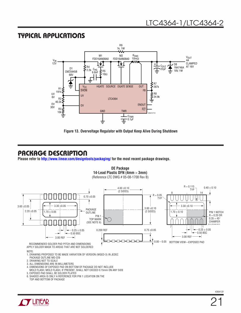
Figure 13. Overvoltage Regulator with Output Keep Alive During Shutdown
PACKAGE DESCRIPTION
DE Package14-Lead Plastic DFN (4mm × 3mm)
(Reference LTC DWG # 05-08-1708 Rev B)
Please refer to http://www.linear.com/designtools/packaging/ for the most recent package drawings.
3.00 ±0.10(2 SIDES)
4.00 ±0.10(2 SIDES)
NOTE:1. DRAWING PROPOSED TO BE MADE VARIATION OF VERSION (WGED-3) IN JEDEC PACKAGE OUTLINE MO-2292. DRAWING NOT TO SCALE 3. ALL DIMENSIONS ARE IN MILLIMETERS4. DIMENSIONS OF EXPOSED PAD ON BOTTOM OF PACKAGE DO NOT INCLUDE MOLD FLASH. MOLD FLASH, IF PRESENT, SHALL NOT EXCEED 0.15mm ON ANY SIDE5. EXPOSED PAD SHALL BE SOLDER PLATED6. SHADED AREA IS ONLY A REFERENCE FOR PIN 1 LOCATION ON THE TOP AND BOTTOM OF PACKAGE
0.40 ± 0.10
BOTTOM VIEW—EXPOSED PAD
1.70 ± 0.10
0.75 ±0.05
R = 0.115TYP
R = 0.05TYP
3.00 REF
17
148
PIN 1TOP MARK
(SEE NOTE 6)
0.200 REF
0.00 – 0.05
(DE14) DFN 0806 REV B
PIN 1 NOTCHR = 0.20 OR0.35 × 45°CHAMFER
0.25 ± 0.050.50 BSC
3.30 ±0.10
1.70 ± 0.05
3.00 REF
RECOMMENDED SOLDER PAD PITCH AND DIMENSIONSAPPLY SOLDER MASK TO AREAS THAT ARE NOT SOLDERED
2.20 ±0.05
0.70 ±0.05
3.60 ±0.05PACKAGEOUTLINE
0.25 ± 0.05
3.30 ±0.05
0.50 BSC
+
OUTSENSEDGATESOURCEHGATE
TMRGND
CTMR0.1µF
UV
OV ENOUT
436412 F13
FLT
SHDN FB
R42.2k R5
10Ω
VIN12V
R1191k
UV6V
OV30V
R240.2k
R310k
R7287k
R824.9k
COUT22µF
D81N4746A18V, 1W
VOUT4ACLAMPEDAT 16V
D1CMZ5945B
68V
M1FDD16AN08A0
M2FDD16AN08A0
RSNS10mΩ
R91k, 1W
CHG6.8nF
VCC
LTC4364

LTC4364-1/LTC4364-2
22436412f
MS Package16-Lead Plastic MSOP
(Reference LTC DWG # 05-08-1669 Rev Ø)
MSOP (MS16) 1107 REV Ø
0.53 ± 0.152(.021 ± .006)
SEATINGPLANE
0.18(.007)
1.10(.043)MAX
0.17 – 0.27(.007 – .011)
TYP
0.86(.034)REF
0.50(.0197)
BSC
16151413121110
1 2 3 4 5 6 7 8
9
NOTE:1. DIMENSIONS IN MILLIMETER/(INCH)2. DRAWING NOT TO SCALE3. DIMENSION DOES NOT INCLUDE MOLD FLASH, PROTRUSIONS OR GATE BURRS. MOLD FLASH, PROTRUSIONS OR GATE BURRS SHALL NOT EXCEED 0.152mm (.006") PER SIDE4. DIMENSION DOES NOT INCLUDE INTERLEAD FLASH OR PROTRUSIONS. INTERLEAD FLASH OR PROTRUSIONS SHALL NOT EXCEED 0.152mm (.006") PER SIDE5. LEAD COPLANARITY (BOTTOM OF LEADS AFTER FORMING) SHALL BE 0.102mm (.004") MAX
0.254(.010) 0° – 6° TYP
DETAIL “A”
DETAIL “A”
GAUGE PLANE
5.23(.206)MIN
3.20 – 3.45(.126 – .136)
0.889 ± 0.127(.035 ± .005)
RECOMMENDED SOLDER PAD LAYOUT
0.305 ± 0.038(.0120 ± .0015)
TYP
0.50(.0197)
BSC
4.039 ± 0.102(.159 ± .004)
(NOTE 3)
0.1016 ± 0.0508(.004 ± .002)
3.00 ± 0.102(.118 ± .004)
(NOTE 4)
0.280 ± 0.076(.011 ± .003)
REF
4.90 ± 0.152(.193 ± .006)
PACKAGE DESCRIPTIONPlease refer to http://www.linear.com/designtools/packaging/ for the most recent package drawings.

LTC4364-1/LTC4364-2
23436412f
Information furnished by Linear Technology Corporation is believed to be accurate and reliable. However, no responsibility is assumed for its use. Linear Technology Corporation makes no representa-tion that the interconnection of its circuits as described herein will not infringe on existing patent rights.
PACKAGE DESCRIPTIONPlease refer to http://www.linear.com/designtools/packaging/ for the most recent package drawings.
.016 – .050(0.406 – 1.270)
.010 – .020(0.254 – 0.508)
× 45°
0° – 8° TYP.008 – .010
(0.203 – 0.254)
1
N
2 3 4 5 6 7 8
N/2
.150 – .157(3.810 – 3.988)
NOTE 3
16 15 14 13
.386 – .394(9.804 – 10.008)
NOTE 3
.228 – .244(5.791 – 6.197)
12 11 10 9
S16 REV G 0212
.053 – .069(1.346 – 1.752)
.014 – .019(0.355 – 0.483)
TYP
.004 – .010(0.101 – 0.254)
.050(1.270)
BSC
.245MIN
N
1 2 3 N/2
.160 ±.005
RECOMMENDED SOLDER PAD LAYOUT
.045 ±.005 .050 BSC
.030 ±.005 TYP
INCHES(MILLIMETERS)
NOTE:1. DIMENSIONS IN
2. DRAWING NOT TO SCALE3. THESE DIMENSIONS DO NOT INCLUDE MOLD FLASH OR PROTRUSIONS. MOLD FLASH OR PROTRUSIONS SHALL NOT EXCEED .006" (0.15mm)4. PIN 1 CAN BE BEVEL EDGE OR A DIMPLE
S Package16-Lead Plastic Small Outline (Narrow .150 Inch)
(Reference LTC DWG # 05-08-1610 Rev G)

LTC4364-1/LTC4364-2
24436412f
Linear Technology Corporation1630 McCarthy Blvd., Milpitas, CA 95035-7417 (408) 432-1900 FAX: (408) 434-0507 www.linear.com LINEAR TECHNOLOGY CORPORATION 2012
LT 0712 • PRINTED IN USA
RELATED PARTS
TYPICAL APPLICATION
PART NUMBER DESCRIPTION COMMENTS
LT®4356-1/LT4356-2 LT4356-3
Surge Stopper LT4356-1: 7A Shutdown Mode LT4356-2: Auxiliary Amplifier Alive in Shutdown Mode LT4356-3: Fault Latchoff
LTC4363 High Voltage Surge Stopper 4V to 80V, VCC Clamp, Adjustable Output Voltage Clamp, 60V Reverse Input Protection, Overcurrent Protection
LTC4366 Floating Surge Stopper 9V to >500V Operation, Adjustable Output Voltage Clamp
LTC4357 Positive High Voltage Ideal Diode Controller 0.5µs Turn-Off Time, 9V to 80V
LTC4359 Ideal Diode Controller with Reverse Input Protection 4V to 80V Operation, –40V Reverse-Input Protection, Low 13µA Shutdown Current
LTC4352 Ideal MOSFET ORing Diode External N-Channel MOSFETs Replace ORing Diodes, 0V to 18V
LTC4354 Negative Voltage Diode-OR Controller Controls Two N-Channel MOSFETs, 1µs Turn-Off, 80V Operation
LTC4355 Positive Voltage Diode-OR Controller Controls Two N-Channel MOSFETs, 0.5µs Turn-Off, 80V Operation
LTC4365 Window Passer - OV, UV and Reverse Supply Protection Controller
2.5V to 34V Operation, Protects 60V to –40V
Figure 14. 0.25A, 12V Surge Stopper with Output Port Protection
OUTSENSEDGATESOURCEHGATE
UV
OV
0.1µF
ENOUT
436412 F14
FLT
SHDN FB
R510Ω
VIN12V
R290.9k1%
R1383k1%UV
6V
OV60V R3
10k1%
*PROTECTED AGAINST BACKFEEDING OR FORWARD CONDUCTING FROM –20V TO 50V
VOUT*CLAMPEDAT 18V
M1FDB3632
M2FDMS86101
RSNS0.2Ω
CHG6.8nF
CIN10µF
10µF50VCER
10µF50VCER
VCC
LTC4364
GND TMR
R84.99k1%
R916.9k1%
RESR100mΩ
D2DDZ9702T15V
R749.9k1%