LT4363 - High Voltage Surge Stopper with Current...
24
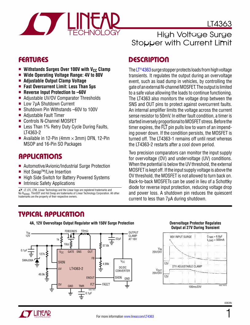
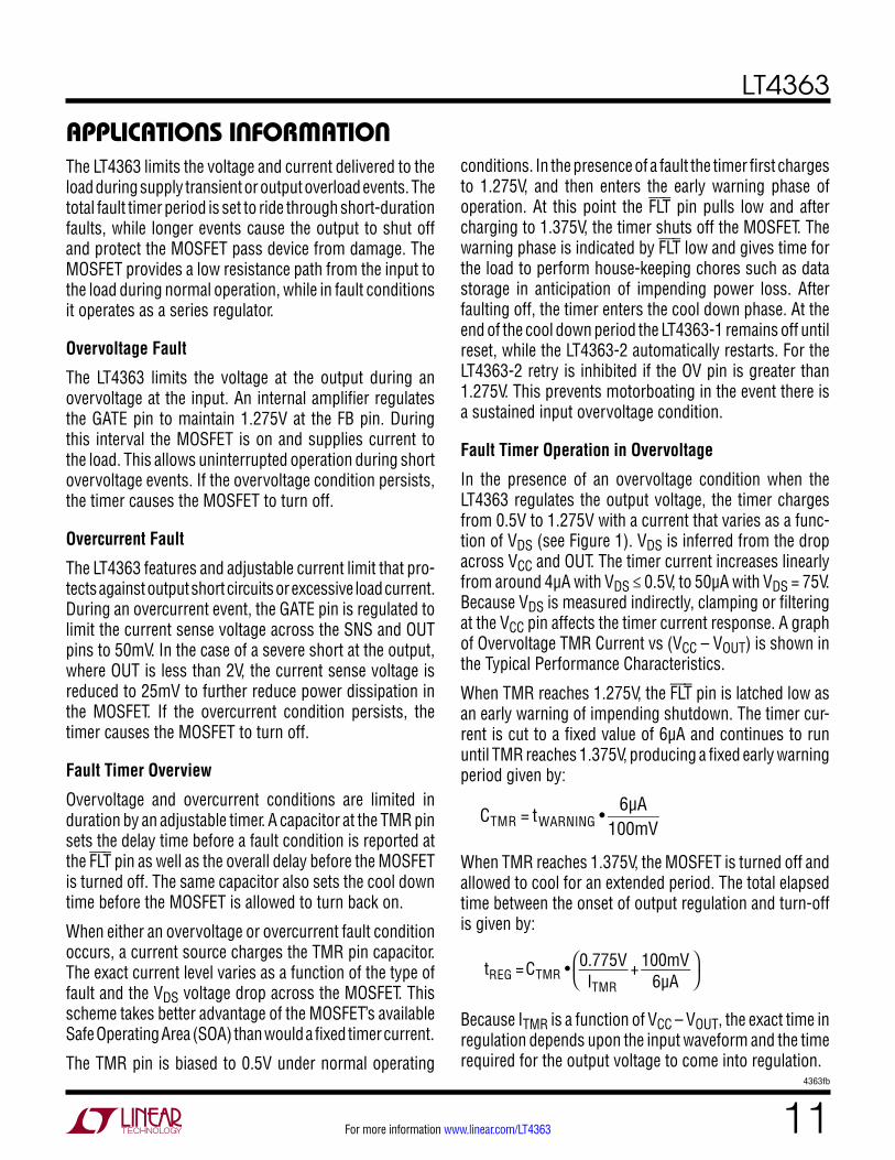
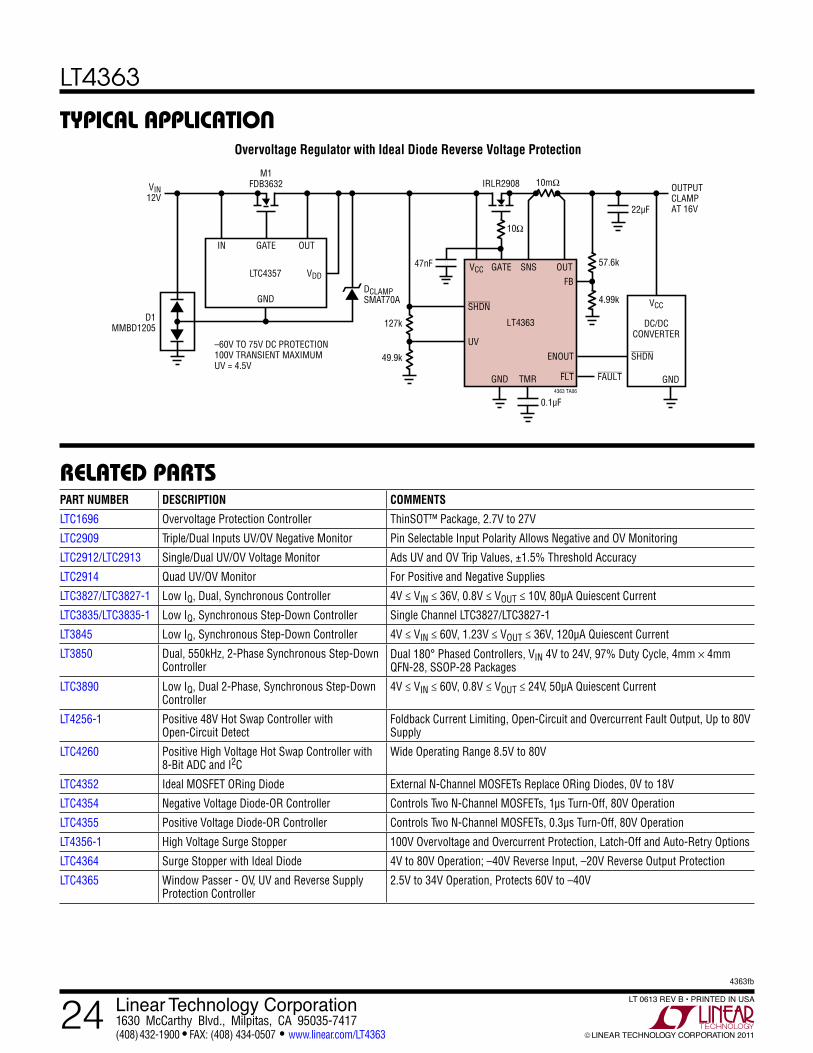
LT4363 1 4363fb For more information www.linear.com/LT4363 100ms/DIV 4363 TA01b V IN 20V/DIV V OUT 20V/DIV 80V INPUT SURGE C TMR = 6.8μF I LOAD = 500mA 27V ADJUSTABLE CLAMP 12V 12V The LT ® 4363 surge stopper protects loads from high voltage transients. It regulates the output during an overvoltage event, such as load dump in vehicles, by controlling the gate of an external N-channel MOSFET. The output is limited to a safe value allowing the loads to continue functioning. The LT4363 also monitors the voltage drop between the SNS and OUT pins to protect against overcurrent faults. An internal amplifier limits the voltage across the current sense resistor to 50mV. In either fault condition, a timer is started inversely proportional to MOSFET stress. Before the timer expires, the FLT pin pulls low to warn of an impend- ing power down. If the condition persists, the MOSFET is turned off. The LT4363-1 remains off until reset whereas the LT4363-2 restarts after a cool down period. Two precision comparators can monitor the input supply for overvoltage (OV) and undervoltage (UV) conditions. When the potential is below the UV threshold, the external MOSFET is kept off. If the input supply voltage is above the OV threshold, the MOSFET is not allowed to turn back on. Back-to-back MOSFETs can be used in lieu of a Schottky diode for reverse input protection, reducing voltage drop and power loss. A shutdown pin reduces the quiescent current to less than 7µA during shutdown. TYPICAL APPLICATION FEATURES DESCRIPTION High Voltage Surge Stopper with Current Limit 4A, 12V Overvoltage Output Regulator with 150V Surge Protection Overvoltage Protector Regulates Output at 27V During Transient APPLICATIONS n Withstands Surges Over 100V with V CC Clamp n Wide Operating Voltage Range: 4V to 80V n Adjustable Output Clamp Voltage n Fast Overcurrent Limit: Less Than 5µs n Reverse Input Protection to –60V n Adjustable UV/OV Comparator Thresholds n Low 7µA Shutdown Current n Shutdown Pin Withstands –60V to 100V n Adjustable Fault Timer n Controls N-Channel MOSFET n Less Than 1% Retry Duty Cycle During Faults, LT4363-2 n Available in 12-Pin (4mm × 3mm) DFN, 12-Pin MSOP and 16-Pin SO Packages n Automotive/Avionic/Industrial Surge Protection n Hot Swap™/Live Insertion n High Side Switch for Battery Powered Systems n Intrinsic Safety Applications L, LT, LTC, LTM, Linear Technology and the Linear logo are registered trademarks and No R SENSE , ThinSOT and Hot Swap are trademarks of Linear Technology Corporation. All other trademarks are the property of their respective owners. 0.1μF 10Ω 10mΩ FDB33N25 V IN 12V 4363 TA01 LT4363-2 GND TMR OUT GATE SNS UV SHDN OV FAULT OUTPUT CLAMP AT 16V ENOUT FLT FB 1k SMAJ58A 22μF 0.1μF V CC DC/DC CONVERTER GND SHDN V CC 4.99k 127k 49.9k 57.6k
Transcript of LT4363 - High Voltage Surge Stopper with Current...
LT4363
14363fb
For more information www.linear.com/LT4363
100ms/DIV4363 TA01b
VIN20V/DIV
VOUT20V/DIV
80V INPUT SURGE CTMR = 6.8µFILOAD = 500mA
27V ADJUSTABLE CLAMP12V
12V
The LT®4363 surge stopper protects loads from high voltage transients. It regulates the output during an overvoltage event, such as load dump in vehicles, by controlling the gate of an external N-channel MOSFET. The output is limited to a safe value allowing the loads to continue functioning. The LT4363 also monitors the voltage drop between the SNS and OUT pins to protect against overcurrent faults. An internal amplifier limits the voltage across the current sense resistor to 50mV. In either fault condition, a timer is started inversely proportional to MOSFET stress. Before the timer expires, the FLT pin pulls low to warn of an impend-ing power down. If the condition persists, the MOSFET is turned off. The LT4363-1 remains off until reset whereas the LT4363-2 restarts after a cool down period.
Two precision comparators can monitor the input supply for overvoltage (OV) and undervoltage (UV) conditions. When the potential is below the UV threshold, the external MOSFET is kept off. If the input supply voltage is above the OV threshold, the MOSFET is not allowed to turn back on. Back-to-back MOSFETs can be used in lieu of a Schottky diode for reverse input protection, reducing voltage drop and power loss. A shutdown pin reduces the quiescent current to less than 7µA during shutdown.
Typical applicaTion
FeaTures DescripTion
High Voltage Surge Stopper with Current Limit
4A, 12V Overvoltage Output Regulator with 150V Surge Protection Overvoltage Protector Regulates Output at 27V During Transient
applicaTions
n Withstands Surges Over 100V with VCC Clampn Wide Operating Voltage Range: 4V to 80Vn Adjustable Output Clamp Voltagen Fast Overcurrent Limit: Less Than 5µsn Reverse Input Protection to –60Vn Adjustable UV/OV Comparator Thresholdsn Low 7µA Shutdown Currentn Shutdown Pin Withstands –60V to 100Vn Adjustable Fault Timern Controls N-Channel MOSFETn Less Than 1% Retry Duty Cycle During Faults,
LT4363-2n Available in 12-Pin (4mm × 3mm) DFN, 12-Pin
MSOP and 16-Pin SO Packages
n Automotive/Avionic/Industrial Surge Protectionn Hot Swap™/Live Insertionn High Side Switch for Battery Powered Systemsn Intrinsic Safety ApplicationsL, LT, LTC, LTM, Linear Technology and the Linear logo are registered trademarks and No RSENSE, ThinSOT and Hot Swap are trademarks of Linear Technology Corporation. All other trademarks are the property of their respective owners.
0.1µF
10Ω
10mΩFDB33N25VIN12V
4363 TA01
LT4363-2
GND TMR
OUTGATE SNS
UV
SHDN
OV FAULT
OUTPUT CLAMP AT 16V
ENOUT
FLT
FB
1k
SMAJ58A
22µF
0.1µF VCC
DC/DCCONVERTER
GNDSHDN
VCC4.99k
127k
49.9k
57.6k
LT4363
24363fb
For more information www.linear.com/LT4363
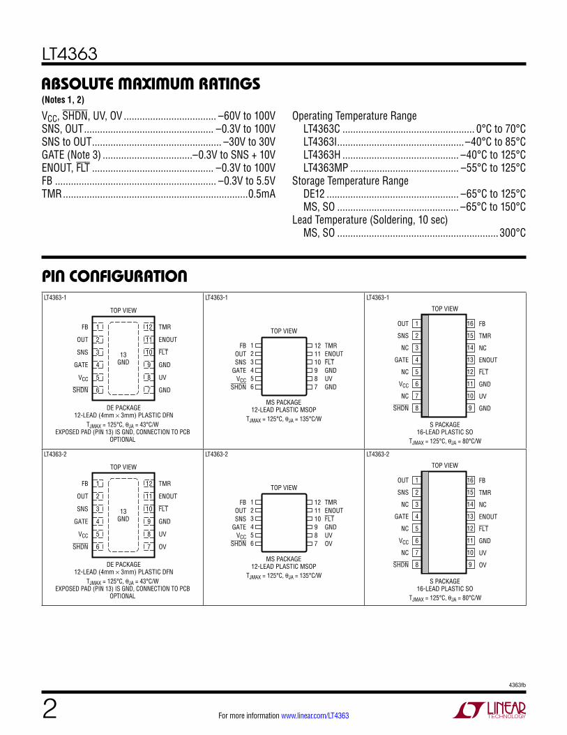
absoluTe MaxiMuM raTings
VCC, SHDN, UV, OV ................................... –60V to 100VSNS, OUT ................................................. –0.3V to 100VSNS to OUT ................................................. –30V to 30VGATE (Note 3) ..................................–0.3V to SNS + 10VENOUT, FLT .............................................. –0.3V to 100VFB ............................................................. –0.3V to 5.5VTMR ......................................................................0.5mA
(Notes 1, 2)
LT4363-1 LT4363-1 LT4363-1
12
11
10
9
8
7
13GND
1
2
3
4
5
6
TMR
ENOUT
FLT
GND
UV
GND
FB
OUT
SNS
GATE
VCC
SHDN
TOP VIEW
DE PACKAGE12-LEAD (4mm × 3mm) PLASTIC DFN
TJMAX = 125°C, θJA = 43°C/W EXPOSED PAD (PIN 13) IS GND, CONNECTION TO PCB
OPTIONAL
123456
FBOUTSNS
GATEVCC
SHDN
121110987
TMRENOUTFLTGNDUVGND
TOP VIEW
MS PACKAGE12-LEAD PLASTIC MSOP
TJMAX = 125°C, θJA = 135°C/W
TOP VIEW
S PACKAGE16-LEAD PLASTIC SO
1
2
3
4
5
6
7
8
16
15
14
13
12
11
10
9
OUT
SNS
NC
GATE
NC
VCC
NC
SHDN
FB
TMR
NC
ENOUT
FLT
GND
UV
GND
TJMAX = 125°C, θJA = 80°C/W
LT4363-2 LT4363-2 LT4363-2
12
11
10
9
8
7
13GND
1
2
3
4
5
6
TMR
ENOUT
FLT
GND
UV
OV
FB
OUT
SNS
GATE
VCC
SHDN
TOP VIEW
DE PACKAGE12-LEAD (4mm × 3mm) PLASTIC DFN
TJMAX = 125°C, θJA = 43°C/W EXPOSED PAD (PIN 13) IS GND, CONNECTION TO PCB
OPTIONAL
123456
FBOUTSNS
GATEVCC
SHDN
121110987
TMRENOUTFLTGNDUVOV
TOP VIEW
MS PACKAGE12-LEAD PLASTIC MSOP
TJMAX = 125°C, θJA = 135°C/W
TOP VIEW
S PACKAGE16-LEAD PLASTIC SO
1
2
3
4
5
6
7
8
16
15
14
13
12
11
10
9
OUT
SNS
NC
GATE
NC
VCC
NC
SHDN
FB
TMR
NC
ENOUT
FLT
GND
UV
OV
TJMAX = 125°C, θJA = 80°C/W
pin conFiguraTion
Operating Temperature Range LT4363C .................................................. 0°C to 70°C LT4363I ................................................–40°C to 85°C
LT4363H ............................................ –40°C to 125°C LT4363MP ......................................... –55°C to 125°CStorage Temperature Range
DE12 .................................................. –65°C to 125°C MS, SO .............................................. –65°C to 150°C
Lead Temperature (Soldering, 10 sec) MS, SO ............................................................. 300°C
LT4363
34363fb
For more information www.linear.com/LT4363
orDer inForMaTionLEAD FREE FINISH TAPE AND REEL PART MARKING* PACKAGE DESCRIPTION TEMPERATURE RANGE
LT4363CDE-1#PBF LT4363CDE-1#TRPBF 43631 12-Lead (4mm × 3mm) Plastic DFN 0°C to 70°C
LT4363IDE-1#PBF LT4363IDE-1#TRPBF 43631 12-Lead (4mm × 3mm) Plastic DFN –40°C to 85°C
LT4363HDE-1#PBF LT4363HDE-1#TRPBF 43631 12-Lead (4mm × 3mm) Plastic DFN –40°C to 125°C
LT4363CDE-2#PBF LT4363CDE-2#TRPBF 43632 12-Lead (4mm × 3mm) Plastic DFN 0°C to 70°C
LT4363IDE-2#PBF LT4363IDE-2#TRPBF 43632 12-Lead (4mm × 3mm) Plastic DFN –40°C to 85°C
LT4363HDE-2#PBF LT4363HDE-2#TRPBF 43632 12-Lead (4mm × 3mm) Plastic DFN –40°C to 125°C
LT4363CMS-1#PBF LT4363CMS-1#TRPBF 43631 12-Lead Plastic MSOP 0°C to 70°C
LT4363HMS-1#PBF LT4363HMS-1#TRPBF 43631 12-Lead Plastic MSOP –40°C to 125°C
LT4363IMS-1#PBF LT4363IMS-1#TRPBF 43631 12-Lead Plastic MSOP –40°C to 85°C
LT4363MPMS-1#PBF LT4363MPMS-1#TRPBF 43631 12-Lead Plastic MSOP –55°C to 125°C
LT4363CMS-2#PBF LT4363CMS-2#TRPBF 43632 12-Lead Plastic MSOP 0°C to 70°C
LT4363HMS-2#PBF LT4363HMS-2#TRPBF 43632 12-Lead Plastic MSOP –40°C to 125°C
LT4363IMS-2#PBF LT4363IMS-2#TRPBF 43632 12-Lead Plastic MSOP –40°C to 85°C
LT4363MPMS-2#PBF LT4363MPMS-2#TRPBF 43632 12-Lead Plastic MSOP –55°C to 125°C
LT4363CS-1#PBF LT4363CS-1#TRPBF LT4363S-1 16-Lead Plastic SO 0°C to 70°C
LT4363HS-1#PBF LT4363HS-1#TRPBF LT4363S-1 16-Lead Plastic SO –40°C to 125°C
LT4363IS-1#PBF LT4363IS-1#TRPBF LT4363S-1 16-Lead Plastic SO –40°C to 85°C
LT4363MPS-1#PBF LT4363MPS-1#TRPBF LT4363S-1 16-Lead Plastic SO –55°C to 125°C
LT4363CS-2#PBF LT4363CS-2#TRPBF LT4363S-2 16-Lead Plastic SO 0°C to 70°C
LT4363HS-2#PBF LT4363HS-2#TRPBF LT4363S-2 16-Lead Plastic SO –40°C to 125°C
LT4363IS-2#PBF LT4363IS-2#TRPBF LT4363S-2 16-Lead Plastic SO –40°C to 85°C
LT4363MPS-2#PBF LT4363MPS-2#TRPBF LT4363S-2 16-Lead Plastic SO –55°C to 125°C
Consult LTC Marketing for parts specified with wider operating temperature ranges. *The temperature grade is identified by a label on the shipping container. Consult LTC Marketing for information on non-standard lead based finish parts.For more information on lead free part marking, go to: http://www.linear.com/leadfree/ For more information on tape and reel specifications, go to: http://www.linear.com/tapeandreel/
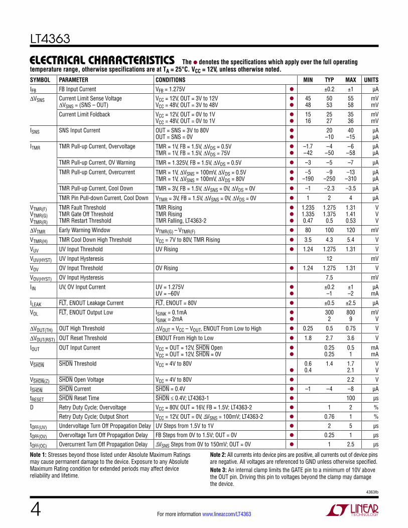
elecTrical characTerisTics The l denotes the specifications which apply over the full operating temperature range, otherwise specifications are at TA = 25°C. VCC = 12V, unless otherwise noted.SYMBOL PARAMETER CONDITIONS MIN TYP MAX UNITSVCC Operating Voltage Range LT4363 l 4 80 VICC VCC Supply Current SHDN Open, OUT = SNS = 12V
SHDN = 0V, OUT = SNS = 0Vl
l
0.7 7
1.2 20 40
mA µA µA
IR Reverse Input Current VCC = –60V, SHDN, UV, OV Open VCC = SHDN = UV = OV = –60V
l
l
–0.5 –3
–4 –10
mA mA
ΔVGATE GATE Drive ΔVGATE = (GATE – SNS);VCC = OUT VCC = 4V; IGATE = –0.5µA, 0µA 9V ≤ VCC ≤ 80V; IGATE = –1µA, 0µA
l
l
4.5 10
13
16
V V
IGATE(UP) GATE Pull-Up Current VCC = GATE = OUT = 12V VCC = GATE = OUT = 48V
l
l
–15 –20
–30 –40
–45 –65
µA µA
IGATE(DN) GATE Pull-Down Current Overvoltage: FB = 1.5V, GATE = 12V, OUT = 5V Overcurrent: ΔVSNS = 150mV, VGATE = 10V, OUT = 0V Shutdown/UV Mode: SHDN = 0V, GATE = 10V UV = 1V, GATE = 10V
l
l
l
l
75 50 50
200
150 100
1000 1000
mA mA µA µA
VFB FB Servo Voltage GATE = 12V; OUT = 8V l 1.25 1.275 1.3 V
LT4363
44363fb
For more information www.linear.com/LT4363
Note 2: All currents into device pins are positive, all currents out of device pins are negative. All voltages are referenced to GND unless otherwise specified.Note 3: An internal clamp limits the GATE pin to a minimum of 10V above the OUT pin. Driving this pin to voltages beyond the clamp may damage the device.
SYMBOL PARAMETER CONDITIONS MIN TYP MAX UNITSIFB FB Input Current VFB = 1.275V l ±0.2 ±1 µA
ΔVSNS Current Limit Sense Voltage ΔVSNS = (SNS – OUT)
VCC = 12V, OUT = 3V to 12V VCC = 48V, OUT = 3V to 48V
l
l
45 48
50 53
55 58
mV mV
Current Limit Foldback VCC = 12V, OUT = 0V to 1V VCC = 48V, OUT = 0V to 1V
l
l
15 16
25 27
35 36
mV mV
ISNS SNS Input Current OUT = SNS = 3V to 80V OUT = SNS = 0V
l
l
20 –10
40 –15
µA µA
ITMR TMR Pull-up Current, Overvoltage TMR = 1V, FB = 1.5V, ΔVDS = 0.5V TMR = 1V, FB = 1.5V, ΔVDS = 75V
l
l
–1.7 –42
–4 –50
–6 –58
µA µA
TMR Pull-up Current, OV Warning TMR = 1.325V, FB = 1.5V, ΔVDS = 0.5V l –3 –5 –7 µA
TMR Pull-up Current, Overcurrent TMR = 1V, ΔVSNS = 100mV, ΔVDS = 0.5V TMR = 1V, ΔVSNS = 100mV, ΔVDS = 80V
l
l
–5 –190
–9 –250
–13 –310
µA µA
TMR Pull-up Current, Cool Down TMR = 3V, FB = 1.5V, ΔVSNS = 0V, ΔVDS = 0V l –1 –2.3 –3.5 µA
TMR Pin Pull-down Current, Cool Down VTMR = 3V, FB = 1.5V, ΔVSNS = 0V, ΔVDS = 0V l 1 2 4 µA
VTMR(F) VTMR(G) VTMR(R)
TMR Fault Threshold TMR Gate Off Threshold TMR Restart Threshold
TMR Rising TMR Rising TMR Falling, LT4363-2
l
l
l
1.235 1.335 0.47
1.275 1.375 0.5
1.31 1.41 0.53
V V V
ΔVTMR Early Warning Window VTMR(G) – VTMR(F) l 80 100 120 mV
VTMR(H) TMR Cool Down High Threshold VCC = 7V to 80V, TMR Rising l 3.5 4.3 5.4 V
VUV UV Input Threshold UV Rising l 1.24 1.275 1.31 V
VUV(HYST) UV Input Hysteresis 12 mV
VOV OV Input Threshold OV Rising l 1.24 1.275 1.31 V
VOV(HYST) OV Input Hysteresis 7.5 mV
IIN UV, OV Input Current UV = 1.275V UV = –60V
l
l
±0.2 –1
±1 –2
µA mA
ILEAK FLT, ENOUT Leakage Current FLT, ENOUT = 80V l ±0.5 ±2.5 µA
VOL FLT, ENOUT Output Low ISINK = 0.1mA ISINK = 2mA
l
l
300 2
800 9
mV V
ΔVOUT(TH) OUT High Threshold ΔVOUT = VCC – VOUT, ENOUT From Low to High l 0.25 0.5 0.75 V
ΔVOUT(RST) OUT Reset Threshold ENOUT From High to Low l 1.8 2.7 3.6 V
IOUT OUT Input Current VCC = OUT = 12V, SHDN Open VCC = OUT = 12V, SHDN = 0V
l
l
0.25 0.25
0.5 1
mA mA
VSHDN SHDN Threshold VCC = 4V to 80V
l
0.6 0.4
1.4 1.7 2.1
V V
VSHDN(Z) SHDN Open Voltage VCC = 4V to 80V l 2.2 VISHDN SHDN Current SHDN = 0.4V l –1 –4 –8 µAtRESET SHDN Reset Time SHDN ≤ 0.4V; LT4363-1 l 100 µsD Retry Duty Cycle; Overvoltage VCC = 80V, OUT = 16V, FB = 1.5V; LT4363-2 l 1 2 %
Retry Duty Cycle; Output Short VCC = 12V, OUT = 0V, ∆VSNS = 100mV; LT4363-2 l 0.76 1 %tOFF(UV) Undervoltage Turn Off Propagation Delay UV Steps from 1.5V to 1V l 2 5 µstOFF(OV) Overvoltage Turn Off Propagation Delay FB Steps from 0V to 1.5V; OUT = 0V l 0.25 1 µstOFF(OC) Overcurrent Turn Off Propagation Delay ∆VSNS Steps from 0V to 150mV; OUT = 0V l 1 2.5 µs
Note 1: Stresses beyond those listed under Absolute Maximum Ratings may cause permanent damage to the device. Exposure to any Absolute Maximum Rating condition for extended periods may affect device reliability and lifetime.
elecTrical characTerisTics The l denotes the specifications which apply over the full operating temperature range, otherwise specifications are at TA = 25°C. VCC = 12V, unless otherwise noted.
LT4363
54363fb
For more information www.linear.com/LT4363
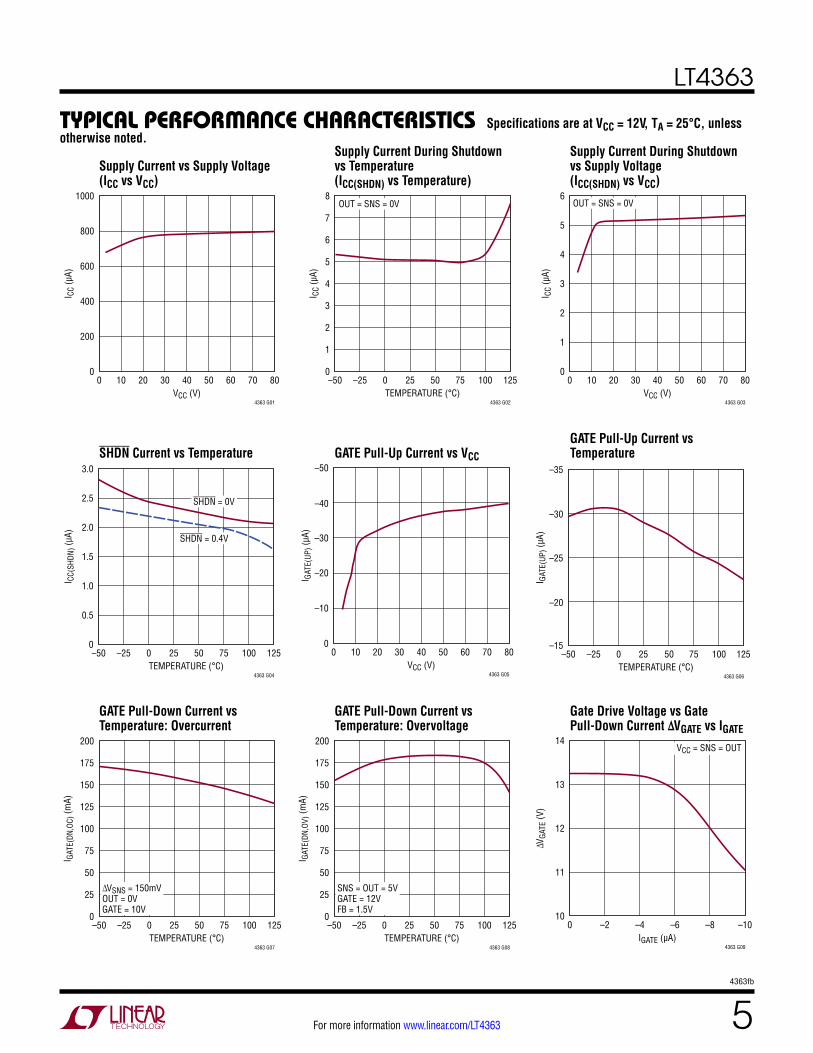
Specifications are at VCC = 12V, TA = 25°C, unless otherwise noted.Typical perForMance characTerisTics
SHDN Current vs Temperature GATE Pull-Up Current vs VCC
GATE Pull-Up Current vs Temperature
GATE Pull-Down Current vs Temperature: Overcurrent
GATE Pull-Down Current vs Temperature: Overvoltage
Gate Drive Voltage vs Gate Pull-Down Current ΔVGATE vs IGATE
Supply Current vs Supply Voltage (ICC vs VCC)
Supply Current During Shutdown vs Temperature (ICC(SHDN) vs Temperature)
Supply Current During Shutdown vs Supply Voltage (ICC(SHDN) vs VCC)
VCC (V)0
I CC
(µA)
1000
800
600
400
200
0
4363 G01
8070605020 4010 30VCC (V)
0
I CC
(µA)
6
5
4
3
2
1
0
4363 G03
8070605020 4010 30
OUT = SNS = 0V
TEMPERATURE (°C)–50
I CC
(µA)
8
7
5
6
4
2
3
1
00 50–25 25 100
4363 G02
12575
OUT = SNS = 0V
TEMPERATURE (°C)–50
I CC(
SHDN
) (µA
)
3.0
2.5
1.5
2.0
0.5
1.0
00 50–25 25 100
4363 G04
12575
SHDN = 0V
SHDN = 0.4V
TEMPERATURE (°C)–50 0 50–25 25 100 12575
I GAT
E(DN
,OC)
(mA)
200
125
100
175
150
75
50
25
0
4363 G07
∆VSNS = 150mVOUT = 0VGATE = 10V
TEMPERATURE (°C)–50 0 50–25 25 100 12575
I GAT
E(DN
,OV)
(mA)
200
125
100
175
150
75
50
25
0
4363 G08
SNS = OUT = 5VGATE = 12VFB = 1.5V
VCC (V)0
I GAT
E(UP
) (µA
)
–50
–30
–40
–20
–10
0
4363 G05
8070605020 4010 30
IGATE (µA)0
∆VGA
TE (V
)
14
13
12
11
10–6
4363 G09
–10–8–4–2
VCC = SNS = OUT
TEMPERATURE (°C)–50 0 50–25 25 10075 125
I GAT
E(UP
) (µA
)
–30
–35
–25
–20
–15
4363 G06
LT4363
64363fb
For more information www.linear.com/LT4363
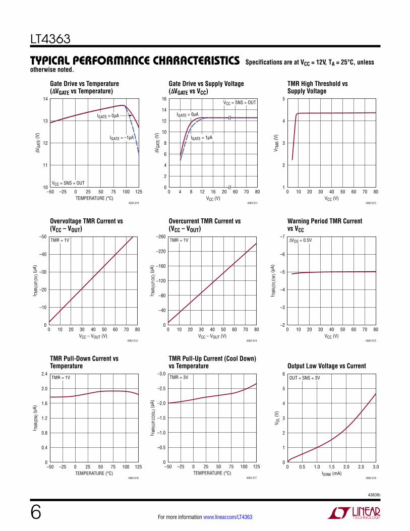
Typical perForMance characTerisTics
Overvoltage TMR Current vs (VCC – VOUT)
Overcurrent TMR Current vs (VCC – VOUT)
Warning Period TMR Current vs VCC
TMR Pull-Down Current vs Temperature
TMR Pull-Up Current (Cool Down) vs Temperature Output Low Voltage vs Current
Gate Drive vs Temperature (ΔVGATE vs Temperature)
Gate Drive vs Supply Voltage (ΔVGATE vs VCC)
TMR High Threshold vs Supply Voltage
Specifications are at VCC = 12V, TA = 25°C, unless otherwise noted.
TEMPERATURE (°C)–50
∆VGA
TE (V
)
14
13
11
12
100 50–25 25 100
4363 G10
12575
VCC = SNS = OUT
IGATE = –1µA
IGATE = 0µA
VCC (V)0
∆VGA
TE (V
)
16
10
8
14
12
6
4
2
0
4363 G11
807060208 164 12
VCC = SNS = OUT
IGATE = 0µA
IGATE = 1µA
VCC (V)0
V TM
R (V
)
5
4
3
2
1
4363 G12
8070605020 4010 30
TEMPERATURE (°C)–50
I TM
R(DN
) (µA
)
2.4
2.0
1.2
1.6
0.4
0.8
00 50–25 25 100
4363 G16
12575
TMR = 1V
ISINK (mA)0
V OL
(V)
6
5
4
3
2
1
0
4363 G18
3.02.52.01.51.00.5
OUT = SNS = 3V
VCC – VOUT (V)0
I TM
R(U
P,O
V) (µ
A)
–50
–40
–30
–20
–10
0
4363 G13
8070605020 4010 30
TMR = 1V
VCC (V)0
I TM
R(O
V,EW
) (µA
)
–7
–6
–5
–4
–3
–2
4363 G15
8070605020 4010 30
∆VDS = 0.5V
TEMPERATURE (°C)–50
I TM
R(U
P,CO
OL)
(µA)
–3.0
–2.5
–1.5
–2.0
–0.5
–1.0
00 50–25 25 100
4363 G17
12575
TMR = 3V
VCC – VOUT (V)0
I TM
R(U
P,O
C) (µ
A)
–260
–220
–160
–120
–80
–40
0
4363 G14
8070605020 4010 30
TMR = 1V
LT4363
74363fb
For more information www.linear.com/LT4363
Typical perForMance characTerisTics
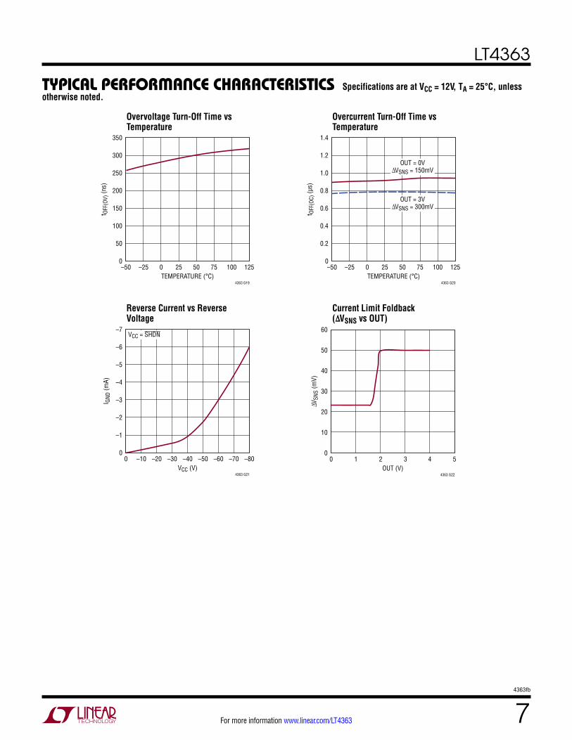
Reverse Current vs Reverse Voltage
Current Limit Foldback (ΔVSNS vs OUT)
Overvoltage Turn-Off Time vs Temperature
Overcurrent Turn-Off Time vs Temperature
Specifications are at VCC = 12V, TA = 25°C, unless otherwise noted.
TEMPERATURE (°C)–50 0 50–25 25 100 12575
t OFF
(OV)
(ns)
350
200
100
300
150
250
50
0
4363 G19TEMPERATURE (°C)
–50 0 50–25 25 100 12575
t OFF
(OC)
(µs)
1.4
0.8
0.4
1.2
0.6
1.0
0.2
0
4363 G20
OUT = 0V∆VSNS = 150mV
OUT = 3V∆VSNS = 300mV
VCC (V)0
I GND
(mA)
–7
–4
–3
–6
–5
–2
–1
0
4363 G21
–80–70–60–50–20 –40–10 –30
VCC = SHDN
OUT (V)0
∆VSN
S (m
V)
60
40
20
0
50
30
10
4363 G22
5431 2
LT4363
84363fb
For more information www.linear.com/LT4363
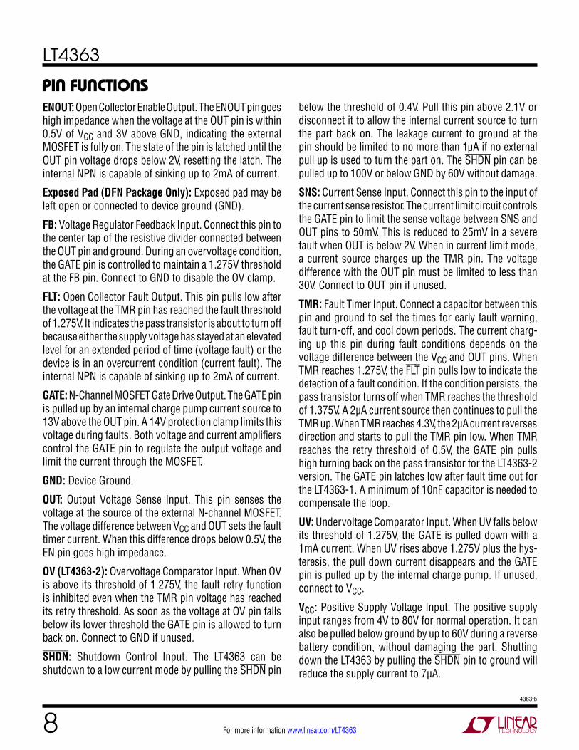
pin FuncTionsENOUT: Open Collector Enable Output. The ENOUT pin goes high impedance when the voltage at the OUT pin is within 0.5V of VCC and 3V above GND, indicating the external MOSFET is fully on. The state of the pin is latched until the OUT pin voltage drops below 2V, resetting the latch. The internal NPN is capable of sinking up to 2mA of current.
Exposed Pad (DFN Package Only): Exposed pad may be left open or connected to device ground (GND).
FB: Voltage Regulator Feedback Input. Connect this pin to the center tap of the resistive divider connected between the OUT pin and ground. During an overvoltage condition, the GATE pin is controlled to maintain a 1.275V threshold at the FB pin. Connect to GND to disable the OV clamp.
FLT: Open Collector Fault Output. This pin pulls low after the voltage at the TMR pin has reached the fault threshold of 1.275V. It indicates the pass transistor is about to turn off because either the supply voltage has stayed at an elevated level for an extended period of time (voltage fault) or the device is in an overcurrent condition (current fault). The internal NPN is capable of sinking up to 2mA of current.
GATE: N-Channel MOSFET Gate Drive Output. The GATE pin is pulled up by an internal charge pump current source to 13V above the OUT pin. A 14V protection clamp limits this voltage during faults. Both voltage and current amplifiers control the GATE pin to regulate the output voltage and limit the current through the MOSFET.
GND: Device Ground.
OUT: Output Voltage Sense Input. This pin senses the voltage at the source of the external N-channel MOSFET. The voltage difference between VCC and OUT sets the fault timer current. When this difference drops below 0.5V, the EN pin goes high impedance.
OV (LT4363-2): Overvoltage Comparator Input. When OV is above its threshold of 1.275V, the fault retry function is inhibited even when the TMR pin voltage has reached its retry threshold. As soon as the voltage at OV pin falls below its lower threshold the GATE pin is allowed to turn back on. Connect to GND if unused.
SHDN: Shutdown Control Input. The LT4363 can be shutdown to a low current mode by pulling the SHDN pin
below the threshold of 0.4V. Pull this pin above 2.1V or disconnect it to allow the internal current source to turn the part back on. The leakage current to ground at the pin should be limited to no more than 1µA if no external pull up is used to turn the part on. The SHDN pin can be pulled up to 100V or below GND by 60V without damage.
SNS: Current Sense Input. Connect this pin to the input of the current sense resistor. The current limit circuit controls the GATE pin to limit the sense voltage between SNS and OUT pins to 50mV. This is reduced to 25mV in a severe fault when OUT is below 2V. When in current limit mode, a current source charges up the TMR pin. The voltage difference with the OUT pin must be limited to less than 30V. Connect to OUT pin if unused.
TMR: Fault Timer Input. Connect a capacitor between this pin and ground to set the times for early fault warning, fault turn-off, and cool down periods. The current charg-ing up this pin during fault conditions depends on the voltage difference between the VCC and OUT pins. When TMR reaches 1.275V, the FLT pin pulls low to indicate the detection of a fault condition. If the condition persists, the pass transistor turns off when TMR reaches the threshold of 1.375V. A 2µA current source then continues to pull the TMR up. When TMR reaches 4.3V, the 2µA current reverses direction and starts to pull the TMR pin low. When TMR reaches the retry threshold of 0.5V, the GATE pin pulls high turning back on the pass transistor for the LT4363-2 version. The GATE pin latches low after fault time out for the LT4363-1. A minimum of 10nF capacitor is needed to compensate the loop.
UV: Undervoltage Comparator Input. When UV falls below its threshold of 1.275V, the GATE is pulled down with a 1mA current. When UV rises above 1.275V plus the hys-teresis, the pull down current disappears and the GATE pin is pulled up by the internal charge pump. If unused, connect to VCC.
VCC: Positive Supply Voltage Input. The positive supply input ranges from 4V to 80V for normal operation. It can also be pulled below ground by up to 60V during a reverse battery condition, without damaging the part. Shutting down the LT4363 by pulling the SHDN pin to ground will reduce the supply current to 7µA.
LT4363
94363fb
For more information www.linear.com/LT4363
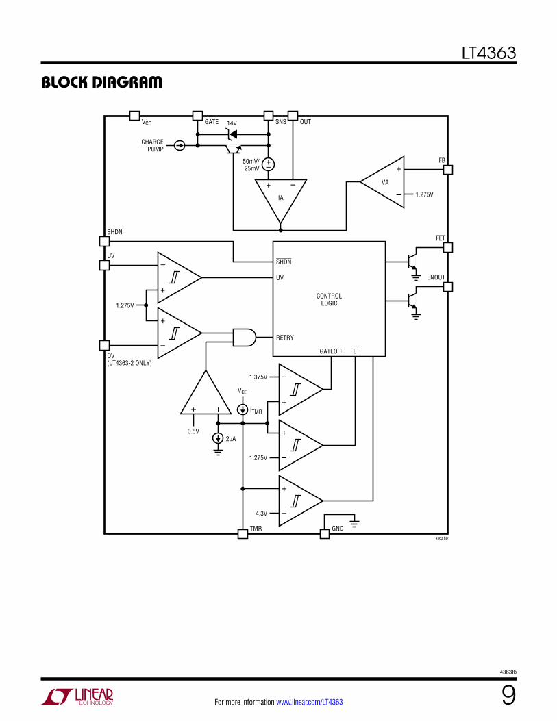
block DiagraM
+ –
+–
SNSVCC
SHDN
OV (LT4363-2 ONLY)
IA
50mV/25mV
2µA
1.375V
14V
1.275V
1.275V
4.3V
1.275V
–+
0.5V
OUT
TMR GND
GATE
UV
4363 BD
VCC
ITMR
FLT
ENOUT
FB+
–
CHARGEPUMP
CONTROLLOGIC
GATEOFF FLT
VA
SHDN
RETRY
UV
+
–
–
+
+
–
–
+
–
+
LT4363
104363fb
For more information www.linear.com/LT4363
operaTionSome power systems must cope with high voltage surges of short duration such as those in vehicles. Load circuitry must be protected from these transients, yet high availability systems must continue operating during these events.
The LT4363 is an overvoltage protection regulator that drives an external N-channel MOSFET as the pass transis-tor. It operates from a wide supply voltage range of 4V to 80V. It can also be pulled below ground potential by up to 60V without damage. The low power supply require-ment of 4V allows it to operate even during cold cranking conditions in automotive applications. The internal charge pump turns on the N-channel MOSFET to supply current to the loads with very little power loss. Two MOSFETs can be connected back to back to replace an inline Schottky diode for reverse input protection. This improves the ef-ficiency and increases the available supply voltage level to the load circuitry during cold crank.
Normally, the pass transistor is fully on, powering the loads with very little voltage drop. When the supply voltage surges too high, the voltage amplifier (VA) controls the gate of the MOSFET and regulates the voltage at the OUT pin to a level that is set by the external resistive divider from the OUT pin to ground and the internal 1.275V reference. A current source starts charging up the capacitor connected at the TMR pin to ground. If the TMR voltage reaches 1.275V, the FLT pin pulls low to indicate impending turn-off due to the overvoltage condition. The pass transistor stays on until TMR reaches 1.375V, at which point the GATE pin pulls low turning off the MOSFET.
A current continues to pull the TMR pin up until it reaches about 4.3V, at which point the current reverses direction and pulls the TMR pin down. For the LT4363-2 version, when the voltage at the TMR pin reaches 0.5V the GATE pin begins rising, turning on the MOSFET. The FLT pin will then return to a high impedance state. For the latch-off version, LT4363-1, both the GATE and FLT pins remain low even after TMR has reached the 0.5V threshold. Allow
sufficient time for TMR to discharge to 0.5V and for the MOSFET to cool before attempting to reset the part. To reset, pull the SHDN pin low for at least 100µs, then pull high with a slew rate of at least 10V/ms.
The fault timer allows the load to continue functioning during short transient events while protecting the MOSFET from being damaged by a long period of supply overvolt-age, such as a load dump in vehicles. The timer period varies with the voltage across the MOSFET. A higher volt-age corresponds to a shorter fault timer period, helping to keep the MOSFET within its safe operating area (SOA).
The LT4363 senses an overcurrent condition by monitor-ing the voltage across an optional sense resistor placed between the SNS and OUT pins. An active current limit circuit (IA) controls the GATE pin to limit the sense volt-age to 50mV, if the OUT pin potential is above 2V. In the case of a severe output short that brings OUT below 2V, the servo sense voltage is reduced to 25mV to reduce the stress on the pass transistor. During current limit, the current charging the TMR capacitor is about 5 times the current during an overvoltage event. The FLT pin pulls low when the TMR voltage reaches 1.275V and the MOSFET is turned off when it reaches 1.375V. The MOSFET turns back on and the FLT pin returns to a high impedance state after TMR has reached the 0.5V threshold for the LT4363-2 version. For the latch-off version, LT4363-1, both the GATE and FLT pins remain low even after TMR has reached the 0.5V threshold. Reset the part in the same way as in overvoltage time-out case.
An accurate undervoltage comparator keeps the GATE pin low until the voltage at the UV pin is above the 1.275V threshold. An overvoltage comparator prevents the MOSFET from turning on after fault time-out while the voltage at the OV pin is still above 1.275V for the LT4363-2. The SHDN pin turns off the pass transistor and all the internal circuitry, reducing the supply current to a mere 7µA.
LT4363
114363fb
For more information www.linear.com/LT4363
applicaTions inForMaTionThe LT4363 limits the voltage and current delivered to the load during supply transient or output overload events. The total fault timer period is set to ride through short-duration faults, while longer events cause the output to shut off and protect the MOSFET pass device from damage. The MOSFET provides a low resistance path from the input to the load during normal operation, while in fault conditions it operates as a series regulator.
Overvoltage Fault
The LT4363 limits the voltage at the output during an overvoltage at the input. An internal amplifier regulates the GATE pin to maintain 1.275V at the FB pin. During this interval the MOSFET is on and supplies current to the load. This allows uninterrupted operation during short overvoltage events. If the overvoltage condition persists, the timer causes the MOSFET to turn off.
Overcurrent Fault
The LT4363 features and adjustable current limit that pro-tects against output short circuits or excessive load current. During an overcurrent event, the GATE pin is regulated to limit the current sense voltage across the SNS and OUT pins to 50mV. In the case of a severe short at the output, where OUT is less than 2V, the current sense voltage is reduced to 25mV to further reduce power dissipation in the MOSFET. If the overcurrent condition persists, the timer causes the MOSFET to turn off.
Fault Timer Overview
Overvoltage and overcurrent conditions are limited in duration by an adjustable timer. A capacitor at the TMR pin sets the delay time before a fault condition is reported at the FLT pin as well as the overall delay before the MOSFET is turned off. The same capacitor also sets the cool down time before the MOSFET is allowed to turn back on.
When either an overvoltage or overcurrent fault condition occurs, a current source charges the TMR pin capacitor. The exact current level varies as a function of the type of fault and the VDS voltage drop across the MOSFET. This scheme takes better advantage of the MOSFET’s available Safe Operating Area (SOA) than would a fixed timer current.
The TMR pin is biased to 0.5V under normal operating
conditions. In the presence of a fault the timer first charges to 1.275V, and then enters the early warning phase of operation. At this point the FLT pin pulls low and after charging to 1.375V, the timer shuts off the MOSFET. The warning phase is indicated by FLT low and gives time for the load to perform house-keeping chores such as data storage in anticipation of impending power loss. After faulting off, the timer enters the cool down phase. At the end of the cool down period the LT4363-1 remains off until reset, while the LT4363-2 automatically restarts. For the LT4363-2 retry is inhibited if the OV pin is greater than 1.275V. This prevents motorboating in the event there is a sustained input overvoltage condition.
Fault Timer Operation in Overvoltage
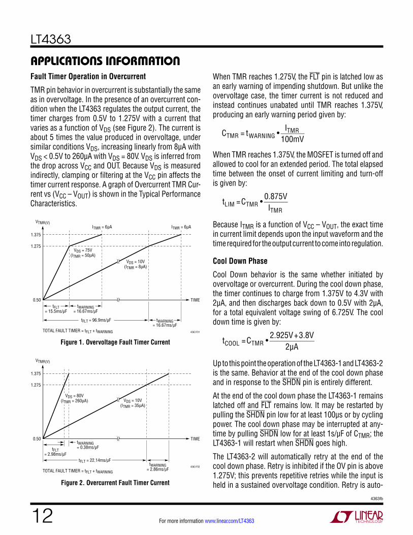
In the presence of an overvoltage condition when the LT4363 regulates the output voltage, the timer charges from 0.5V to 1.275V with a current that varies as a func-tion of VDS (see Figure 1). VDS is inferred from the drop across VCC and OUT. The timer current increases linearly from around 4µA with VDS ≤ 0.5V, to 50µA with VDS = 75V. Because VDS is measured indirectly, clamping or filtering at the VCC pin affects the timer current response. A graph of Overvoltage TMR Current vs (VCC – VOUT) is shown in the Typical Performance Characteristics.
When TMR reaches 1.275V, the FLT pin is latched low as an early warning of impending shutdown. The timer cur-rent is cut to a fixed value of 6µA and continues to run until TMR reaches 1.375V, producing a fixed early warning period given by:
CTMR = tWARNING •
6µA100mV
When TMR reaches 1.375V, the MOSFET is turned off and allowed to cool for an extended period. The total elapsed time between the onset of output regulation and turn-off is given by:
tREG =CTMR • 0.775V
ITMR+ 100mV
6µA
Because ITMR is a function of VCC – VOUT, the exact time in regulation depends upon the input waveform and the time required for the output voltage to come into regulation.
LT4363
124363fb
For more information www.linear.com/LT4363
tFLT= 15.5ms/µF
TOTAL FAULT TIMER = tFLT + tWARNING
tWARNING= 16.67ms/µF
tFLT = 96.9ms/µF tWARNING= 16.67ms/µF
VTMR(V)ITMR = 6µA ITMR = 6µA
VDS = 75V(ITMR = 50µA)
VDS = 10V(ITMR = 8µA)
1.375
1.275
TIME
4363 F01
0.50
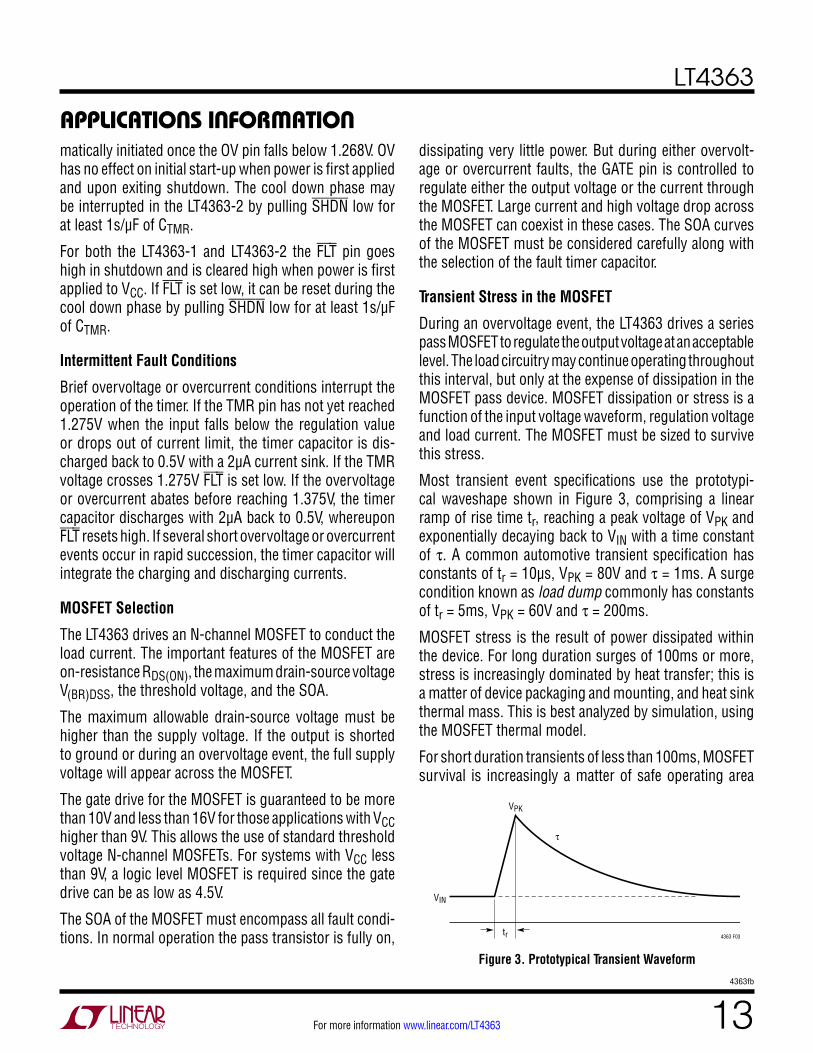
Fault Timer Operation in Overcurrent
TMR pin behavior in overcurrent is substantially the same as in overvoltage. In the presence of an overcurrent con-dition when the LT4363 regulates the output current, the timer charges from 0.5V to 1.275V with a current that varies as a function of VDS (see Figure 2). The current is about 5 times the value produced in overvoltage, under similar conditions VDS, increasing linearly from 8µA with VDS < 0.5V to 260µA with VDS = 80V. VDS is inferred from the drop across VCC and OUT. Because VDS is measured indirectly, clamping or filtering at the VCC pin affects the timer current response. A graph of Overcurrent TMR Cur-rent vs (VCC – VOUT) is shown in the Typical Performance Characteristics.
When TMR reaches 1.275V, the FLT pin is latched low as an early warning of impending shutdown. But unlike the overvoltage case, the timer current is not reduced and instead continues unabated until TMR reaches 1.375V, producing an early warning period given by:
CTMR = tWARNING •
ITMR100mV
When TMR reaches 1.375V, the MOSFET is turned off and allowed to cool for an extended period. The total elapsed time between the onset of current limiting and turn-off is given by:
tLIM =CTMR •
0.875VITMR
Because ITMR is a function of VCC – VOUT, the exact time in current limit depends upon the input waveform and the time required for the output current to come into regulation.
Cool Down Phase
Cool Down behavior is the same whether initiated by overvoltage or overcurrent. During the cool down phase, the timer continues to charge from 1.375V to 4.3V with 2µA, and then discharges back down to 0.5V with 2µA, for a total equivalent voltage swing of 6.725V. The cool down time is given by:
tCOOL =CTMR •
2.925V+3.8V2µA
Up to this point the operation of the LT4363-1 and LT4363-2 is the same. Behavior at the end of the cool down phase and in response to the SHDN pin is entirely different.
At the end of the cool down phase the LT4363-1 remains latched off and FLT remains low. It may be restarted by pulling the SHDN pin low for at least 100µs or by cycling power. The cool down phase may be interrupted at any-time by pulling SHDN low for at least 1s/µF of CTMR; the LT4363-1 will restart when SHDN goes high.
The LT4363-2 will automatically retry at the end of the cool down phase. Retry is inhibited if the OV pin is above 1.275V; this prevents repetitive retries while the input is held in a sustained overvoltage condition. Retry is auto-
applicaTions inForMaTion
Figure 1. Overvoltage Fault Timer Current
Figure 2. Overcurrent Fault Timer Current
tFLT= 2.98ms/µF
TOTAL FAULT TIMER = tFLT + tWARNING
tFLT = 22.14ms/µFtWARNING
= 2.86ms/µF
tWARNING = 0.38ms/µF
VTMR(V)
VDS = 10V(ITMR = 35µA)
1.375
1.275
0.50 TIME
4363 F02
VDS = 80V(ITMR = 260µA)
LT4363
134363fb
For more information www.linear.com/LT4363
applicaTions inForMaTionmatically initiated once the OV pin falls below 1.268V. OV has no effect on initial start-up when power is first applied and upon exiting shutdown. The cool down phase may be interrupted in the LT4363-2 by pulling SHDN low for at least 1s/µF of CTMR.
For both the LT4363-1 and LT4363-2 the FLT pin goes high in shutdown and is cleared high when power is first applied to VCC. If FLT is set low, it can be reset during the cool down phase by pulling SHDN low for at least 1s/µF of CTMR.
Intermittent Fault Conditions
Brief overvoltage or overcurrent conditions interrupt the operation of the timer. If the TMR pin has not yet reached 1.275V when the input falls below the regulation value or drops out of current limit, the timer capacitor is dis-charged back to 0.5V with a 2µA current sink. If the TMR voltage crosses 1.275V FLT is set low. If the overvoltage or overcurrent abates before reaching 1.375V, the timer capacitor discharges with 2µA back to 0.5V, whereupon FLT resets high. If several short overvoltage or overcurrent events occur in rapid succession, the timer capacitor will integrate the charging and discharging currents.
MOSFET Selection
The LT4363 drives an N-channel MOSFET to conduct the load current. The important features of the MOSFET are on-resistance RDS(ON), the maximum drain-source voltage V(BR)DSS, the threshold voltage, and the SOA.
The maximum allowable drain-source voltage must be higher than the supply voltage. If the output is shorted to ground or during an overvoltage event, the full supply voltage will appear across the MOSFET.
The gate drive for the MOSFET is guaranteed to be more than 10V and less than 16V for those applications with VCC higher than 9V. This allows the use of standard threshold voltage N-channel MOSFETs. For systems with VCC less than 9V, a logic level MOSFET is required since the gate drive can be as low as 4.5V.
The SOA of the MOSFET must encompass all fault condi-tions. In normal operation the pass transistor is fully on,
dissipating very little power. But during either overvolt-age or overcurrent faults, the GATE pin is controlled to regulate either the output voltage or the current through the MOSFET. Large current and high voltage drop across the MOSFET can coexist in these cases. The SOA curves of the MOSFET must be considered carefully along with the selection of the fault timer capacitor.
Transient Stress in the MOSFET
During an overvoltage event, the LT4363 drives a series pass MOSFET to regulate the output voltage at an acceptable level. The load circuitry may continue operating throughout this interval, but only at the expense of dissipation in the MOSFET pass device. MOSFET dissipation or stress is a function of the input voltage waveform, regulation voltage and load current. The MOSFET must be sized to survive this stress.
Most transient event specifications use the prototypi-cal waveshape shown in Figure 3, comprising a linear ramp of rise time tr, reaching a peak voltage of VPK and exponentially decaying back to VIN with a time constant of τ. A common automotive transient specification has constants of tr = 10µs, VPK = 80V and τ = 1ms. A surge condition known as load dump commonly has constants of tr = 5ms, VPK = 60V and τ = 200ms.
MOSFET stress is the result of power dissipated within the device. For long duration surges of 100ms or more, stress is increasingly dominated by heat transfer; this is a matter of device packaging and mounting, and heat sink thermal mass. This is best analyzed by simulation, using the MOSFET thermal model.
For short duration transients of less than 100ms, MOSFET survival is increasingly a matter of safe operating area
Figure 3. Prototypical Transient Waveform
VPK
τ
VIN
4363 F03tr
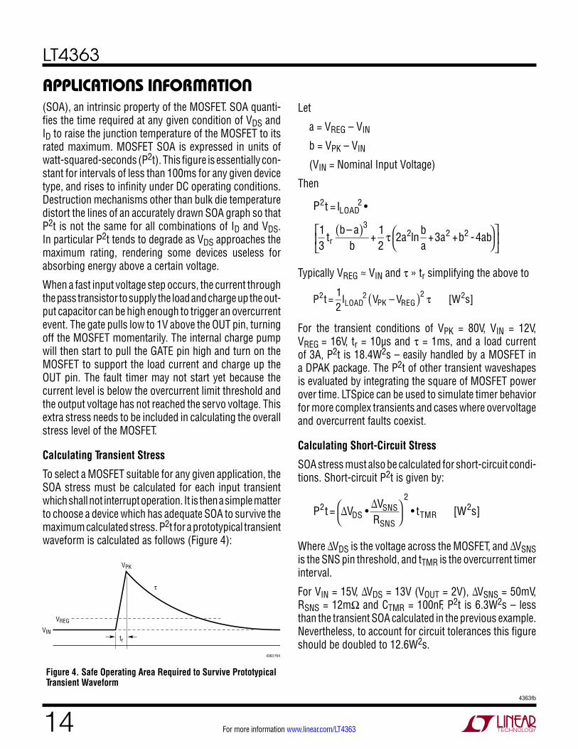
LT4363
144363fb
For more information www.linear.com/LT4363
(SOA), an intrinsic property of the MOSFET. SOA quanti-fies the time required at any given condition of VDS and ID to raise the junction temperature of the MOSFET to its rated maximum. MOSFET SOA is expressed in units of watt-squared-seconds (P2t). This figure is essentially con-stant for intervals of less than 100ms for any given device type, and rises to infinity under DC operating conditions. Destruction mechanisms other than bulk die temperature distort the lines of an accurately drawn SOA graph so that P2t is not the same for all combinations of ID and VDS. In particular P2t tends to degrade as VDS approaches the maximum rating, rendering some devices useless for absorbing energy above a certain voltage.
When a fast input voltage step occurs, the current through the pass transistor to supply the load and charge up the out-put capacitor can be high enough to trigger an overcurrent event. The gate pulls low to 1V above the OUT pin, turning off the MOSFET momentarily. The internal charge pump will then start to pull the GATE pin high and turn on the MOSFET to support the load current and charge up the OUT pin. The fault timer may not start yet because the current level is below the overcurrent limit threshold and the output voltage has not reached the servo voltage. This extra stress needs to be included in calculating the overall stress level of the MOSFET.
Calculating Transient Stress
To select a MOSFET suitable for any given application, the SOA stress must be calculated for each input transient which shall not interrupt operation. It is then a simple matter to choose a device which has adequate SOA to survive the maximum calculated stress. P2t for a prototypical transient waveform is calculated as follows (Figure 4):
Let
a = VREG – VIN
b = VPK – VIN
(VIN = Nominal Input Voltage)
Then
P2t = ILOAD2 •
13
trb– a( )3
b+
12
τ 2a2lnba
+3a2 +b2 -4ab
Typically VREG ≈ VIN and τ » tr simplifying the above to
P2t =
12
ILOAD2 VPK – VREG( )2 τ [W2s]
For the transient conditions of VPK = 80V, VIN = 12V, VREG = 16V, tr = 10µs and τ = 1ms, and a load current of 3A, P2t is 18.4W2s – easily handled by a MOSFET in a DPAK package. The P2t of other transient waveshapes is evaluated by integrating the square of MOSFET power over time. LTSpice can be used to simulate timer behavior for more complex transients and cases where overvoltage and overcurrent faults coexist.
Calculating Short-Circuit Stress
SOA stress must also be calculated for short-circuit condi-tions. Short-circuit P2t is given by:
P2t = ∆VDS •
∆VSNSRSNS
2
• tTMR [W2s]
Where ∆VDS is the voltage across the MOSFET, and ∆VSNS is the SNS pin threshold, and tTMR is the overcurrent timer interval.
For VIN = 15V, ∆VDS = 13V (VOUT = 2V), ∆VSNS = 50mV, RSNS = 12mΩ and CTMR = 100nF, P2t is 6.3W2s – less than the transient SOA calculated in the previous example. Nevertheless, to account for circuit tolerances this figure should be doubled to 12.6W2s.
applicaTions inForMaTion
Figure 4. Safe Operating Area Required to Survive Prototypical Transient Waveform
VPK
τ
VIN
4363 F04
VREG
tr
LT4363
154363fb
For more information www.linear.com/LT4363
CTMR0.1µF
RSNS10mΩ
Q1IRLR2908
Q2IRLR2908VIN
12VVOUT12V, 3ACLAMPEDAT 16V
4363 F06
LT4363DE-2
GND TMR9 12
OUT2
SNS3
SHDN6
UV8
OV7
VCC5
FLT
ENOUT
FB
10
11
1
C147nF
D1*SMAJ58CA
R24.99k
R157.6k
GATE4
R710k
R51M
Q32N3904
D21N4148
R310Ω
R410Ω
*DIODES INC.
applicaTions inForMaTion
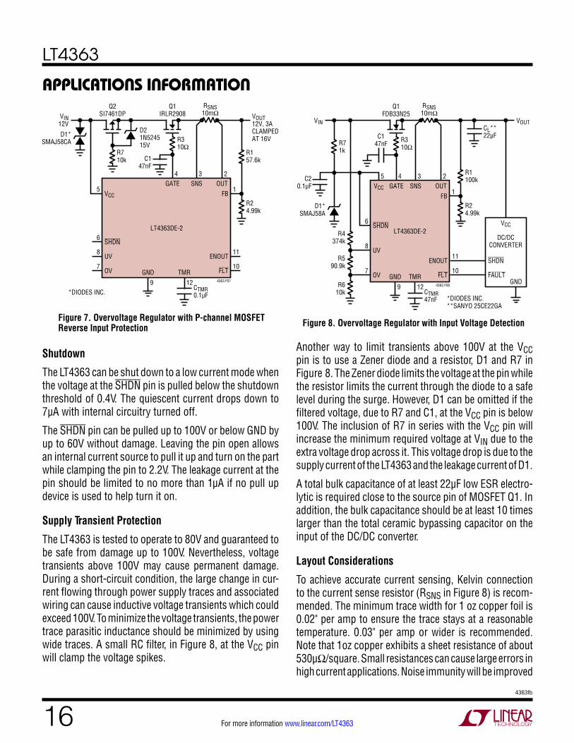
Figure 6. Overvoltage Regulator with N-channel MOSFET Reverse Input Protection
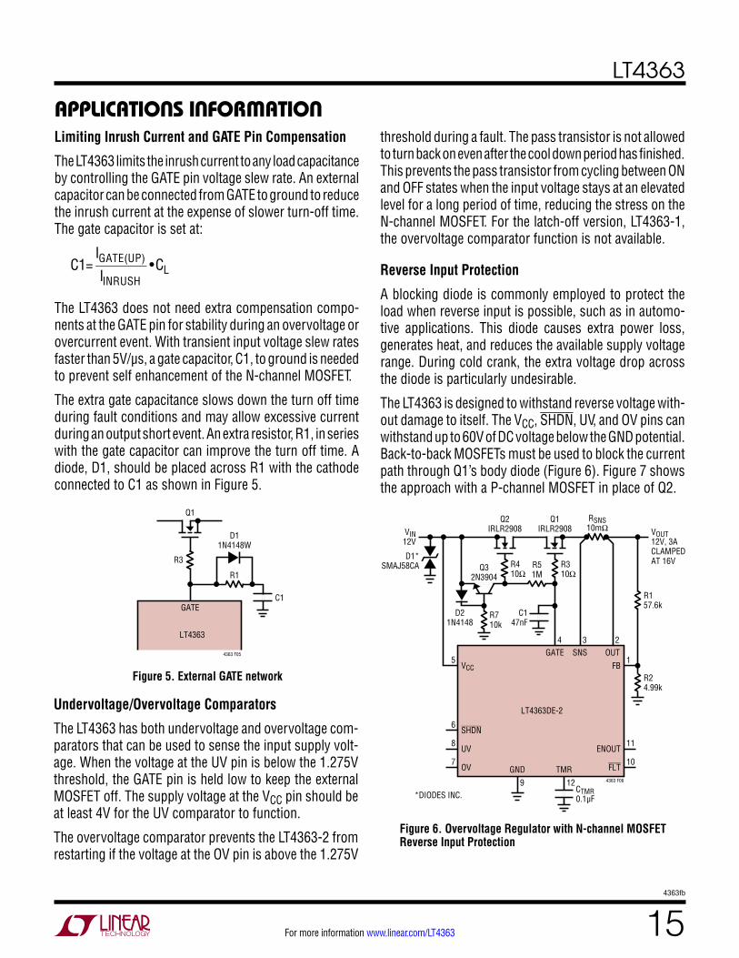
Figure 5. External GATE network
Limiting Inrush Current and GATE Pin Compensation
The LT4363 limits the inrush current to any load capacitance by controlling the GATE pin voltage slew rate. An external capacitor can be connected from GATE to ground to reduce the inrush current at the expense of slower turn-off time. The gate capacitor is set at:
C1=
IGATE(UP)
IINRUSH•CL
The LT4363 does not need extra compensation compo-nents at the GATE pin for stability during an overvoltage or overcurrent event. With transient input voltage slew rates faster than 5V/µs, a gate capacitor, C1, to ground is needed to prevent self enhancement of the N-channel MOSFET.
The extra gate capacitance slows down the turn off time during fault conditions and may allow excessive current during an output short event. An extra resistor, R1, in series with the gate capacitor can improve the turn off time. A diode, D1, should be placed across R1 with the cathode connected to C1 as shown in Figure 5.
threshold during a fault. The pass transistor is not allowed to turn back on even after the cool down period has finished. This prevents the pass transistor from cycling between ON and OFF states when the input voltage stays at an elevated level for a long period of time, reducing the stress on the N-channel MOSFET. For the latch-off version, LT4363-1, the overvoltage comparator function is not available.
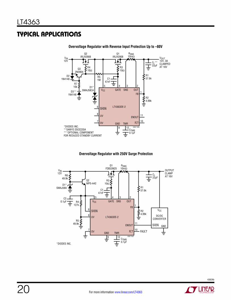
Reverse Input Protection
A blocking diode is commonly employed to protect the load when reverse input is possible, such as in automo-tive applications. This diode causes extra power loss, generates heat, and reduces the available supply voltage range. During cold crank, the extra voltage drop across the diode is particularly undesirable.
The LT4363 is designed to withstand reverse voltage with-out damage to itself. The VCC, SHDN, UV, and OV pins can withstand up to 60V of DC voltage below the GND potential. Back-to-back MOSFETs must be used to block the current path through Q1’s body diode (Figure 6). Figure 7 shows the approach with a P-channel MOSFET in place of Q2.
Undervoltage/Overvoltage Comparators
The LT4363 has both undervoltage and overvoltage com-parators that can be used to sense the input supply volt-age. When the voltage at the UV pin is below the 1.275V threshold, the GATE pin is held low to keep the external MOSFET off. The supply voltage at the VCC pin should be at least 4V for the UV comparator to function.
The overvoltage comparator prevents the LT4363-2 from restarting if the voltage at the OV pin is above the 1.275V
C1
R3
4363 F05
LT4363
GATE
Q1
R1
D11N4148W
LT4363
164363fb
For more information www.linear.com/LT4363
applicaTions inForMaTion
Shutdown
The LT4363 can be shut down to a low current mode when the voltage at the SHDN pin is pulled below the shutdown threshold of 0.4V. The quiescent current drops down to 7µA with internal circuitry turned off.
The SHDN pin can be pulled up to 100V or below GND by up to 60V without damage. Leaving the pin open allows an internal current source to pull it up and turn on the part while clamping the pin to 2.2V. The leakage current at the pin should be limited to no more than 1µA if no pull up device is used to help turn it on.
Supply Transient Protection
The LT4363 is tested to operate to 80V and guaranteed to be safe from damage up to 100V. Nevertheless, voltage transients above 100V may cause permanent damage. During a short-circuit condition, the large change in cur-rent flowing through power supply traces and associated wiring can cause inductive voltage transients which could exceed 100V. To minimize the voltage transients, the power trace parasitic inductance should be minimized by using wide traces. A small RC filter, in Figure 8, at the VCC pin will clamp the voltage spikes.
Another way to limit transients above 100V at the VCC pin is to use a Zener diode and a resistor, D1 and R7 in Figure 8. The Zener diode limits the voltage at the pin while the resistor limits the current through the diode to a safe level during the surge. However, D1 can be omitted if the filtered voltage, due to R7 and C1, at the VCC pin is below 100V. The inclusion of R7 in series with the VCC pin will increase the minimum required voltage at VIN due to the extra voltage drop across it. This voltage drop is due to the supply current of the LT4363 and the leakage current of D1.
A total bulk capacitance of at least 22µF low ESR electro-lytic is required close to the source pin of MOSFET Q1. In addition, the bulk capacitance should be at least 10 times larger than the total ceramic bypassing capacitor on the input of the DC/DC converter.
Layout Considerations
To achieve accurate current sensing, Kelvin connection to the current sense resistor (RSNS in Figure 8) is recom-mended. The minimum trace width for 1 oz copper foil is 0.02" per amp to ensure the trace stays at a reasonable temperature. 0.03" per amp or wider is recommended. Note that 1oz copper exhibits a sheet resistance of about 530µΩ/square. Small resistances can cause large errors in high current applications. Noise immunity will be improved
Figure 8. Overvoltage Regulator with Input Voltage Detection
CTMR47nF
RSNS10mΩ
Q1FDB33N25
VIN VOUT
4363 F08
LT4363DE-2
GND TMR9 12
OUT2
SNS3
FB1
C20.1µF
D1*SMAJ58A
R24.99k
R1100k
R71k
GATE4
VCC
5
R310Ω
*DIODES INC.**SANYO 25CE22GA
SHDN6
UV8
OV7
DC/DCCONVERTER
GND
SHDN
VCC
FLT
ENOUT10
11
CL**22µF
FAULT
R590.9k
R610k
R4374k
C147nF
CTMR0.1µF
RSNS10mΩ
Q1IRLR2908
Q2SI7461DPVIN
12VVOUT12V, 3ACLAMPEDAT 16V
4363 F07
LT4363DE-2
GND TMR9 12
OUT2
SNS3
VCC5
FB1
D1*SMAJ58CA
R24.99k
R157.6k
GATE4
R710k
D21N524515V
R310Ω
*DIODES INC.
SHDN6
UV8
OV7
FLT
ENOUT10
11
C147nF
Figure 7. Overvoltage Regulator with P-channel MOSFET Reverse Input Protection
LT4363
174363fb
For more information www.linear.com/LT4363
applicaTions inForMaTionsignificantly by locating resistive dividers close to the pins with short VCC and GND traces.
Design Example
As a design example, take an application with the follow-ing specifications: VCC = 8V to 14V DC with a transient of 150V and decay time constant (τ) of 400ms, VOUT ≤ 27V, current limit (ILIM) at 5A, low battery detection of 6V, input overvoltage level at 60V, and 1ms of overvoltage early warning (Figure 8).
Selection of SMAJ58A for D1 will limit the voltage at the VCC pin to less than 71V during 150V surge. The minimum required voltage at the VCC pin is 4V when VIN is at 8V; the supply current for LT4363 is 1.5mA. The maximum value for R7 to ensure proper operation is:
R7=
8V – 4V1.5mA
=2.67kΩ
Select 1kΩ for R7 to accommodate all conditions.
The maximum current through R7 into D1 is then calcu-lated as:
ID1 =
150V – 64V1kΩ
=86mA
which is easily handled by the SMAJ58A for more than 500ms.
With 0.1µF of bypass capacitance, C2, along with 1k of R7, high voltage transients up to 200V with a pulse width less than 10µs are filtered out at the VCC pin.
Next, calculate the resistive divider value to limit VOUT to 27V during an overvoltage event:
VREG =
1.275V • R1+R2( )R2
=27V
Set the current through R1 and R2 during the overvoltage condition to 250µA.
R2=
1.275V250µA
=5kΩ
Choose 4.99kΩ for R2.
R1=
27V –1.275V( ) •R21.275V
=100.7kΩ
The nearest standard value for R1 is 100kΩ.
Next calculate the sense resistor, RSNS, value:
RSNS =
50mVILIM
=50mV
5A=10mΩ
CTMR is then chosen for 1ms of early warning time:
CTMR =
1ms •6µA100mV
=60nF
The nearest standard value for CTMR is 47nF.
Finally, calculate R4, R5, and R6 for 6V low battery detec-tion and 60V input overvoltage level:
6V •
R5+R6R4+R5+R6
=1.275V
60V •
R6R4+R5+R6
=1.275V
Choose 10kΩ for R6.
R4+R5=
60V •10kΩ1.275V
–10kΩ = 460.6kΩ
R5=1.275V •
460.6kΩ+10kΩ6V
–10kΩ =90kΩ
R4 = 460.6kΩ – 90kΩ = 370.6kΩ
Select 90.9kΩ for R5 and 374kΩ for R4.
The pass transistor, Q1, should be chosen to withstand a short-circuit with VCC = 14V. In the case of a severe output short where VOUT = 0V, the total overcurrent fault time is:
tOC =
47nF •0.875V45.5µA
=0.904ms
LT4363
184363fb
For more information www.linear.com/LT4363
Typical applicaTions
Overvoltage Regulator with Output Keep Alive During Shutdown
applicaTions inForMaTionThe power dissipation in Q1 is:
P =
14V •25mV10mΩ
=35W
During an output overload or soft short, the voltage at the OUT pin could stay at 2V or higher. The total overcurrent fault time when VOUT = 2V is:
tOC =
47nF •0.875V40µA
=1.028ms
The power dissipation in Q1 is:
P =
14V – 2V( ) •50mV10mΩ
=60W
These conditions are well within the Safe Operating Area of the FDB33N25.
CTMR0.1µF
RSNS10mΩ
Q1IRLR2908
VINVOUT12V, 4AREGULATED AT 16V
4363 TA02
LT4363DE-2
GND TMR9 12
OUT2
SNS3
FB1
D1*SMAJ58A
R224.9k
R1287k
R71k
GATE4
VCC
5
R310Ω
R91k, 1W
*DIODES INC.**SANYO 25CE22GA
SHDN6
UV8
OV7
FLT
ENOUT10
11
CL**22µF
R530.1k
R610k
R4147k
C20.1µF
D21N4746A18V1W
UV = 6VOV = 24V
C147nF
LT4363
194363fb
For more information www.linear.com/LT4363
Typical applicaTions
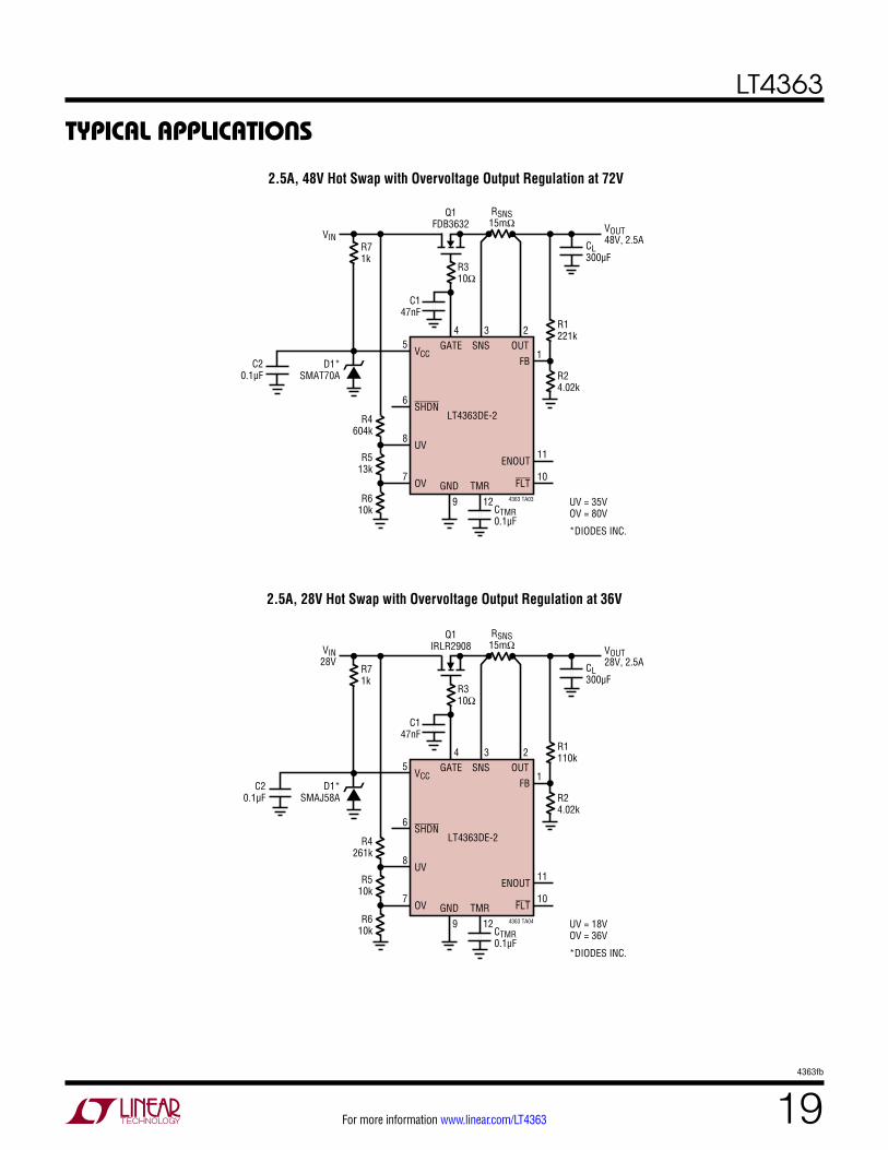
2.5A, 48V Hot Swap with Overvoltage Output Regulation at 72V
2.5A, 28V Hot Swap with Overvoltage Output Regulation at 36V
CTMR0.1µF
RSNS15mΩ
Q1FDB3632
VINVOUT48V, 2.5A
4363 TA03
LT4363DE-2
GND TMR9 12
OUT2
SNS3
FB1
D1*SMAT70A R2
4.02k
R1221k
R71k
GATE4
R310Ω
SHDN6
UV
*DIODES INC.
UV = 35VOV = 80V
8
VCC5
OV7
FLT
ENOUT10
11
CL300µF
R513k
R610k
R4604k
C147nF
C20.1µF
CTMR0.1µF
RSNS15mΩ
Q1IRLR2908VIN
28VVOUT28V, 2.5A
4363 TA04
LT4363DE-2
GND TMR9 12
OUT2
SNS3
FB1
D1*SMAJ58A R2
4.02k
R1110k
R71k
GATE4
R310Ω
SHDN6
UV
*DIODES INC.
UV = 18VOV = 36V
8
VCC5
OV7
FLT
ENOUT10
11
CL300µF
R510k
R610k
R4261k
C147nF
C20.1µF
LT4363
204363fb
For more information www.linear.com/LT4363
Typical applicaTions
Overvoltage Regulator with Reverse Input Protection Up to –80V
Overvoltage Regulator with 250V Surge Protection
CTMR0.1µF
RSNS10mΩ
Q1IRLR2908VIN
12VVOUT12V, 3ACLAMPEDAT 16V
4363 TA05
LT4363DE-2
GND TMR9 12
OUT2
SNS3
FB1
R24.99k
R157.6k
GATE4
VCC
5
R310Ω
*DIODES INC.**SANYO 25CE22GA***OPTIONAL COMPONENTFOR REDUCED STANDBY CURRENT
SHDN6
UV8
OV7
FLT
ENOUT10
11
CL**22µF
Q2IRLR2908
D1*SMAJ58CA
R710k
R51M
Q32N3904
D21N4148
D3**1N4148
R410Ω
C147nF
CTMR0.1µF
R310Ω
RSNS10mΩ
Q1FDB33N25
Q2MPS-A42
VIN12V
4363 TA07
LT4363DE-2
GND TMR
OUTGATE SNS
UV
SHDN
OV FAULT
OUTPUT CLAMP AT 16V
ENOUT
FLT
FB
D1*SMAJ58A
*DIODES INC.
CL22µF
C20.1µF VCC
DC/DCCONVERTER
GNDSHDN
VCCR24.99k
R4127k
R549.9k
R157.6kC1
47nF
R649.9k
9 12
23
1
45
6
8
7 10
11
LT4363
214363fb
For more information www.linear.com/LT4363
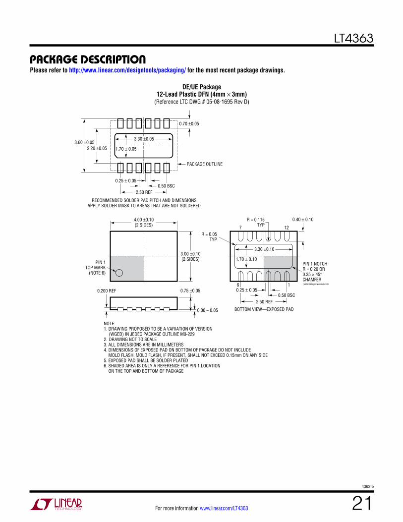
package DescripTionPlease refer to http://www.linear.com/designtools/packaging/ for the most recent package drawings.
DE/UE Package12-Lead Plastic DFN (4mm × 3mm)
(Reference LTC DWG # 05-08-1695 Rev D)
4.00 ±0.10(2 SIDES)
3.00 ±0.10(2 SIDES)
NOTE:1. DRAWING PROPOSED TO BE A VARIATION OF VERSION (WGED) IN JEDEC PACKAGE OUTLINE M0-2292. DRAWING NOT TO SCALE3. ALL DIMENSIONS ARE IN MILLIMETERS4. DIMENSIONS OF EXPOSED PAD ON BOTTOM OF PACKAGE DO NOT INCLUDE MOLD FLASH. MOLD FLASH, IF PRESENT, SHALL NOT EXCEED 0.15mm ON ANY SIDE5. EXPOSED PAD SHALL BE SOLDER PLATED6. SHADED AREA IS ONLY A REFERENCE FOR PIN 1 LOCATION ON THE TOP AND BOTTOM OF PACKAGE
0.40 ± 0.10
BOTTOM VIEW—EXPOSED PAD
1.70 ± 0.10
0.75 ±0.05
R = 0.115TYP
R = 0.05TYP
2.50 REF
16
127
PIN 1 NOTCHR = 0.20 OR0.35 × 45°CHAMFER
PIN 1TOP MARK
(NOTE 6)
0.200 REF
0.00 – 0.05
(UE12/DE12) DFN 0806 REV D
2.50 REF
RECOMMENDED SOLDER PAD PITCH AND DIMENSIONSAPPLY SOLDER MASK TO AREAS THAT ARE NOT SOLDERED
2.20 ±0.05
0.70 ±0.05
3.60 ±0.05
PACKAGE OUTLINE
3.30 ±0.10
0.25 ± 0.050.50 BSC
1.70 ± 0.05
3.30 ±0.05
0.50 BSC0.25 ± 0.05
LT4363
224363fb
For more information www.linear.com/LT4363
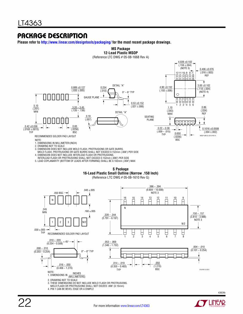
package DescripTionPlease refer to http://www.linear.com/designtools/packaging/ for the most recent package drawings.
MS Package12-Lead Plastic MSOP
(Reference LTC DWG # 05-08-1668 Rev A)
MSOP (MS12) 0213 REV A
0.53 ±0.152(.021 ±.006)
SEATINGPLANE
0.18(.007)
1.10(.043)MAX
0.22 – 0.38(.009 – .015)
TYP
0.86(.034)REF
0.650(.0256)
BSC
12 11 10 9 8 7
NOTE:1. DIMENSIONS IN MILLIMETER/(INCH)2. DRAWING NOT TO SCALE3. DIMENSION DOES NOT INCLUDE MOLD FLASH, PROTRUSIONS OR GATE BURRS. MOLD FLASH, PROTRUSIONS OR GATE BURRS SHALL NOT EXCEED 0.152mm (.006") PER SIDE4. DIMENSION DOES NOT INCLUDE INTERLEAD FLASH OR PROTRUSIONS. INTERLEAD FLASH OR PROTRUSIONS SHALL NOT EXCEED 0.152mm (.006") PER SIDE5. LEAD COPLANARITY (BOTTOM OF LEADS AFTER FORMING) SHALL BE 0.102mm (.004") MAX
0.254(.010) 0° – 6° TYP
DETAIL “A”
DETAIL “A”
GAUGE PLANE
5.10(.201)MIN
3.20 – 3.45(.126 – .136)
0.889 ±0.127(.035 ±.005)
RECOMMENDED SOLDER PAD LAYOUT
0.42 ±0.038(.0165 ±.0015)
TYP
0.65(.0256)
BSC
4.039 ±0.102(.159 ±.004)
(NOTE 3)
0.1016 ±0.0508(.004 ±.002)
1 2 3 4 5 6
3.00 ±0.102(.118 ±.004)
(NOTE 4)
0.406 ±0.076(.016 ±.003)
REF
4.90 ±0.152(.193 ±.006)
.016 – .050(0.406 – 1.270)
.010 – .020(0.254 – 0.508)
× 45°
0° – 8° TYP.008 – .010
(0.203 – 0.254)
1
N
2 3 4 5 6 7 8
N/2
.150 – .157(3.810 – 3.988)
NOTE 3
16 15 14 13
.386 – .394(9.804 – 10.008)
NOTE 3
.228 – .244(5.791 – 6.197)
12 11 10 9
S16 REV G 0212
.053 – .069(1.346 – 1.752)
.014 – .019(0.355 – 0.483)
TYP
.004 – .010(0.101 – 0.254)
.050(1.270)
BSC
.245MIN
N
1 2 3 N/2
.160 ±.005
RECOMMENDED SOLDER PAD LAYOUT
.045 ±.005 .050 BSC
.030 ±.005 TYP
INCHES(MILLIMETERS)
NOTE:1. DIMENSIONS IN
2. DRAWING NOT TO SCALE3. THESE DIMENSIONS DO NOT INCLUDE MOLD FLASH OR PROTRUSIONS. MOLD FLASH OR PROTRUSIONS SHALL NOT EXCEED .006" (0.15mm)4. PIN 1 CAN BE BEVEL EDGE OR A DIMPLE
S Package16-Lead Plastic Small Outline (Narrow .150 Inch)
(Reference LTC DWG # 05-08-1610 Rev G)
LT4363
234363fb
For more information www.linear.com/LT4363
Information furnished by Linear Technology Corporation is believed to be accurate and reliable. However, no responsibility is assumed for its use. Linear Technology Corporation makes no representa-tion that the interconnection of its circuits as described herein will not infringe on existing patent rights.
revision hisToryREV DATE DESCRIPTION PAGE NUMBER
A 3/12 Add 57.6k resistor to Typical Application 24
B 6/13 Added H and MP temperature grades to Order InformationOperating Voltage Range for all temperature grades is 4V to 80VReverse Input Current maximum changed to –4mA from –3mAIGATE(UP): At 12V, changed from [–10, –20, –35]µA to [–15, –30, –45]µA. At 48V, changed from [–10, –25, –40]µA to [–20, –40, –65]µACurrent Limit Sense Voltage: At 12V, improved from 43mV — 58mV to 45mV — 55mV. At 48V, improved from 45mV — 59mV to 48mV — 58mVISNS maximum changed from 30µA to 40µAVTMR(H) range changed from 3.7V — 5V to 3.5V — 5.4VOUT Reset Threshold minimum changed from 1.9V to 1.8VUpdated curves in graphs G05, G06 and G09Corrected Y-axis numbers in Warning Period TMR Current, graph G15Replaced Current Limit at Supply Voltage graph with Current Limit FoldbackGATE Pin Description: Added information on 14V protection clampTMR Pin Description: Added 10nF minimum capacitor requirementChanged GATE to SNS clamp in Block Diagram to 14V from 13VAdded 0.1µF C2 to Typical Application circuits
333 3 4444567889
18, 19
LT4363
244363fb
For more information www.linear.com/LT4363
Linear Technology Corporation1630 McCarthy Blvd., Milpitas, CA 95035-7417
LINEAR TECHNOLOGY CORPORATION 2011
LT 0613 REV B • PRINTED IN USA
(408) 432-1900 FAX: (408) 434-0507 www.linear.com/LT4363
relaTeD parTs
Typical applicaTionOvervoltage Regulator with Ideal Diode Reverse Voltage Protection
PART NUMBER DESCRIPTION COMMENTS
LTC1696 Overvoltage Protection Controller ThinSOT™ Package, 2.7V to 27V
LTC2909 Triple/Dual Inputs UV/OV Negative Monitor Pin Selectable Input Polarity Allows Negative and OV Monitoring
LTC2912/LTC2913 Single/Dual UV/OV Voltage Monitor Ads UV and OV Trip Values, ±1.5% Threshold Accuracy
LTC2914 Quad UV/OV Monitor For Positive and Negative Supplies
LTC3827/LTC3827-1 Low IQ, Dual, Synchronous Controller 4V ≤ VIN ≤ 36V, 0.8V ≤ VOUT ≤ 10V, 80µA Quiescent Current
LTC3835/LTC3835-1 Low IQ, Synchronous Step-Down Controller Single Channel LTC3827/LTC3827-1
LT3845 Low IQ, Synchronous Step-Down Controller 4V ≤ VIN ≤ 60V, 1.23V ≤ VOUT ≤ 36V, 120µA Quiescent Current
LT3850 Dual, 550kHz, 2-Phase Synchronous Step-Down Controller
Dual 180° Phased Controllers, VIN 4V to 24V, 97% Duty Cycle, 4mm × 4mm QFN-28, SSOP-28 Packages
LTC3890 Low IQ, Dual 2-Phase, Synchronous Step-Down Controller
4V ≤ VIN ≤ 60V, 0.8V ≤ VOUT ≤ 24V, 50µA Quiescent Current
LT4256-1 Positive 48V Hot Swap Controller with Open-Circuit Detect
Foldback Current Limiting, Open-Circuit and Overcurrent Fault Output, Up to 80V Supply
LTC4260 Positive High Voltage Hot Swap Controller with 8-Bit ADC and I2C
Wide Operating Range 8.5V to 80V
LTC4352 Ideal MOSFET ORing Diode External N-Channel MOSFETs Replace ORing Diodes, 0V to 18V
LTC4354 Negative Voltage Diode-OR Controller Controls Two N-Channel MOSFETs, 1µs Turn-Off, 80V Operation
LTC4355 Positive Voltage Diode-OR Controller Controls Two N-Channel MOSFETs, 0.3µs Turn-Off, 80V Operation
LT4356-1 High Voltage Surge Stopper 100V Overvoltage and Overcurrent Protection, Latch-Off and Auto-Retry Options
LTC4364 Surge Stopper with Ideal Diode 4V to 80V Operation; –40V Reverse Input, –20V Reverse Output Protection
LTC4365 Window Passer - OV, UV and Reverse Supply Protection Controller
2.5V to 34V Operation, Protects 60V to –40V
0.1µF
10mΩIRLR2908 OUTPUTCLAMPAT 16V
4363 TA06
LT4363
GND TMR
OUTSNS
FB
47nF
4.99k
57.6kGATEVCC
10Ω
–60V TO 75V DC PROTECTION100V TRANSIENT MAXIMUMUV = 4.5V
SHDN
UV
DC/DCCONVERTER
GND
SHDN
VCC
FLT FAULT
ENOUT
22µF
49.9k
127k
LTC4357
GND
IN OUT
VDD
GATE
M1FDB3632VIN
12V
D1MMBD1205
DCLAMPSMAT70A