L28 April 281 EE5342 – Semiconductor Device Modeling and Characterization Lecture 28 - Spring 2005...
26
L28 April 28 1 EE5342 – Semiconductor Device Modeling and Characterization Lecture 28 - Spring 2005 Professor Ronald L. Carter [email protected] http://www.uta.edu/ronc/
-
Upload
louise-alison-holmes -
Category
Documents
-
view
222 -
download
0
Transcript of L28 April 281 EE5342 – Semiconductor Device Modeling and Characterization Lecture 28 - Spring 2005...

L28 April 28 1
EE5342 – Semiconductor Device Modeling and CharacterizationLecture 28 - Spring 2005
Professor Ronald L. [email protected]
http://www.uta.edu/ronc/

L28 April 28 2
MOSFET circuitparameters
region ohmic ,VL
'CWg
saturation ,VVL
'CWg
V
Ig
cetancTranscondu
DSOxn
mL
TGSOxn
ms
VGS
Dm
DS

L28 April 28 3
Estimating LAMBDA
0V,
qN
VV22x
,V
x
x1
VL
L1
is of tioninterpreta The
V1VVLW
2'C
I
SBa
SBDSp
maxd,
DS
max,d
max,dDS
DS2
TGSOxn
sat,D

L28 April 28 4
SPICE mosfet Model Instance CARM*, Ch. 4, p. 290M MOSFET
General Form
M<name> <drain node> <gate node> <source node>+ <bulk/substrate node> <model name>+ [L=<value>] [W=<value>]+ [AD=<value>] [AS=<value>]+ [PD=<value>] [PS=<value>]+ [NRD=<value>] [NRS=<value>]+ [NRG=<value>] [NRB=<value>]+ [M=<value>]
Examples
M1 14 2 13 0 PNOM L=25u W=12uM13 15 3 0 0 PSTRONGM16 17 3 0 0 PSTRONG M=2M28 0 2 100 100 NWEAK L=33u W=12u+ AD=288p AS=288p PD=60u PS=60u NRD=14 NRS=24 NRG=10
L = Ch. L. [m]W = Ch. W. [m]AD = Drain A [m2]AS = Source A[m2]NRD, NRS = D and S diff in squares
M = device multiplier
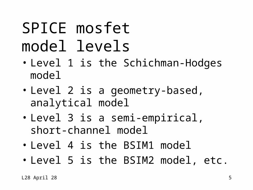
L28 April 28 5
SPICE mosfet model levels• Level 1 is the Schichman-Hodges
model• Level 2 is a geometry-based,
analytical model• Level 3 is a semi-empirical, short-
channel model• Level 4 is the BSIM1 model• Level 5 is the BSIM2 model, etc.

L28 April 28 6
SPICE ParametersLevel 1 - 3 (Static)Par am. Parameter Description Def . Typ. Units
VTO Zero-bias Vthresh 1 1 V
KP Transconductance 2.E-05 3.E-05 A/ V 2̂
GAMMA Body-eff ect par. 0.0 0.35 V 1̂/ 2
PHI Surf ace inversion pot. 0.6 0.65 V
LAMBDA Channel-length mod. 0.0 0.02 1/ V
TOX Thin oxide thickness 1.E-07 1.E-07 m
NSUB Substrate doping 0.0 1.E+15 cm̂ -3
NSS Surf ace state density 0.0 1.E+10 cm̂ -2
LD Lateral diff usion 0.0 8.E-05 m
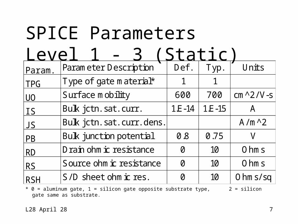
L28 April 28 7
Par am. Parameter Description Def . Typ. Units
TPG Type of gate material* 1 1
UO Surf ace mobility 600 700 cm̂ 2/ V-s
I S Bulk j ctn. sat. curr. 1.E-14 1.E-15 A
J S Bulk j ctn. sat. curr. dens. A/ m̂ 2
PB Bulk junction potential 0.8 0.75 V
RD Drain ohmic resistance 0 10 Ohms
RS Source ohmic resistance 0 10 Ohms
RSH S/ D sheet ohmic res. 0 10 Ohms/ sq
SPICE ParametersLevel 1 - 3 (Static)
* 0 = aluminum gate, 1 = silicon gate opposite substrate type, 2 = silicon gate same as substrate.
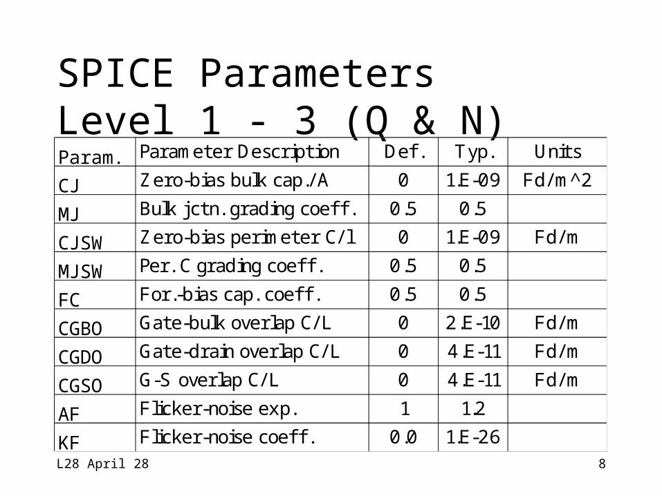
L28 April 28 8
SPICE ParametersLevel 1 - 3 (Q & N)Par am. Parameter Description Def . Typ. Units
CJ Zero-bias bulk cap./ A 0 1.E-09 Fd/ m̂ 2
MJ Bulk j ctn. grading coeff . 0.5 0.5
CJ SW Zero-bias perimeter C/ l 0 1.E-09 Fd/ m
MJ SW Per. C grading coeff . 0.5 0.5
FC For.-bias cap. coeff . 0.5 0.5
CGBO Gate-bulk overlap C/ L 0 2.E-10 Fd/ m
CGDO Gate-drain overlap C/ L 0 4.E-11 Fd/ m
CGSO G-S overlap C/ L 0 4.E-11 Fd/ m
AF Flicker-noise exp. 1 1.2
KF Flicker-noise coeff . 0.0 1.E-26

L28 April 28 9
Level 1 Static Const.For Device EquationsVfb = -TPG*EG/2 -Vt*ln(NSUB/ni)
- q*NSS*TOX/eOxVTO = as given, or
= Vfb + PHI + GAMMA*sqrt(PHI)KP = as given, or = UO*eOx/TOXCAPS are spice pars., technological
constants are lower case

L28 April 28 10
Level 1 Static Const.For Device Equations = KP*[W/(L-2*LD)] = 2*K, K not spiceGAMMA = as given, or = TOX*sqrt(2*eSi*q*NSUB)/eOx2*phiP = PHI = as given, or = 2*Vt*ln(NSUB/ni)ISD = as given, or = JS*AD
ISS = as given, or = JS*AS
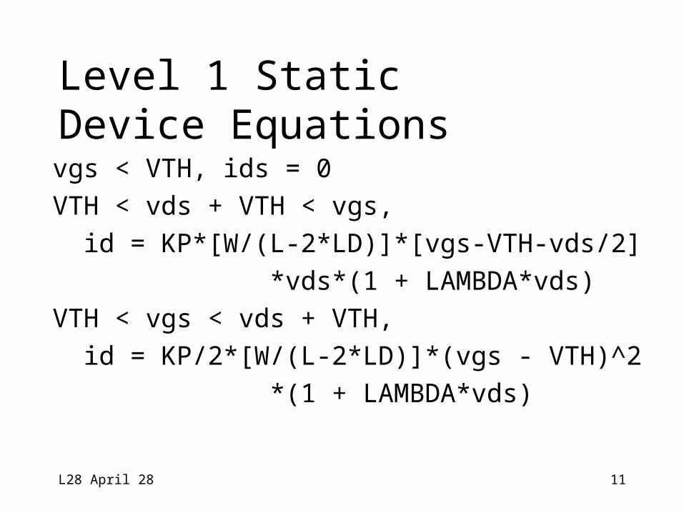
L28 April 28 11
Level 1 Static Device Equationsvgs < VTH, ids = 0VTH < vds + VTH < vgs, id = KP*[W/(L-2*LD)]*[vgs-VTH-vds/2] *vds*(1 + LAMBDA*vds)VTH < vgs < vds + VTH, id = KP/2*[W/(L-2*LD)]*(vgs - VTH)^2 *(1 + LAMBDA*vds)

L28 April 28 12
e-e- e- e- e- + + + + + + + + + +
+ +
n-channel enhancementMOSFET in ohmic region
0< VT< VG
VB < 0
EOx,x> 0
Acceptors
Depl Reg
VS = 0 0< VD<
VDS,sat n+
n+
p-substrate
Channel
e- channel ele + implant ion

L28 April 28 13
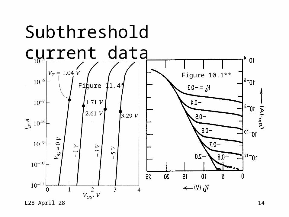
Subthreshold conduction• Below O.S.I., when the total band-
bending < 2|p|, the weakly inverted channel conducts by diffusion like a BJT.
• Since VGS>VDS, and below OSI, then Na>nS >nD, and electr diffuse S --> D
t
DS
t
GSsubthresh,D V
Vexp1
VV
expI
Electron concentration at Source
Concentration gradient driving diffusion
L28 April 28 14
Subthreshold current data
Figure 11.4*
Figure 10.1**
L28 April 28 15
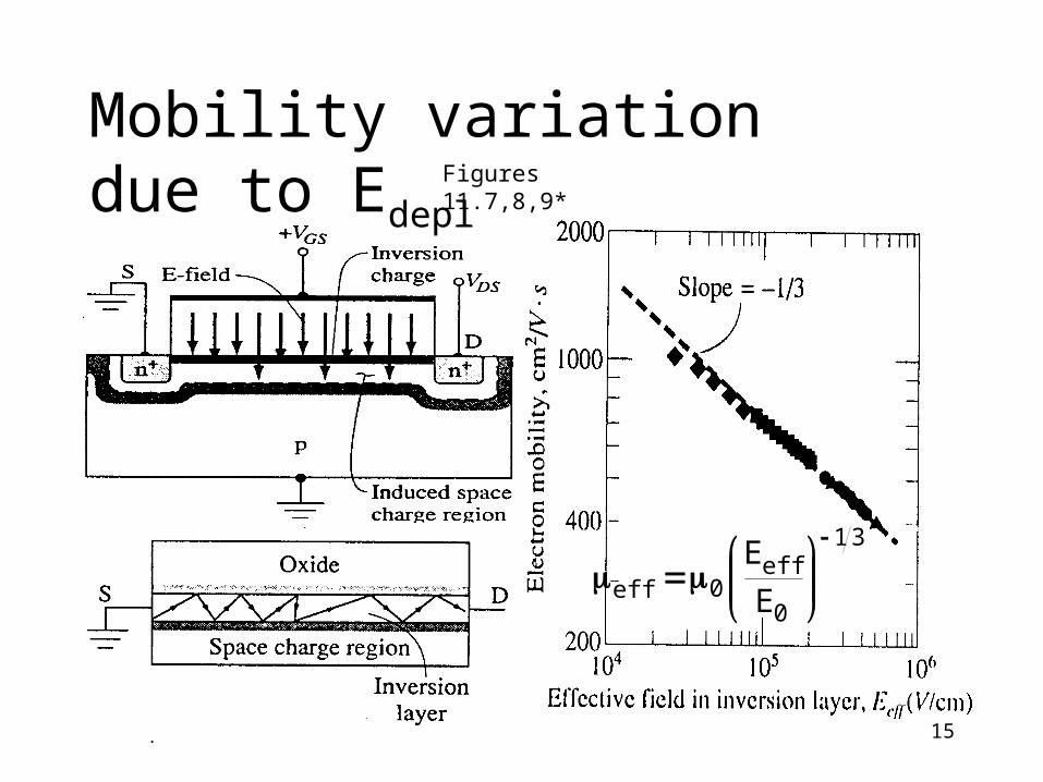
Mobility variationdue to Edepl
Figures 11.7,8,9*
31
0
eff0eff E
E

L28 April 28 16
Velocity saturationeffects
L2v
f
vWCg
E as vv So
v
E1
vv limit" speed"
satT
satOxsat,m
sat
212
sat
eff
eff
thsat
Figure 11.10*

L28 April 28 17
SPICE ParametersLevel 2Par am. Parameter Description Def . Typ. Units
NEFF Total channel chg coeff . 1 5
UCRI T Critical E-fi eld f or mob. 1.E+04 1.E+04 V/ cm
UEXP Expon. coeff . f or mob. 0 0.1
UTRA Transverse fi eld coeff . 0 0.5

L28 April 28 18
SPICE ParametersLevel 2 & 3Par am. Parameter Description Def . Typ. Units
NFS Surf ace-f ast state dens. 0.0 1.E+10 cm̂ -2
XJ Metallurgical j ctn. depth 0.0 1.E-06 m
VMAX Max. drif t v of carr. 0.0 5.E+04 m/ s
XQC Coeff . of ch. Q share 0.0 0.4
DELTA Width eff . on Vthresh 0.0 1.0

L28 April 28 19
Level 2 StaticDevice EquationsAccounts for variation of channel
potential for 0 < y < LFor vds < vds,sat = vgs - Vfb - PHI +
2*[1-sqrt(1+2(vgs-Vfb-vbs)/2]
id,ohmic = [/(1-LAMBDA*vds)] *[vgs - Vfb - PHI - vds/2]*vds -2[vds+PHI-vbs)1.5-(PHI-vbs)1.5]/3
L28 April 28 20
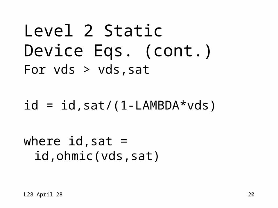
Level 2 StaticDevice Eqs. (cont.)For vds > vds,sat
id = id,sat/(1-LAMBDA*vds)
where id,sat = id,ohmic(vds,sat)

L28 April 28 21
Level 2 StaticDevice Eqs. (cont.)Mobility variationKP’ = KP*[(esi/eox)*UCRIT*TOX /(vgs-VTH-UTRA*vds)]UEXP
This replaces KP in all other formulae.

L28 April 28 22
SPICE ParametersLevel 3Par am. Parameter Description Def . Typ. Units
KAPPA Saturation fi eld f actor 0.2 1.0
ETA Stat. f eedbk on Vthresh 0.0 1.0
THETA Mobility modulation 0.0 0.05 1/ V
DELTA Width eff . on Vthresh 0.0 1.0

L28 April 28 23
Project 2 Parameter Values ExtractedIS " 891.8a" BF " 113.6 " NF " 1.044 " VAF " 83.50 " IKF " 13.45m" ISE " 20.40f" NE " 1.772 " BR " 2.270 " NR " 1.013 " VAR " 22.92 " IKR " 2.000m" ISC " 537.6f" NC " 1.675 "
RB " 1.233K" IRB " 1.000u" RBM " 151.8 " RE " 2.560 " RC " 26.00 " CJE " 2.344p" VJE " 762.0m" MJE " 344.9m" CJC " 1.234p" VJC " 570.8m" MJC " 347.6m" CJS " 100.4f" VJS " 566.0m" MJS " 267.0m"

L28 April 28 24
Project 2 Optimized Parameter ValuesIS " 890.9a"BF " 123.7 "NF " 1.043 "VAF " 86.04 "IKF " 14.33m"ISE " 28.54f"NE " 1.878 "BR " 2.657 "NR " 1.012 "VAR " 21.25 "IKR " 6.470m"ISC " 537.6f"NC " 1.675 "
RB " 1.233K"IRB " 986.9n"RBM " 122.2 "RE " 2.831 "RC " 11.71 "CJE " 2.344p"VJE " 762.0m"MJE " 344.9m"CJC " 1.234p"VJC " 570.8m"MJC " 347.6m"CJS " 100.4f"VJS " 566.0m"MJS " 267.0m"

L28 April 28 25
Project 2 Parameter Values Used for DataIS " 891.0a"BF " 123.0 "NF " 1.043 "VAF " 86.95 "IKF " 14.91m"ISE " 28.86f"NE " 1.876 "BR " 2.345 "NR " 1.012 "VAR " 23.45 "IKR " 23.45m"ISC " 1.095p"NC " 1.875 "
RB " 1.234K"IRB " 987.0n"RBM " 123.0 "RE " 2.345 "RC " 5.678 "CJE " 2.345p"VJE " 765.4m"MJE " 345.6m"CJC " 1.234p"VJC " 567.8m"MJC " 345.6m"CJS " 100.4f"VJS " 566.8m"MJS " 269.6m"
L28 April 28 26
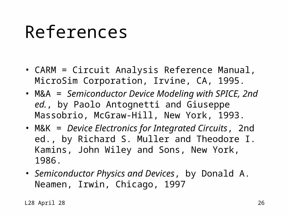
References
• CARM = Circuit Analysis Reference Manual, MicroSim Corporation, Irvine, CA, 1995.
• M&A = Semiconductor Device Modeling with SPICE, 2nd ed., by Paolo Antognetti and Giuseppe Massobrio, McGraw-Hill, New York, 1993.
• M&K = Device Electronics for Integrated Circuits, 2nd ed., by Richard S. Muller and Theodore I. Kamins, John Wiley and Sons, New York, 1986.
• Semiconductor Physics and Devices, by Donald A. Neamen, Irwin, Chicago, 1997