L14 March 31 EE5342 – Semiconductor Device Modeling and Characterization Lecture 14 - Spring 2005...
25
L14 March 3 1 EE5342 – Semiconductor Device Modeling and Characterization Lecture 14 - Spring 2005 Professor Ronald L. Carter [email protected] http://www.uta.edu/ronc/
-
Upload
charla-bradley -
Category
Documents
-
view
216 -
download
0
Transcript of L14 March 31 EE5342 – Semiconductor Device Modeling and Characterization Lecture 14 - Spring 2005...

L14 March 3 1
EE5342 – Semiconductor Device Modeling and CharacterizationLecture 14 - Spring 2005
Professor Ronald L. [email protected]
http://www.uta.edu/ronc/
L14 March 3 2
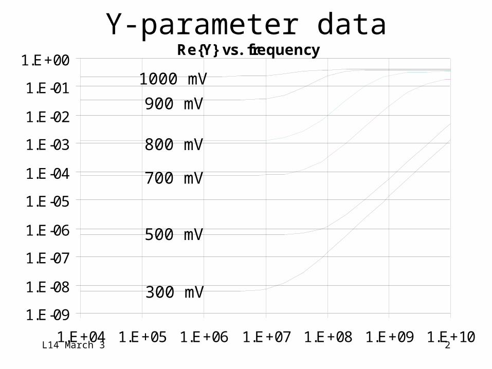
Re{Y} vs. frequency
1.E-09
1.E-08
1.E-07
1.E-06
1.E-05
1.E-04
1.E-03
1.E-02
1.E-01
1.E+00
1.E+04 1.E+05 1.E+06 1.E+07 1.E+08 1.E+09 1.E+10
Y-parameter data
300 mV
700 mV
1000 mV
800 mV
900 mV
500 mV
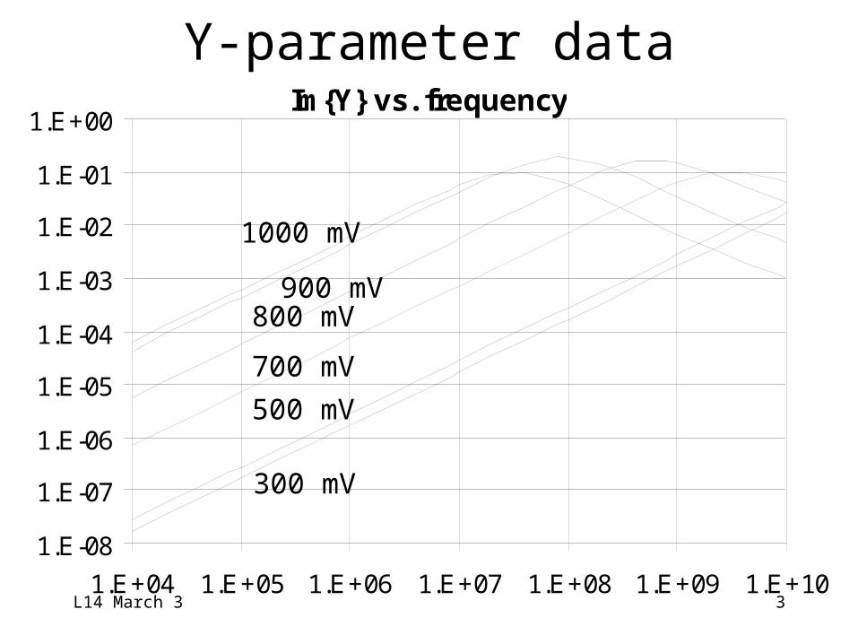
L14 March 3 3
Im{Y} vs. frequency
1.E-08
1.E-07
1.E-06
1.E-05
1.E-04
1.E-03
1.E-02
1.E-01
1.E+00
1.E+04 1.E+05 1.E+06 1.E+07 1.E+08 1.E+09 1.E+10
Y-parameter data
300 mV
700 mV
1000 mV
800 mV900 mV
500 mV

L14 March 3 4
Bipolar junctiontransistor (BJT)• The BJT is a “Si
sandwich” Pn (P=p+,=p-) or Np(N=n+, =n-)
• BJT action: npn Forward Active when VBE > 0 and VBC < 0
P n
E B C
VEB VCB
Charge neutral Region
Depletion Region

L14 March 3 5
BJT coordinatesystems
0
z
x”cx”
0 WB WB+WC-WE
0 xB x0x’Ex’
Charge neutral RegionDepletion Region
Base CollectorEmitter

L14 March 3 6
BJT boundary andinjection cond (npn)
0p
p , V
Vfexppp
0p
p , V
Vfexppp
C
C
2i
E
E
2i
x"xnC
Nn
0nCt
BC0nC0"xnC
x'xnE
Nn
0nEt
BE0nE0'xnE

L14 March 3 7
BJT boundary andinjection cond (npn)
.
V
Vfexpnn
n , V
Vfexpnn
dependent
-inter are BC Base the that Note
t
BC0pBxBxpB
Nn
0pBt
BE0pB0xpB
B
2i

L14 March 3 8
IC npn BJT(*Fig 9.2a)

L14 March 3 9
npn BJT bandsin FA region
qVBC
qVBE
q(VbiE-VBE ) q(VbiC-VBC )
injection high field
L14 March 3 10
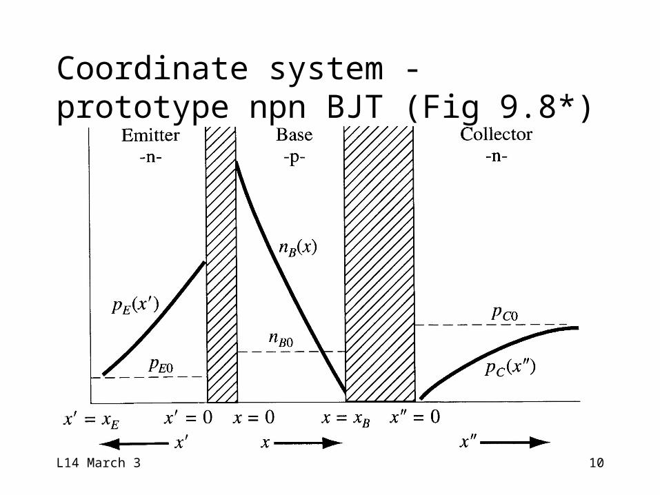
Coordinate system - prototype npn BJT (Fig 9.8*)

L14 March 3 11
Notation fornpn & pnp BJTs• NE, NB, NC E, B, and C doping (maj)
• xE, xB, xCE, B, and C CNR widths
• DE, DB, DC Dminority for E, B, and C
• LE, LB, LCLminority for E, B, and C(L2
min = Dmin min)
E0, B0, C0 minority carrier life- times for E, B, and C regions

L14 March 3 12
Notation fornpn BJTs only• pEO, nBO, pCO: E, B, and C thermal
equilibrium minority carrier conc
• pE(x’), nB(x), pC(x’’): positional mathe- matical function for the E, B, and C total minority carrier concentrations
pE(x’), nB(x), pC(x’’): positional ma- thematical function for the excess minority carriers in the E, B, and C

L14 March 3 13
Notation forpnp BJTs only• nEO, pBO, nCO: E, B, and C thermal
equilibrium minority carrier conc
• nE(x’), pB(x), nC (x’’): positional mathe- matical function for the E, B, and C total minority carrier concentrations
nE(x’), pB(x), nC(x’’): positional ma- thematical function for the excess minority carriers in the E, B, and C

L14 March 3 14
npn BJT boundary conditions
0xp ,1VV
expp0x"p :C
etc. ,Nn
n ,1VV
expnxn
,1V
Vexpn0xn :B
1V
Vexpp0p ,0xx'p :E
CCt
BC0CC
B
2i
0Bt
BC0BBB
t
BE0BB
t
BE0EEEE
L14 March 3 15
Emitter solutionin npn BJT
EEE
E
t
BE
E
E
E
E
t
BE
E
Lxx
xx
V
V
L
xL
xx
V
V
x
, '
1exppx'p
sinh
'sinh1expp
x'p
ppp , 0x'p
x'
'pD
E0E
E0
E
E0EE0
E2
E2
E

L14 March 3 16
Base solutionin npn BJT
Bt
BC
Bt
BEB0
BBBt
BC
B
B
t
BE
B
B
B0B
B0BB0BB
B2B
2
xx
VV
fxx
1V
Vfn
Lx when and Lx
VV
f
Lxx
V
Vf
Lx
nxn
nnn , 0D
xn
x
xn
expexp
sinhexp
sinhexpsinh

L14 March 3 17
Collector solutionin npn BJT
CCtBCC
C0C
C
C
C
C
t
BCC0
C
C0CC0CC
C2
C2
Lx , VV , L
"xpx"p
Lx
sinh
L"xx
sinh1VV
expp
x"p
ppp , 0D
x"p
x"
"xp

L14 March 3 18
Hyperbolic sinefunction
Lx
Lx
sinh0Lx
giving,
Lx
1Lx
1
Lx
1Lx
1
Lx
sinh L, x if so
...!2
yy1e ,
ee
eeLx
sinh
itlim
2y
L/xL/x
L/xL/x

L14 March 3 19
npn BJT regionsof operation
VBE
VBC
Forward Active
Reverse Active
Saturation
Cutoff

L14 March 3 20
npn FA BJT minoritycarrier distribution (Fig 9.4*)

L14 March 3 21
npn RA BJT minoritycarrier distribution (Fig 9.11a*)

L14 March 3 22
npn cutoff BJT mincarrier distribution (Fig 9.10a*)

L14 March 3 23
npn sat BJT minoritycarrier distribution (Fig 9.10b*)

L14 March 3 24
Defining currents inFA mode npn BJT (Fig 9.13*)

L14 March 3 25
References
1 OrCAD PSpice A/D Manual, Version 9.1, November, 1999, OrCAD, Inc.
2 Semiconductor Device Modeling with SPICE, 2nd ed., by Massobrio and Antognetti, McGraw Hill, NY, 1993.
* Semiconductor Physics & Devices, by Donald A. Neamen, Irwin, Chicago, 1997.