
Fabrication and Characterization of 0.2 m...
5
JOURNAL OF SEMICONDUCTOR TECHNOLOGY AND SCIENCE, VOL.1, NO. 2, JUNE, 2001 111 Fabrication and Characterization of 0.2µm InAlAs/InGaAs Metamorphic HEMT’s with Inverse Step-Graded InAlAs Buffer on GaAs Substrate Dae-Hyun Kim, Sung-Won Kim, Seong-Chul Hong, Seung-Won Paek, Jae-Hak Lee, Ki- Woong Chung, and Kwang-Seok Seo Abstract − Metamorphic InAlAs/InGaAs HEMT are successfully demonstrated, exhibiting several advantages over conventional P-HEMT on GaAs and LM-HEMT on InP substrate. The strain-relaxed metamorphic structure is grown by MBE on the GaAs substrate with the inverse-step graded InAlAs metamorphic buffer. The device with 40% indium content shows the better characteristics than the device with 53% indium content. The fabricated metamorphic HEMT with 0.2µm T-gate and 40% indium content shows the excellent DC and microwave characteristics of V th =-0.65V, g m,max =620 mS/mm, f T =120GHz and f max =210GHz. Index Terms− GaAs, HEMT, InGaAs, metamorphic, M-HEMT, Power I. INTRODUCTION While InAlAs/InGaAs HEMT’s (High Electron Mobility Transistors) on InP substrates exhibit the high gain and low noise characteristics at millimeter-wave frequencies, their small on-state breakdown voltages have limited their use in power applications [1-2]. Conversely, GaAs P-HEMT’s show the excellent power and gain performance at microwave frequencies, but their millimeter-wave performances are limited by the relatively small f T (unity gain cut-off frequency) and f max (maximum oscillation of frequency). These limitations can be solved by using metamorphic HEMT technologies: the growth of high In content on GaAs substrate. For the recent years, there has been considerable interest on the development of metamorphic-based HEMT (M-HEMT) devices [3-5]. The metamorphic structures using graded In(Ga)AlAs buffer or AlGaAsSb buffer can give a free choice of lattice constant and indium composition. M-HEMT’s provide the ability to tailor the lattice constant to any indium content desired, and therefore allow the device designer an additional degree of freedom to optimize the device performance with respect to high frequency gain, power, and noise. In this paper, we show the excellent performance of InGaAs/InAlAs M-HEMT’s with 40% and 53% Indium content. The device with lower indium content (40%) offers several advantages over InP-based HEMT. The relatively high band-gap of the InGaAs channel (~1eV) reduces the impact ionization effects in the channel, and the high bandgap of the InAlAs Schottky barrier layer increases the gate turn-on voltage. These two features can improve the device power performance with the increase of the drain breakdown voltage and the operational gate voltage swing. II. MATERIALS AND PROCESSING Manuscript received June 10, 2001; revised June 25, 2001. The authors are with School of Electrical Engineering & Computer Science, Seoul National University San 56-1, Shinlim-dong, Kwanak- gu, Seoul, 151-742, Korea (e-mail : [email protected]) Tel : +82-2-880-5451 Metamorphic InGaAs/InAlAs HEMT layers were grown by solid-source molecular beam epitaxy on 3 inch semi-insulating GaAs substrates. The metamorphic
Transcript of Fabrication and Characterization of 0.2 m...
JOURNAL OF SEMICONDUCTOR TECHNOLOGY AND SCIENCE, VOL.1, NO. 2, JUNE, 2001
111
Fabrication and Characterization of 0.2µm InAlAs/InGaAs Metamorphic HEMT’s with Inverse
Step-Graded InAlAs Buffer on GaAs Substrate
Dae-Hyun Kim, Sung-Won Kim, Seong-Chul Hong, Seung-Won Paek, Jae-Hak Lee, Ki-Woong Chung, and Kwang-Seok Seo
Abstract− Metamorphic InAlAs/InGaAs HEMT are successfully demonstrated, exhibiting several advantages over conventional P-HEMT on GaAs and LM-HEMT on InP substrate. The strain-relaxed metamorphic structure is grown by MBE on the GaAs substrate with the inverse-step graded InAlAs metamorphic buffer. The device with 40% indium content shows the better characteristics than the device with 53% indium content. The fabricated metamorphic HEMT with 0.2µm T-gate and 40% indium content shows the excellent DC and microwave characteristics of Vth=-0.65V, gm,max=620 mS/mm, fT=120GHz and fmax=210GHz.
Index Terms− GaAs, HEMT, InGaAs, metamorphic, M-HEMT, Power
I. INTRODUCTION
While InAlAs/InGaAs HEMT’s (High Electron Mobility Transistors) on InP substrates exhibit the high gain and low noise characteristics at millimeter-wave frequencies, their small on-state breakdown voltages have limited their use in power applications [1-2]. Conversely, GaAs P-HEMT’s show the excellent power and gain performance at microwave frequencies, but
their millimeter-wave performances are limited by the relatively small fT (unity gain cut-off frequency) and fmax (maximum oscillation of frequency). These limitations can be solved by using metamorphic HEMT technologies: the growth of high In content on GaAs substrate.
For the recent years, there has been considerable interest on the development of metamorphic-based HEMT (M-HEMT) devices [3-5]. The metamorphic structures using graded In(Ga)AlAs buffer or AlGaAsSb buffer can give a free choice of lattice constant and indium composition. M-HEMT’s provide the ability to tailor the lattice constant to any indium content desired, and therefore allow the device designer an additional degree of freedom to optimize the device performance with respect to high frequency gain, power, and noise.
In this paper, we show the excellent performance of InGaAs/InAlAs M-HEMT’s with 40% and 53% Indium content. The device with lower indium content (40%) offers several advantages over InP-based HEMT. The relatively high band-gap of the InGaAs channel (~1eV) reduces the impact ionization effects in the channel, and the high bandgap of the InAlAs Schottky barrier layer increases the gate turn-on voltage. These two features can improve the device power performance with the increase of the drain breakdown voltage and the operational gate voltage swing.
II. MATERIALS AND PROCESSING Manuscript received June 10, 2001; revised June 25, 2001. The authors are with School of Electrical Engineering & Computer
Science, Seoul National University San 56-1, Shinlim-dong, Kwanak-gu, Seoul, 151-742, Korea (e-mail : [email protected]) Tel : +82-2-880-5451
Metamorphic InGaAs/InAlAs HEMT layers were grown by solid-source molecular beam epitaxy on 3 inch semi-insulating GaAs substrates. The metamorphic

D. H. KIM et al. : FABRICATION AND CHARACTERIZATION OF 0.2µm InAls/InGaAs METAMORPHIC HEMT'S…
112
buffer consists of a 1-µm thick inverse step-graded InAlAs layer. The InAlAs /InGaAs MHEMT epitaxial structures are shown in Fig. 1. The results of Hall measurements indicate the 2-DEG density of 3.93 x 1012 cm-2 with the mobility of 7,780 cm2/V-s at 300K for sample-A (40% indium) and the 2-DEG density of 4.53 x 1012 cm-2 with the mobility of 8,000 cm2/V-s at 300K for sample-B (53% indium). These results are superior to those reported for GaAs P-HEMT’s, confirming the superiority of the electron transport characteristics of M-HEMT’s over GaAs P-HEMT’s.
(a)
S.I. GaAs Substrate
I InAlAs Buffer 1000A
δ -doping
Spacer
InxAlAs Graded M-Buffer
X=0.6
X=0
i InAlAs Barrier
n+ InGaAs Cap. 2.5X10
i InGaAs Channel 300A
(b)
Fig. 1. Cross-section of the InGaAs/InAlAs M-HEMT structures on GaAs substrate. (a) 40% Indium Content : Sample-A (b) 53% Indium Content : Sample-B.
Device fabrication begins with mesa isolation down to
the InAlAs buffer layer by the wet chemical etching using H3PO4:H2O2:H2O mixture. For the ohmic contact formation, an image reversal photo-resist (AZ5214) was
used to achieve a well-defined profile for lift-off. To obtain the lowest contact resistance, various Ni/Ge/Au ohmic metal structures were evaporated and annealed at different temperatures and the transmission line measurements were made to extract the ohmic contact resistance. As shown in Fig. 2, the 300/800/1000Å Ni/Ge/Au metal structures, annealed at 320°C for 20 seconds in H2 ambient, drastically lowered the contact resistance to 0.1 Ω-mm for InAlAs/InGaAs metamorphic structure. The double e-beam exposure method was applied to define 0.2µm T-gate with PMMA/P(MMA-MAA)/PMMA tri-layer photo-resist in order to improve lift-off [6]. After the wet gate recess using diluted citric acid, the gate Schottky metals were e-gun evaporated with Ti/Pt/Au(5000 Å). In the final step, RPECVD Si3N4 and thick Ti/Au contact were deposited for device passivation and microwave probing pads [7].
Fig. 2. Contact resistance (Rc) versus the alloy temperatures for the various Ni/Ge/Au structure.
III. DC AND RF CHARACTERISTICS
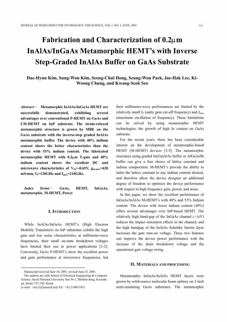
The 0.2µm T-Gate metamorphic HEMT’s were characterized on-wafer for dc and microwave performance. The output I-V transfer characteristics are shown in Fig. 3. The M-HEMT’s with 40% indium content exhibit Idss of 400mA/mm and gm,max of 630mS/mm with low output conductance (Go=5mS/mm @Vgs=0V & Vds=1.5V). The M-HEMT’s with 53% indium content show somewhat higher gm,max of 700mS/mm, but output conductance (Go=60mS/mm @Vgs=0V & Vds=1.5V) is about twelve times higher
JOURNAL OF SEMICONDUCTOR TECHNOLOGY AND SCIENCE, VOL.1, NO. 2, JUNE, 2001
113
than that of 40% indium content’s device. This means that as the indium content increases the carrier transport property is improved but the device gain characteristics are mainly limited by the impact ionization in the InGaAs channel. All devices show little kink effect that is often observed in the LM-HEMT’s on InP substrate [8].
0 2 4Vds [V]
0
200
400
600
Ids
[mA/
mm
]
Vgs=0V to -1.5V in -0.25V step
(a)
(b)
Fig. 3. Typical DC transfer I-V characteristics of the M-HEMT’s. A 40% In M-HEMT’s show that low output conductance and little kink effect. (a) 40% Indium content : Sample-A (b) 53% Indium content : Sample-B
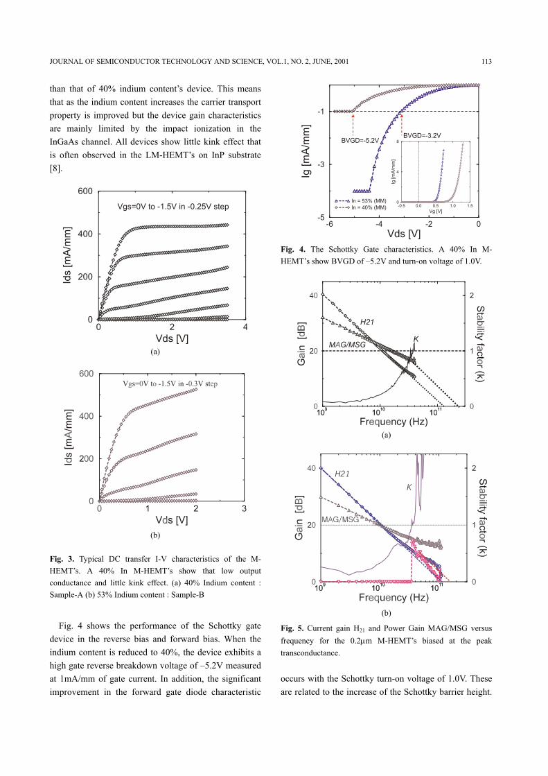
Fig. 4 shows the performance of the Schottky gate
device in the reverse bias and forward bias. When the indium content is reduced to 40%, the device exhibits a high gate reverse breakdown voltage of –5.2V measured at 1mA/mm of gate current. In addition, the significant improvement in the forward gate diode characteristic
-6 -4 -2 0Vds [V]
-5
-3
-1
Ig [m
A/m
m]
In = 53% (MM)In = 40% (MM)
BVGD=-5.2VBVGD=-3.2V
-0.5 0.0 0.5 1.0 1.5Vg [V]
0
4
8
Ig [m
A/m
m]
Fig. 4. The Schottky Gate characteristics. A 40% In M-HEMT’s show BVGD of –5.2V and turn-on voltage of 1.0V.
(a)
(b)
Fig. 5. Current gain H21 and Power Gain MAG/MSG versus frequency for the 0.2µm M-HEMT’s biased at the peak transconductance.
occurs with the Schottky turn-on voltage of 1.0V. These are related to the increase of the Schottky barrier height.

D. H. KIM et al. : FABRICATION AND CHARACTERIZATION OF 0.2µm InAls/InGaAs METAMORPHIC HEMT'S…
114
These two features enable to increase the operating gate voltage swing and therefore give rise to higher output power density, especially in the enhancement-mode power device.
The small-signal scattering parameters (S-parameters) of 2x100µm wide M-HEMT’s were measured using on-wafer probing and network analyzer (1 ~ 50GHz). With 40% indium content in the InGaAs channel layer, the better microwave performance is observed. Fig. 5. (a) shows the microwave characteristics for the sample-A (40% indium). A current gain cut-off frequency fT of 120GHz and an fmax of 210GHz are extrapolated from the H21 and the maximum available gain (MAG) for a 0.2µm device biased at the peak transconductance. Fig. 5. (b) shows the microwave gain characteristics for the sample-B (53% indium). A fT of 110GHz and an fmax of 160GHz are extrapolated from the H21 and the MAG. As similar to the dc characteristics, the microwave gain is also improved as the indium content decreases due to the reduced impact ionization in the channel layer.
IV. CONCLUSION
In summary, we have successfully demonstrated the InGaAs/InAlAs M-HEMT’s on GaAs substrate grown by MBE. The fabricated M-HEMT’s have the channel indium content of 40% and 53%, respectively. The M-HEMT with 40% indium content exhibits an fT of 120GHz and an fmax of 210GHz. This device also exhibits a high reverse breakdown voltage of –5.2V and forward gate turn-on voltage of 1.0V. These two results indicate that a higher output power density would result for the M-HEMT with 40% indium content due to the increased gate voltage swing. From the above results, the M-HEMT with 40% indium content would be a good compromise between the GaAs P-HEMT and LM-HEMT on InP substrate for power application at millimeter-wave frequency, because it enables to obtain excellent high-frequency performance, high current density, high breakdown voltage, and high gate turn-on voltage simultaneously.
ACKNOWLEDGMENTS
This work was supported financially by the National
Program for Tera-level Nano-devices of the Ministry of Science & Technology as one of the 21 Century Frontier Programs. The authors would like to thank Dr. Jiang Jian for epitaxial growth of metamorphic HEMT’s layer.
REFERENCES
[1] P. C. Chao, A. J. Tessmer, K. G. Duh, P. Ho, M. Kao, P. M. Smith, J. M. Ballingall, S. M. J. Liu and A. A. Jabra, “W-Band Low-Noise InAlAs/InGaAs Lattice-matched HEMT’s,” IEEE Electron Device Lett., vol. 11, pp. 59-62, Jan., 1990.
[2] P. M. Smith, “InP-based HEMTs for microwave and millimeter-wave applications,” in Proc. Indium Phosphide and related Conf., Sapporo, Japan, pp. 9-13, 1995.
[3] G. –W. Wang, Y. –K. Chen, W. J. Schaff, and L. F. Eastman, “A 0.1µm Al0.5In0.5As/Ga0.5In0.5As MODFET fabricated on GaAs substrate,” IEEE Trans. Electron Devices, vol. 35, pp. 818-823, 1988.
[4] Zaknoune, B. Bonter, C. Gaquiere, Y. cordier, Y.Druelle, D. Theron, and Y. Crosnier, “InAlAs/InGaAs metamorphic HEMT with high current density and high breakdown voltage,” IEEE Electron Device Lett., vol. 19, no. 9, pp. 345-347, 1998.
[5] D.M. Gill, B. Kane, S. Svensson, D. Tu, P. Uppal, and N. Byer, “High performance 0.1µm InAlAs/InGaAs high electron mobility transistors on GaAs,” IEEE Electron Device Lett., vol. 17, no. 7, pp. 228-230, 1996.
[6] N. Samoto, Y. Makino, K. Onda, E. Mizuki, and T. Itoh, “A novel electron-beam exposure technique for 0.1µm T-shpaed gate fabrication,” Journal of Vaccum Science and Technology, B8, pp. 1335-1338 , 1990.
[7] M.-K. Sohn, J. H. Lee, K. H. Kim, S. G. Yang, and K. S. Seo, “Remote PECVD Silicon Nitride Films with Improved Electrical Properties for GaAs P-HEMT Passivation,” Journal of the Korean Physical Society, vol. 33, pp. S379~S382, 1998.
[8] M. H. Somerville, J. A. Del Alamo, and W. Hoke, “ A new physical model for the kink effect on InAlAs/InGaAs HEMT’s,” in IEDM Tech. Dig., 1995, pp. 201-204
Dae-Hyun Kim was born in Korea on November 13, 1974. He received the B.S. degree in Electrical Engineering and Computer Science at Kyung-pook National University, Taegu, Korea, in 1997 and the M.S. degree in Electrical Engineering and Computer Science at Seoul National University, Seoul, Korea,

JOURNAL OF SEMICONDUCTOR TECHNOLOGY AND SCIENCE, VOL.1, NO. 2, JUNE, 2001
115
in 2000. Now he pursuits the Ph.D degree in Electrical Engineering and Computer Science at Seoul National University, Seoul, Korea. He worked at the Inter-university Semiconductor Research Center (ISRC), Seoul, Korea, from 1999 to 2001, where he engaged in the development of 0.5µm CMOS fabrication as a research assistant for the dry etching. His current interests include the development for the III-V HEMT’s device and the millimeter-wave MMIC’s.
Sung-Won Kim was born in Korea on May 6, 1975. He received the B.S. degree in Electrical Engineering and Computer Science at Kyung-pook National University, Taegu, Korea, in 2000. Now he pursuits the M.S. degree in Electrical Engineering and Computer Science at Seoul National University, Seoul, Korea. His current research
activities include the fabrication of 0.1µm,0.15µmGate-length HEMT's and their applications.
Seong-Chul Hong was born in Korea on October 13, 1975. He received the B.S. degree and the M.S. degree in Electrical Engineering and Computer Science at Seoul National University, Seoul, Korea, and in 1998 and 2001, respectively. Now he pursuits the Ph.D degree in Electrical Engineering and
Computer Science at Seoul National University, Seoul, Korea. His current research activities include the fabrication of 0.1µm,0.15µmGate-length HEMT's and their applications.
Seung-Won Paek was born in Incheon Korea on February 25, 1968. He received the B.S. degree, the M. S. degree, and the Ph. D. degree in Electronics Engineering at Seoul National University, Seoul, Korea in 1990, 1992, and 1999, respectively. In 1997, he joined LG Electronics Institute of Technology,
Seoul, Korea where he developed HEMT MMIC process and pin-diode MMIC process. In 2000, he joined Wavics Inc., Seoul, Korea. His current research interests include the design, fabrication and measurement of power HEMT devices.
Jae-Hak Lee received the B.S. degree in Electrical Engineering from Seoul National University, Seoul, Korea in 1988, the M. S. degree in Electronic and Electrical Engineering from Pohang University of Science and Technology, Pohang, Korea in 1990 and the Ph. D. degree in Electrical Engineering and
Computer Science from Seoul National University, Seoul, Korea in 2001, respectively. He worked at LG Electronics Institute of Technology, Seoul, Korea, from 1990 to 2001, where he engaged in the development of GaAs MESFET and HEMT MMIC processes. Currently, he is at Wavics Inc., Seoul, Korea. His present interests include III-V microwave and millimeter-wave device designs and process developments, and MMIC designs.
Ki-Woong Chung received the B.S. degree in Electrical Engineering from Seoul National University, Seoul, Korea in 1984, and the M. S. degree and the Ph. D. degree in Electrical and Electronic Engineering from Korea Advanced Institute of Science and Technology, Taejon, Korea in 1986, 1990, respectively. Between 1990 and 1991, he
has post doctoral course as a Research Associate in University of Minnesota, USA. In 1991, he joined at LG Electronics Institute of Technology, Seoul, Korea where he developed GaAs MESFET and HEMT MMIC processes and designs. In 2000, he is chief executive officer at Wavics Inc., Seoul, Korea. His current interests include III-V microwave and millimeter-wave circuit designs and process developments, RF MEMS devices and power semiconductor devices developments.
Kwang-Seok Seo received the B.S. degree from Seoul National University in 1976, and the M.S. degree from the Korea Advanced Institute of Science and Technology in 1978, and the Ph.D. degree on electrical engineering from the University of Michigan, Ann Arbor in 1987. From 1978 to 1982, he was a
senior research engineering at the korea Institute of electronics Technology. From 1987 to 1988, he was a postdoctoral fellow at the IBM T.J. Watson Research Center. Since 1989, he has been with Seoul National University, where he is now a Professor in the School of Electrical engineering and Computer science. His current interests include high speed device physics and technology, compound semiconductor.


![High-Throughput Low-Complexity Successive- Cancellation ...jsts.org/html/journal/journal_files/2015/06/Year... · The list SC decoder from A. Balatsoukas-Stimming et al. [14] shows](https://static.fdocuments.in/doc/165x107/5f8bd2f29292176e317a0c60/high-throughput-low-complexity-successive-cancellation-jstsorghtmljournaljournalfiles201506year.jpg)


