An Inductively Coupled Power and Data Link with Self...
9
JOURNAL OF SEMICONDUCTOR TECHNOLOGY AND SCIENCE, VOL.17, NO.1, FEBRUARY, 2017 ISSN(Print) 1598-1657 https://doi.org/10.5573/JSTS.2017.17.1.120 ISSN(Online) 2233-4866 Manuscript received Mar. 23, 2016; accepted Nov. 3, 2016 Department of Electronic Engineering, Inha University, Incheon 22212, South Korea E-mail : [email protected], [email protected] An Inductively Coupled Power and Data Link with Self-referenced ASK Demodulator and Wide-range LDO for Bio-implantable Devices Byeonggyu Park, Tae-Gwon Yun, Kyongsu Lee, and Jin-Ku Kang Abstract—This paper describes a neural stimulation system that employs an inductive coupling link to transfer power and data wirelessly. For the reliable data and power delivery, a self–referenced amplitude- shift keying (ASK) demodulator and a wide-range voltage regulator are suggested and implemented in the proposed stimulator system. The prototype fabricated in 0.35 um BCD process successfully transferred 1.2 Kbps data bi-directionally while supplying 4.5 mW power to internal MCU and stimulation block. Index Terms—Neural stimulator, near-field inductive coupling, maximum power transfer efficiency (PTE), implanted device I. INTRODUCTION Deep brain stimulators have been successfully demonstrated as a clinical tool for the treatment of chronic pain and movement disorders such as Parkinson’s disease [1-3]. These medical devices often employ the near-field inductive coupling for power and data delivery to implanted devices as a replacement for transcutaneous wires or implantable batteries that may cause infections in human body or require a periodic surgery. However, the small form factor requirement of these implants usually makes them difficult to deliver enough power for the internal circuits. Therefore, the efficiency of power transfer to the remotely powered implants has been one of the important issues and it is mainly limited by the weak inductive coupling [4, 5]. When the coupling distance and load condition are given, a careful choice of inductor topology should be made to utilize the maximum allowable power transfer efficiency (PTE). At the same time, the chip area and power consumption of the internal device should be kept to a minimum. Due to its simplicity, ASK scheme is often used for the data modulation in the implanted device. For the demodulation of the data from coupled ASK signal at the implanted device, it is necessary to build an extra regulator circuit for the reference voltage generation, consuming the chip area and power. Furthermore, the generated reference should not closely correlated to the signal to be detected so that the data recovery becomes insensitive to noise. To overcome the issue, a self- referenced ASK demodulation scheme is proposed for the reliable data demodulation with a low power consumption. During the power recovery, the operation range of internal circuits such as regulator and DC generator often limits the dynamic range. To solve this issue, we propose a wide-range voltage regulator to extend the operation range of the implanted device. This paper is organized as follows. In Section II, a system design methodology is described. In Section III, circuit designs including two proposed circuit blocks are discussed. The measurement results are presented in Section IV and conclusion is given in Section V.
Transcript of An Inductively Coupled Power and Data Link with Self...

JOURNAL OF SEMICONDUCTOR TECHNOLOGY AND SCIENCE, VOL.17, NO.1, FEBRUARY, 2017 ISSN(Print) 1598-1657 https://doi.org/10.5573/JSTS.2017.17.1.120 ISSN(Online) 2233-4866
Manuscript received Mar. 23, 2016; accepted Nov. 3, 2016 Department of Electronic Engineering, Inha University, Incheon 22212, South Korea E-mail : [email protected], [email protected]
An Inductively Coupled Power and Data Link with Self-referenced ASK Demodulator and Wide-range
LDO for Bio-implantable Devices
Byeonggyu Park, Tae-Gwon Yun, Kyongsu Lee, and Jin-Ku Kang
Abstract—This paper describes a neural stimulation system that employs an inductive coupling link to transfer power and data wirelessly. For the reliable data and power delivery, a self–referenced amplitude-shift keying (ASK) demodulator and a wide-range voltage regulator are suggested and implemented in the proposed stimulator system. The prototype fabricated in 0.35 um BCD process successfully transferred 1.2 Kbps data bi-directionally while supplying 4.5 mW power to internal MCU and stimulation block. Index Terms—Neural stimulator, near-field inductive coupling, maximum power transfer efficiency (PTE), implanted device
I. INTRODUCTION
Deep brain stimulators have been successfully demonstrated as a clinical tool for the treatment of chronic pain and movement disorders such as Parkinson’s disease [1-3]. These medical devices often employ the near-field inductive coupling for power and data delivery to implanted devices as a replacement for transcutaneous wires or implantable batteries that may cause infections in human body or require a periodic surgery. However, the small form factor requirement of these implants usually makes them difficult to deliver
enough power for the internal circuits. Therefore, the efficiency of power transfer to the
remotely powered implants has been one of the important issues and it is mainly limited by the weak inductive coupling [4, 5]. When the coupling distance and load condition are given, a careful choice of inductor topology should be made to utilize the maximum allowable power transfer efficiency (PTE). At the same time, the chip area and power consumption of the internal device should be kept to a minimum.
Due to its simplicity, ASK scheme is often used for the data modulation in the implanted device. For the demodulation of the data from coupled ASK signal at the implanted device, it is necessary to build an extra regulator circuit for the reference voltage generation, consuming the chip area and power. Furthermore, the generated reference should not closely correlated to the signal to be detected so that the data recovery becomes insensitive to noise. To overcome the issue, a self-referenced ASK demodulation scheme is proposed for the reliable data demodulation with a low power consumption.
During the power recovery, the operation range of internal circuits such as regulator and DC generator often limits the dynamic range. To solve this issue, we propose a wide-range voltage regulator to extend the operation range of the implanted device.
This paper is organized as follows. In Section II, a system design methodology is described. In Section III, circuit designs including two proposed circuit blocks are discussed. The measurement results are presented in Section IV and conclusion is given in Section V.

JOURNAL OF SEMICONDUCTOR TECHNOLOGY AND SCIENCE, VOL.17, NO.1, FEBRUARY, 2017 121
II. SYSTEM DESCRIPTION
The implanted stimulation system as shown in Fig. 1 consists of an external device for power and data delivery, inductive coupling interface, and internal device (or implanted device). A carrier frequency from external device delivers the power remotely to the internal device where a full rectifier and a voltage regulator recover DC power (3V) for the internal use. For the half-duplex data communication, transmitting data from an external device (downlink data) to an internal device is modulated with amplitude-shift-keying (ASK) and the data from internal device (uplink data) to an external device is modulated with load-shift-keying (LSK) [6]. The LSK modulation technique is to send the internal data (digital data) to the external device by changing the impedance of the resonance in the inductive link. If the impedance of the resonance circuit is changed by an internal switch, the output voltage level in the receiver side (external device) is varied and the change can be detected with LSK demodulator as an uplink data.
The two resonance circuits resonated at the carrier frequency amplifies the modulated signal and transfers data through the coupled inductor pair (L1, L2). The degree of inductive coupling is represented by the coupling coefficient (k), which is inversely proportional to the distance between two inductors. A typical distance (i.e. the thickness of tissue) for the neural stimulator ranges from 2 to 10 mm.
During transferring downlink data, the external device should deliver a continuous power to the internal circuits including a demodulator, a stimulator, a MCU (Micro-controller unit), and 4-channel electrodes. In transmitter a power amplifier (class-D type) drives low impedance series resonance circuits (L1 and C1). The downlink data transfers the configuration parameters for the stimulator and the MCU that chooses the combinations of channels to be activated and modulates the shape of stimulation signal. The uplink data transfers the status of the stimulation device to the external monitoring system.
When the inductors (a spiral trace on PCB) in the inductive link are to be designed, the PTE of inductive coupling system should be considered and it is heavily depends on the coupling factor (k) and the load in parallel with the secondary resonance circuits (L2 and C2). The coupling factor is inversely proportional to the
distance between inductors where its values ranges from 0.02 to 0.12. The transferred power through the inductively coupled links at the resonance is maximized at an optimal resistive load (RL,opt), which can be approximated as
2.
1 0 2
1 1 2L opt
QRk Q f Cp
= (1)
where 0f is the resonance frequency, 1Q is the quality
factors for the primary, and 2Q is the quality factor for the secondary resonator, respectively [6, 10].
In practice, the load (RL) is set by the power consumption of the internal circuit driven by the voltage regulator. Therefore, if the system parameters such as k, RL, f0, and Q values are known, the optimal inductance can be derived from the Eq. (1). This observation delivers a practical design procedure which is shown in Fig. 2. The validity of this design approach is based on the observation that the effective resistive load seen from the secondary coil (L2) is the sum of the series resistance of the full rectifier, the regulator and the load. When an optimal L2 is found then the next step is to design a
Fig. 1. The stimulation system block diagram.
Fig. 2. The design procedure for the stimulator system.
122 BYEONGGYU PARK et al : AN INDUCTIVELY COUPLED POWER AND DATA LINK WITH SELF-REFERENCED ASK …
resonance circuit with a given inductance and a Q factor with a field solver simulator in order to match with the measurement result of actual circuits on PCB. The k in this paper is chosen from the median value (0.06) of the range between 0.02 and 0.12. In this way, the optimal power transfer at given system parameters can be achieved. In this paper, we followed the design procedure in Fig. 2 to implement the proposed system.
Various design issues may occur while designing wireless ASK modulated data and power transceiver for the implanted device. The full-rectifier acts as an envelope detector and removes carrier frequency from the received signal in the implant. The full wave rectifier is realized by discrete devices with a diode bridge. The rectifier output (VREC) can be used as the ASK demodulator input to recover downlink data. However, the voltage level of VREC changes with respect to the coupling coefficient. Also, the voltage level of VREC changes with respect to the data pattern due to ASK modulated data transmission. Therefore the supply and reference voltage of the amplifier should track the common-mode level of VREC to recover data signal reliably. To achieve a reliable data recovery a self-referenced circuit technique for the ASK demodulator is proposed.
Secondly, a low-dropout (LDO) regulator with a band-gap reference (BGR) is used to provide a constant voltage to the internal circuits. However, the conventional regulators often exhibit a limited range with respect to its input voltage level (VREC). The lower boundary is due to the fact that the minimum voltage level is required to enable the BGR circuit. If the input of the reference generator is larger than a specific value, transistors in the BGR fall into the triode region failing to keep a constant reference level. This issue becomes more important in ASK modulated data transmission system since the output of regulator (VREG) is derived from the ASK modulated data. Therefore, a wide-range LDO topology covering the required VREC range reliably is proposed.
III. CIRCUIT IMPLEMENTATION
1. Inductor Design The first step of the proposed design procedure is to
determine design parameters such as RL, carrier frequency and the Q value of the resonance circuit. The design starts from the required power specification in the receiver. The power consumption of the internal circuits is targeted as 4.5 mW at 3 V supply. The higher carrier frequency, in general, suffers more attenuation in the body tissues [7] but supports the larger bandwidth for the data transfer. However, in typical stimulation system, the stimulus rate for stimulation is usually less than 1 Kbps [8]. The typical stimulation system does not require a high speed data rate. The Q factor of a spiral inductor on FR4 PCB is around 10 to 20. Based on these requirements, we set design parameters as RL=2 KΩ, carrier frequency = 6 MHz and Q = 15. From Eq. (1), we found the target inductance is about 3 uH at k=0.06 (the median value). The simulated PTE is the ratio of the recovered power at the secondary coil (PTE1) and the output of full rectifier (PTE2) in the implant to the transmitted power from the primary coil (Fig. 3). Fig. 3(a) presents that the PTE is maximized at about L=3 µH. At the target inductance, the PTE varies dramatically with respect to k as shown in Fig. 3(b). The maximum PTEs at k=0.12 are 71% and 48.3%, respectively. After the target inductance value is determined, the next step is to design a spiral inductor on PCB. The field solver simulations are performed to determine the geometric parameters (Fig. 4) such as the number of turns, outer dimension (X, Y), width, space and the size of hollow.
2. Proposed Self-referenced ASK Demodulator
The voltage range of VREC, which is the output of the
rectifier, is varying from 3 to 7 V. The ASK demodulator should decode directly the data as ‘0’or ‘1’ from the varying VREC value. The proposed self-referenced ASK demodulator consists of two amplifiers with passive
Fig. 3. Simulated PTE with respect to (a) the coil inductance, (b) the coupling coefficient.

JOURNAL OF SEMICONDUCTOR TECHNOLOGY AND SCIENCE, VOL.17, NO.1, FEBRUARY, 2017 123
components (Fig. 5(a)). A low-pass filter (R3 and C1) is used to extract the common-mode (CM) level of VREC and DC supply (Vs) to the amplifier. A resistive divider network (R1 and R2) is for lowering the amplifier input level (VIN). The CM of the VIN is filtered again by another filter (R4 and C2) and provides the reference (VREF_IN) for the amplifier. Thus the supply power and the reference voltage of the amplifier follow the CM level of VREC. With the proposed ASK demodulator, data is recovered reliably in the presence of VREC variations.
When a toggling pattern is applied to the demodulator (VREC) as shown in Fig. 5(b), VREF_IN stays in the middle of the VIN so that the amplifier can recover the data with a margin. In the simulation, the data can be successfully recovered with the two stage amplifiers with the detection margin of less than 20 mV.
The VIN is amplified if CM level of Vin+ and Vin- is between supply voltage and GND. The gain of this amplifier is small and the operating speed is slow because there is no bias current. Since the data rate in the wireless stimulator does not require a high speed, this amplifier is useful in wireless stimulator system with ASK demodulation where the CM level of VIN is not precisely defined. The proposed ASK demodulator consumes much less power (~200 µW), when compared to prior works in [12] and [13] that exhibit the power consumption of 1.01 mW and 0.481 mW, respectively.
3. Proposed Wide-range Voltage Regulator
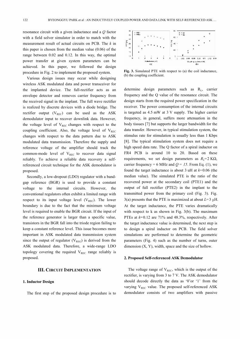
In conventional LDO regulators, the rectifier output is
directly connected to the supply voltage of a band-gap reference (BGR) as shown in Fig. 6. A cascoded BGR circuit in Fig. 7 is used for voltage regulator [9]. When all MOS transistors are operating in saturation region and the ratio of RA and RB is properly set, the cascaded BGR outputs VREF.
In conventional LDO with a cascoded BGR circuit, the minimum VREC which makes the BGR generate the constant VREF is the lower bound. When VREC becomes very large, then the BGR fails to generate a constant VREF since some transistors fall into the triode region. Thus, the operating range which the BGR generates the constant VREF limits the operating range of the LDO. In wireless stimulator, the operating region of the cascoded BGR should satisfy the condition, VREG<operation-range <VREG+VPEAK_REC while the level of VREC is varying by the modulated data pattern and k (coupling coefficient). VPEAK_REC is VHIGH - VLOW, where VHIGH and VLOW are the high and low amplitudes of the carrier corresponding data, respectively. In order to increase the output range of the BGR, all the MOS transistors should operate in saturation region under the higher VREC levels. For this, the current of BGR should be increased accordingly to keep the transistors saturation region, resultantly the power consumption increases.
Fig. 4. Design parameters of the spiral inductor for a field solver simulation.
Fig. 5. (a) Proposed self-referenced ASK demodulator circuit, (b) its simulation result.
124 BYEONGGYU PARK et al : AN INDUCTIVELY COUPLED POWER AND DATA LINK WITH SELF-REFERENCED ASK …
The cascoded BGR generates a reference voltage of 1.12 V when its power supply reaches a certain level (>3 V). The conventional LDO generates the desired level of VREG by feedback if BGR supplies the constant VREF. VREG is determined by the Eq. (2).
1 YREG REF
X
RV VR
æ ö= +ç ÷è ø
(2)
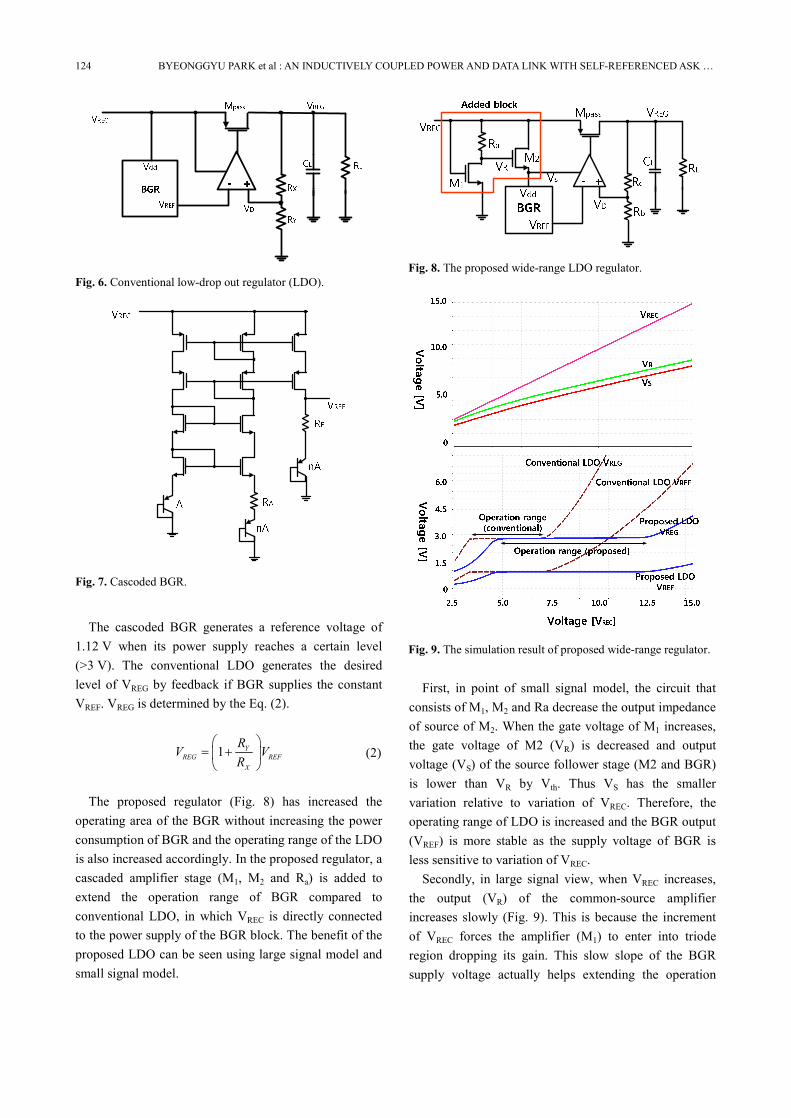
The proposed regulator (Fig. 8) has increased the
operating area of the BGR without increasing the power consumption of BGR and the operating range of the LDO is also increased accordingly. In the proposed regulator, a cascaded amplifier stage (M1, M2 and Ra) is added to extend the operation range of BGR compared to conventional LDO, in which VREC is directly connected to the power supply of the BGR block. The benefit of the proposed LDO can be seen using large signal model and small signal model.
First, in point of small signal model, the circuit that consists of M1, M2 and Ra decrease the output impedance of source of M2. When the gate voltage of M1 increases, the gate voltage of M2 (VR) is decreased and output voltage (VS) of the source follower stage (M2 and BGR) is lower than VR by Vth. Thus VS has the smaller variation relative to variation of VREC. Therefore, the operating range of LDO is increased and the BGR output (VREF) is more stable as the supply voltage of BGR is less sensitive to variation of VREC.
Secondly, in large signal view, when VREC increases, the output (VR) of the common-source amplifier increases slowly (Fig. 9). This is because the increment of VREC forces the amplifier (M1) to enter into triode region dropping its gain. This slow slope of the BGR supply voltage actually helps extending the operation
Fig. 6. Conventional low-drop out regulator (LDO).
Fig. 7. Cascoded BGR.
Fig. 8. The proposed wide-range LDO regulator.
Fig. 9. The simulation result of proposed wide-range regulator.

JOURNAL OF SEMICONDUCTOR TECHNOLOGY AND SCIENCE, VOL.17, NO.1, FEBRUARY, 2017 125
range. The output (Vs) of the M2 follows VR where its level is shifted by the threshold voltage. As shown in Fig. 9, the operation range of the proposed regulator is extended by 2.1 times. Proposed wide-range voltage regulator has power dissipation of 320 µW. The simulated line regulation is 14 mV/V, the load regulation is 0.05 mV/mA, and PSRR is 75 dB to 110 dB up to 10 MHz disturbance in the power line at Vin=8 V, Vout=3 V and load current=2 mA.
IV. MEASUREMENT RESULT
Based on the iterative simulations, actual spiral inductor patterns were fabricated on PCB. Several inductor patterns with slightly different geometric parameters (Fig. 4) are fabricated to match to the target inductance (3 uH) (Fig. 10(a)). A 2-oz metal thickness was used to secure high Q of the inductor. To measure the Q factor, a resonance circuit is designed to measure S11 and S21 with a network analyzer. The measured inductance was 3.4 uH and its Q factor (Fig. 10(b)) was 15.2 around 6 MHz.
The external and internal chips are fabricated in 0.35 um BCD process. The chip photographs are shown in Fig. 11. Each chip occupies 2.3x2.3 mm2. These chips are assembled on FR4 PCB by using COB process. A test setup for the power and data transfer is shown in Fig 11(c). A pattern generator with clock output is connected to the input of the ASK modulator and on-chip power amplifier to drive a series resonant circuit. The inductor pair was coupled to transfer power and data to the internal device. The regulator output at 2 KΩ load and the demodulator output were monitored with an oscilloscope. The on-chip power amplifier is connected to the series resonant circuit to measure the frequency
response (Fig. 12). The measured Q1 at 6 MHz was around 10.
The ASK modulated waveforms across the coupling inductors and demodulator output at the internal device are shown in Fig. 13(a). The proposed demodulator successfully recovered NRZ data delivered at 1.2 Kbps from the external device. The minimum resolution of the self-referenced demodulator was about 50 mV. Within 3 to 8 mm separation of coupling inductors, the regulator successfully supplies 4.5 mW power. The LSK modulated signal waveforms at the coupling inductors and recovered uplink data are shown in Fig. 13(b). The LSK demodulator in the external device successfully recovered uplink data at 1.2 Kbps. Measurement results for the operating area of the wide range LDO is shown in Fig. 14. It shows wider the operation area than operation
(a) (b)
Fig. 10. (a) Fabricated spiral inductor on PCB, (b) its S11 and S21 measurement result.
TX Coil RX
Fig. 11. Photographs of (a) external chip, (b) internal chip, (c) test setup.
Fig. 12. Measured frequency response of the primary resonant circuit.

126 BYEONGGYU PARK et al : AN INDUCTIVELY COUPLED POWER AND DATA LINK WITH SELF-REFERENCED ASK …
area of the conventional regulator. The performance of the stimulator system is summarized in Table 1. In Table 2, the performance of the proposed demodulator alone is compared with the prior works in the literatures [11-13]. The proposed self-referenced ASK demodulator consumes less area and power.
V. CONCLUSIONS
For the implementation of biomedical stimulator system, this paper described a practical design procedure that delivers the maximum allowable power at the given system requirements such as carrier frequency, inductor topology, and load condition. Self-referenced ASK demodulator and wide-range regulator topology have been proposed to recover power and data reliably for the ASK modulated transmission system. Since the proposed ASK demodulator is flexibly working in response to changes in the input voltage, more stable data recovery is done. And the proposed wide-range voltage regulator recovers the DC power more stably for the receiver circuit. The prototype chips fabricated in 0.35 um BCD
process successfully transferred 1.2 Kbps data in bidirectional ways while supplying 4.5 mW power at the implant. The proposed demodulator works up to 1 Mbps data with 200 µW power consumption.
ACKNOWLEDGMENTS
This research was supported by Basic Science Research Program through the National Research Foundation of Korea (NRF) funded by the Ministry of Education (2010-0020163) and the ITRC (Information Technology Research Center) support program (IITP-2016-H8501-16-1010). Authors also thanks IDEC for CAD tool support.
REFERENCES
[1] Virgilio Valente, Andreas Demosthenous and Richard Bayford, “A Tripolar Current-Steering Stimulator ASIC for Field Shaping inDeep Brain Stimulation”, IEEE Transactions on Biomedical Circuit and Systems, vol.6, no.3, pp.197-207, June 2012.
[2] Alexander D. Rush and Philip R. Troyk “A Power and Data Link for a wireless-Implanted Neural
Fig. 13. Recovered waveforms of (a) the downlink, (b) the uplink data.
Fig. 14. Measured operation range of conventional LDO and proposed LDO.
Table 1. Performance of the designed stimulator system
Items Values Carrier frequency [MHz] 6
Maximum downlink data rate [Kbps] 1.2 External device
Supply voltage of power amplifier [V] 2.6 Inductance [uH] 3.4 Capacitance [pF] 200
Coupled resonators
Q factor (primary/secondary) 10/15.2 Regulated voltage [V] 3 ± 5%
Maximum uplink data rate [Kbps] 1.2 Internal device
Power recovery [mW] 4.5 Maximum power efficiency [%] 71
Table 2. ASK demodulator comparison
[11] [12] [13] This work Process [um] 0.35 0.18 0.35 0.35 Area [mm2] 0.003025 - - 0.00205
Carrier frequency [MHz] 2 2 2 6 Data rate [Kbps] 250 1000 10 >1000
Supply voltage [V] 1.8 3.3 3.3 3 Power consumption [mW] 1.01 0.48 *10.2 0.2
* SS corner simulation
JOURNAL OF SEMICONDUCTOR TECHNOLOGY AND SCIENCE, VOL.17, NO.1, FEBRUARY, 2017 127
Recording System”, IEEE Transactions on Biomedical Engineering, vol. 59. no.11, pp.3255-3262, Nov. 2012.
[3] Hyung-Min Lee, Hangue Park and Maysam Ghovanloo, “A Power-Efficient Wireless System With Adaptive Supply Control for Deep Brain Stimulation”, IEEE J. Solid-State Circuits, vol.48, no.9, pp.2203-2216, Sep. 2013.
[4] Meysam Zargham and P. Glenn Gulak “Maximum Achievable Efficiency in Near-Field Coupled Power-Transfer Systems”, IEEE Transactions on Biomedical Circuits and Systems, vol.6, no.3, pp.228-244, June. 2012.
[5] Xiaodan Zou, Lei Liu, Jia Hap Cheong, Lei Yao, Peng Li, Ming-Yuan Cheng, Wang Ling Goh, Ramamoorthy Rajkumar, Gavin Stewart Dawe, Kuang-Wei Cheng and Minkue Je, “A 100-Channel 1-mW Implantable Neural recording IC”, IEEE Transaction on Circuits and Systems I, vol.60, no. 10, pp.2584-2596, Oct. 2013.
[6] Rahul Sarpeshkar : Ultra Low Power Biomelec- tronics (Cambridge Press, 2010).
[7] K. M. Silay, D. Dondi, L. Larcher, M. Declercq, L. Benini, Y. Leblebici, C. Dehollain, “Load Optimi- zation of an Inductive Power Link for Remote Powering of Biomedical Implants” IEEE Inter- national Symposium on Circuits and Systems, pp.533-536, May. 2009.
[8] Roy L. Testerman, Mark T, Rise and Paul H. Stypulkowski, “Electrical Stimulation as Therapy for Neurological Disorders”, IEEE Engineering in Medicine and Biology Magazine, vol.25, pp.74-78, Sep. 2006.
[9] Behzad Razavi: Design of Analog CMOS Integrated Circuits (Mcgraw-Hill, 2001).
[10] Michael W. Baker and Rahul Sarpeshkar, “Feed- back Analysis and Design of RF Power Links for Low-Power Bionic Systems”, IEEE Transactions onBiomedical Circuits and Systems, vol. 1, no. 1, Mar. 2007.
[11] Tzung-Je Lee, Ching-Li Lee, Tan-Jhih Ciou, Chi-Chun Huang and Chua-Chin Wang, "All-MOS ASK Demodulator for Low-Frequency Applications", IEEE Transactions on Circuit and System II, vol. 55, no.5, pp. 474-78, May. 2008.
[12] Chen-Hua Kao, Yu-Po Lin and Kea-Tiong Tang, "Wireless Data and Power Transmission Circuits in
Biomedical Implantable Applications", IEEE International Symposimum on Bioelectronics and Bioinformatics, pp. 9-12, Nov. 2011.
[13] Chua-Chin Wang, Ya-Hisin Hsueh, et al., “A C-less ASK Demodulator for Implantable Neural Interfacing Chips,” Proc. IEEE Int. Symp. Circuits Syst., May, vol. 4, pp. 57-60, 2004.
Byeonggyu Park received the BS degree in electronics engineering from Inha University, Incheon, Ref. of Korea, in 2014 and is currently wrking toward the M.S. degree in electronic engineering. His research interests include high-speed interface
and LDO regulator.
Tae-Gwon Yun received the BS degree in electronics engineering from Inha University, Incheon, Ref. of Korea, in 2014 and is currently wrking toward the M.S. degree in electronic engineering. His research interests include high-speed interface
and ASK demodulator
Kyongsu Lee received the B.S degree in electronic engineering from Kyungpook National University, South Korea, in 1987, M.S. degree in electronic engineering from Sogang University, South Korea, in 1989, and the Ph.D. degree in electrical
engineering from the University of Southern California, Low Angel, CA, USA, in 2005. From 1989 to 1998, he was a Senior Research Engineer at Hynix Semiconductor, South Korea, where he worked on high performance digital/analog Macro IP designs. From 1998 to 2000, he was a Senior IC Design Engineer at Synopsys, USA, working on full-custom memory circuit designs. From 2006 to 2010, he was a principal engineer at Samsung Electronics, South Korea, where he worked on DDR3 SDRAM I/O circuits and seriallinks for memory
128 BYEONGGYU PARK et al : AN INDUCTIVELY COUPLED POWER AND DATA LINK WITH SELF-REFERENCED ASK …
interface circuits. From 2010 to 2013, he was a Postdoctoral Researcher at Pohang University of Science and Technology (POSTECH), South Korea, where he worked on analog/digital circuits for the high-speed links. Since 2013, he has been a Research Professor in Inha University, Incheon, South Korea. His research interests include high-speed serial/parallel links and low power RF telemetry circuits for the biomedical devices.
Jin-Ku Kang received the B.S degree in electrical engineering from Seoul National University, Seoul, Republic of Korea, in 1983, the M.S degree in electrical engineering from New Jersey Institute of Technology, Newark, in 1990, and the Ph.D
degree in electrical engineering from North Carolina State University, Durham, in 1996. From 1983 to 1988, he worked at Samsung Electronics Inc., Republic of Korea. In 1988, he was with Texas Instrument Korea. From 1996 to 1997, he was with Intel Corp. as a senior design engineer. Since 1997, he has been a professor at Inha University, Incheon, Republic of Korea. His research interests are VLSI circuit and mixed mode IC design and high speed serial interface design.
![A Piezoelectric Energy Harvester with High Efficiency and ...jsts.org/html/journal/journal_files/2015/06/Year... · [1-5]. The first approach is to discharge the capacitor with a](https://static.fdocuments.in/doc/165x107/5f05e1827e708231d4152e99/a-piezoelectric-energy-harvester-with-high-efficiency-and-jstsorghtmljournaljournalfiles201506year.jpg)