Reconfigurable FIR Filter for Dynamic Variation of Filter...
13
JOURNAL OF SEMICONDUCTOR TECHNOLOGY AND SCIENCE, VOL.16, NO.3, JUNE, 2016 ISSN(Print) 1598-1657 http://dx.doi.org/10.5573/JSTS.2016.16.3.261 ISSN(Online) 2233-4866 Manuscript received Jun. 30, 2015; accepted Jan. 20, 2016 1 School of Computer Engineering, Nanyang Technological University, 639798 Singapore 2 Department of Electronic Engineering and MPEES-ARC, Myongji University, Yongin 449-728, Korea E-mail : [email protected], [email protected] Reconfigurable FIR Filter for Dynamic Variation of Filter Order and Filter Coefficients Pramod Kumar Meher 1 and Sang Yoon Park 2,* Abstract—Reconfigurable finite impulse response (FIR) filters whose filter coefficients and filter order change dynamically during run-time play an important role in the software defined radio (SDR) systems, multi-channel filters, and digital up/down converters. However, there are not many reports on such reconfigurable designs which can support dynamic variation of filter order and filter coefficients. The purpose of this paper is to provide an architectural solution for the FIR filters to support run-time variation of the filter order and filter coefficients. First, two straightforward designs, namely, (i) single-MAC based design and (ii) full- parallel design are presented. For large variation of the filter order, two designs based on (iii) folded structure and (iv) fast FIR algorithm are presented. Finally, we propose (v) high throughput design which provides significant advantage in terms of hardware and/or time complexities over the other designs. We compare complexities of all the five structures, and provide the synthesis results for verification. Index Terms—Finite impulse response, FIR, digital circuit, reconfigurable, software defined radio I. INTRODUCTION The input-output relationship of an N-tap Finite impulse response (FIR) filter is given by: 1 0 [] [ ] N k k yn hxn k - = = - å (1) where h k , for 0≤k≤N-1, represent the filter coefficients, while x[n-k] for 0≤k≤N-1 represent the N recent-most input samples, and y[n] represents the current output of the filter. FIR filters are widely used in digital signal processing applications due to their inherent stability, powerful design algorithms, and the ease to attain the linear phase property. Reconfigurable finite impulse response (FIR) filter whose filter coefficients change dynamically during runtime plays an important role in the software defined radio (SDR) systems [1, 2], multi- channel filters [3], and digital up/down converters [4]. Specially, in software defined radio (SDR) systems, which support multiple communication standards at any given point of time, FIR filters supporting different lengths and different coefficient values used in all the present standards as well as emerging standards need to be implemented in a single chip. Therefore, reconfi- gurable FIR filter whose filter coefficients {h k } and filter length N change dynamically during run-time plays an important role in the SDR systems [1, 2, 5]. Some attempts of different researchers have been made to implement reconfigurable FIR filters whose coefficients can change dynamically, which target at achieving low-cost as well as high-throughput rate. Some of those are based on distributed-arithmetic (DA) [6-8], where look-up tables (LUTs) are reconfigured to realize different filters [6, 9]. Multiple-constant-multiplication (MCM)-based approaches have gained substantial popularity in multiplierless implementation of FIR filters
Transcript of Reconfigurable FIR Filter for Dynamic Variation of Filter...

JOURNAL OF SEMICONDUCTOR TECHNOLOGY AND SCIENCE, VOL.16, NO.3, JUNE, 2016 ISSN(Print) 1598-1657 http://dx.doi.org/10.5573/JSTS.2016.16.3.261 ISSN(Online) 2233-4866
Manuscript received Jun. 30, 2015; accepted Jan. 20, 2016 1 School of Computer Engineering, Nanyang Technological University, 639798 Singapore 2 Department of Electronic Engineering and MPEES-ARC, Myongji University, Yongin 449-728, Korea E-mail : [email protected], [email protected]
Reconfigurable FIR Filter for Dynamic Variation of Filter Order and Filter Coefficients
Pramod Kumar Meher1 and Sang Yoon Park2,*
Abstract—Reconfigurable finite impulse response (FIR) filters whose filter coefficients and filter order change dynamically during run-time play an important role in the software defined radio (SDR) systems, multi-channel filters, and digital up/down converters. However, there are not many reports on such reconfigurable designs which can support dynamic variation of filter order and filter coefficients. The purpose of this paper is to provide an architectural solution for the FIR filters to support run-time variation of the filter order and filter coefficients. First, two straightforward designs, namely, (i) single-MAC based design and (ii) full-parallel design are presented. For large variation of the filter order, two designs based on (iii) folded structure and (iv) fast FIR algorithm are presented. Finally, we propose (v) high throughput design which provides significant advantage in terms of hardware and/or time complexities over the other designs. We compare complexities of all the five structures, and provide the synthesis results for verification. Index Terms—Finite impulse response, FIR, digital circuit, reconfigurable, software defined radio
I. INTRODUCTION
The input-output relationship of an N-tap Finite
impulse response (FIR) filter is given by:
1
0
[ ] [ ]N
kk
y n h x n k-
=
= -å (1)
where hk, for 0≤k≤N-1, represent the filter coefficients, while x[n-k] for 0≤k≤N-1 represent the N recent-most input samples, and y[n] represents the current output of the filter. FIR filters are widely used in digital signal processing applications due to their inherent stability, powerful design algorithms, and the ease to attain the linear phase property. Reconfigurable finite impulse response (FIR) filter whose filter coefficients change dynamically during runtime plays an important role in the software defined radio (SDR) systems [1, 2], multi-channel filters [3], and digital up/down converters [4]. Specially, in software defined radio (SDR) systems, which support multiple communication standards at any given point of time, FIR filters supporting different lengths and different coefficient values used in all the present standards as well as emerging standards need to be implemented in a single chip. Therefore, reconfi- gurable FIR filter whose filter coefficients {hk} and filter length N change dynamically during run-time plays an important role in the SDR systems [1, 2, 5].
Some attempts of different researchers have been made to implement reconfigurable FIR filters whose coefficients can change dynamically, which target at achieving low-cost as well as high-throughput rate. Some of those are based on distributed-arithmetic (DA) [6-8], where look-up tables (LUTs) are reconfigured to realize different filters [6, 9]. Multiple-constant-multiplication (MCM)-based approaches have gained substantial popularity in multiplierless implementation of FIR filters

262 PRAMOD KUMAR MEHER et al : RECONFIGURABLE FIR FILTER FOR DYNAMIC VARIATION OF FILTER ORDER AND …
of given length and fixed coefficients [10-12]. Reconfigurable multiple constant multiplication (ReMCM) has been proposed to realize reconfigurability in MCM-based multiplierless FIR filters [13-16]. Adaptive FIR filters are intrinsically reconfigurable since their coefficients are updated every cycle. Some of them are based on multiply and accumulate (MAC) [17, 18], and some others are based on DA [19, 20].
While all these reconfigurable designs of FIR filter are focused to support the change of filter coefficients only, there are only a few designs to support dynamic variation of filter order. To support variation of the filter order, a data-reuse structure and a recurrent-coefficient scheme have been proposed in [21]. The FIR filter in [22] could reduce the power consumption by cancelling multipli- cation whose output amplitude is small at the cost of minor change in functionality of the filter. Design in [23] uses LUT partitioning and offset binary coding (OBC) to support variable length in DA-based FIR filter. These implementations are fine for small variation in the filter order, however, hardware utilization is low for a large decrease in the filter order. Moreover, the throughput of these structures cannot be increased during the operation of filter of lower orders.
When the coefficients are completely unknown, MAC-based design is used for FIR filter implementation [24, 25]. However, there are not many reports on reconfigurable designs which can support dynamic variation of filter order as well as filter coefficients. The purpose of this paper is to provide an architectural solution for the MAC-based FIR filters to support run-time variation of the filter order and filter coefficients; Using the architectural options given in this paper, one can find a suitable trade-off between filter performance and cost such as power consumption and silicon area under the given design constraint. Also, it would be possible to use reconfigurable multiplier blocks or DSP slices in FPGA into our designs for cost-effective or high-throughput implementation of FIR filters where both filter order and filter coefficients could be changed dynamically.
The simplest possible circuit of the FIR filter consists of only one MAC circuit to process one input sample in N cycles as shown in Fig. 1. For high-throughput applications, a full-parallel implementation in Fig. 2 involving N multipliers and (N-1) adders can produce
one output per clock cycle. In Section 2, we find straightforward approaches based on single-MAC structure and full-parallel structure for dynamic variation of the filter order. Then, in Section 3 we propose three reconfigurable structures which can provide a better trade-off between filter performance and cost, specially, for large variation of the filter order. In Sections 2 and 3, we present the MAC-based structures of N-tap FIR filter which can be reconfigured for M-tap filter, where we have taken N=2M to simplify our presentation. The structures, however, can support filter lengths those are not only multiple of M but also the filters of arbitrary lengths. The designs could also be extended for more than two filter lengths. In Section 4, we discuss the implementations of FIR filter when N≠2M. Hardware and time complexities for all the structures and synthesis results are provided in Section 5. Finally, conclusions are given in Section 6.
II. BASIC DESIGNS OF VARIABLE-LENGTH FIR
FILTERS
We discuss here two basic and straightforward
Fig. 1. Implementation of an FIR filter using a single multiply-accumulator.
å
Fig. 2. Full parallel implementation of an FIR filter of order N.

JOURNAL OF SEMICONDUCTOR TECHNOLOGY AND SCIENCE, VOL.16, NO.3, JUNE, 2016 263
approaches for the design of FIR filter structure which support dynamic variation of coefficients and filter order. One of the structures is based on single MAC circuit and the other is a full-parallel structure.
1. Single-MAC Based Reconfigurable Design (SM-RD)
A single-MAC based FIR filter structure (shown in Fig.
1) can be modified to support dynamic variation of filter order, namely single-MAC based reconfigurable design (SM-RD). The architecture of SM-RD is shown in Fig. 3 (a). It can perform FIR filter operation of filter lengths, N/2 or N by run-time configuration. For N/2-tap FIR filtering, N/2 coefficients are written to the memory before the filtering operation. The serial-in-serial-out shift register (SISOSR) of length N/2-1 receives a new input sample through a 2:1 MUX in every N/2 cycles. The structure of SISOSR of length N is shown in Fig. 3(b). The serial output of the SISOSR is fed to the multiplier through another 2:1 MUX, and the corresponding filter coefficients are fed to the multiplier from the memory. After N/2 cycles of multiply accumulation, the circuit produces one filter output and takes a new input sample. The design takes advantage of clock gating of the lower SISOSR of length N/2 in Fig. 3(a) to reduce power consumption during N/2-tap filter operation. For filtering corresponding to N taps, all the filter coefficients are written to the memory, and the output of the upper SISOSR is fed as the input of lower SISOSR to constitute the SISOSR of length N-1. The multiplier receives output from the lower SISOSR when the filter length is N/2. It produces an output sample every N cycles. This single-MAC based design for two different filter orders could be modified to support more than two filter orders and could be designed for higher throughput using more than one MAC units.
2. Full-Parallel Reconfigurable Design (FP-RD) For high-throughput applications, a full-parallel
reconfigurable design (FP-RD) can be derived by straightforward modification of full-parallel direct-form FIR filter structure of Fig. 2. Fig. 4(a) shows the architecture of FP-RD which can be used for FIR filtering of N/2 taps as well as N taps. It consists of N multipliers, N-1 adders, and two serial-in-parallel-out
shift registers (SIPOSRs) of length N/2-1 and N/2 for parallel implementation of FIR filter of order (N-1). The structure of the SIPOSR of length N is shown in Fig. 4(b). During N/2-tap filter operation, FP-RD can reduce power consumption using clock gating which disables the lower SIPOSR of length N/2, the registers used for storing the last N/2 coefficients, and N/2 multipliers. The 2:1 MUX selects the output of the upper adder tree for N/2-tap FIR filtering, and the sum of the upper adder tree and the lower adder tree for N-tap FIR filtering according to the
(a)
(b)
Fig. 3. (a) A single-MAC based reconfigurable design (SM-RD) for N/2-tap and N-tap FIR filtering, (b) A serial-in/serial-out shift register (SISOSR) of length N.
(a)
(b)
Fig. 4. (a) A full-parallel reconfigurable design (FP-RD) for N/2-tap and N-tap FIR filtering, (b) A serial-in-parallel-out shift registers (SIPOSR) of length N.

264 PRAMOD KUMAR MEHER et al : RECONFIGURABLE FIR FILTER FOR DYNAMIC VARIATION OF FILTER ORDER AND …
configuration of the filter length. FP-RD is the simplest full-parallel design and provides the same throughput of one output sample per clock for both N-tap and N/2-tap FIR filtering.
III. DESIGNS FOR LARGE VARIATION OF
FILTER ORDER
In this section, we present three efficient schemes for reconfiguration of FIR filter, specially, for large variation of filter order.
1. Folded Reconfigurable Design (FD-RD)
Fig. 5 shows the proposed folded reconfigurable
design (FD-RD) of an N-tap FIR filter which can be reconfigured for N/2-tap FIR filtering. It consists of N/2 multipliers and N/2 adders for parallel implementation of N/2-tap FIR filtering. When the structure is to be used for an N/2-tap FIR filtering, input samples are derived from the upper SIPOSR of length N/2. In every cycle, it receives an input sample and produces a filter output. The first N/2 filter coefficients h0, h1, …, hN/2-1 are selected by the MUXes, and the input MUX of the final output adder selects a zero. The lower SIPOSR in Fig. 5 is disabled in this case to reduce the power consumption in those registers. When the structure is used for N-tap FIR filtering, the filter output is produced in every alternate cycle of internal clock denoted by ‘clk’ in Fig. 5 due to time-multiplexed computation, and the sampling period in that case equals to two periods of internal clock.
Therefore, a new sample is taken as input to the first register in the upper SIPOSR in every alternate cycle. During the first clock cycle, the MUX selects the first N/2 filter coefficients h0, h1, …, hN/2-1 and the first N/2 input samples x[n], x[n-1], …, x[n-N/2+1] through the MUXes. The partial filter output computed after the multiplications remains available at the output accumulation register. During the second cycle, the MUXes select the last N/2 filter coefficients hN/2, hN/2+1, …, hN-1 and the last N/2 input samples x[n-N/2], x[n-(N/2+1)], …, x[n-(N-1)] to compute the second partial output, which is added by the final adder with the first partial output returned from the accumulation register through the output MUX. This circuit provides better hardware utilization than the parallel circuit of Fig. 4(a), since the multipliers and adders are utilized during all the cycles. The throughput of this structure during higher order filtering is reduced to half that of lower order filtering. Therefore, for N-tap filtering, it has twice the input sampling period of the case of N/2-tap filtering.
2. Fast FIR Algorithm Based Reconfigurable Design (FA-RD)
In this section, we derive a new reconfigurable
structure to support dynamic variation of filter order by using a two-parallel fast FIR algorithm of [26]. It can generate two output samples for N-tap filtering during three cycle periods, or alternatively can generate one output sample of N/2-tap filtering every cycle. Two consecutive output samples of N-tap operation can be computed as [26]
[2 1] [ ] [ ] [ ]y n c n b n a n+ = - - (2a) [2 ] [ ] [ 1]y n a n b n= + - (2b)
where
/ 2 1
20
[ ] [2 2 ]N
kk
a n h x n k-
=
= -å (3a)
/ 2 1
2 10
[ ] [2 2 1]N
kk
b n h x n k-
+=
= - +å (3b)
/ 2 1
2 2 10
[ ] ( )( [2 2 ] [2 2 1]).N
k kk
c n h h x n k x n k-
+=
= + - + - +å
(3c)
Fig. 5. A folded reconfigurable design (FD-RD) of the N-tap FIR filter using a parallel structure of the N/2-tap filter.

JOURNAL OF SEMICONDUCTOR TECHNOLOGY AND SCIENCE, VOL.16, NO.3, JUNE, 2016 265
Fig. 6 shows an architecture of two-parallel fast FIR algorithm-based reconfigurable design, namely FA-RD which consists of N/2 multipliers, three N/2-length SIPOSRs, and pre/post-processing blocks. For N/2-tap FIR filtering, the current input sample x[n] (shown in red) is fed to upper SIPOSR through the 2:1 MUX. The upper SIPOSR provides N/2 input samples to the N/2 multipliers through the 3:1 MUXes and the coefficients h0, h1, …, hN/2-1 (shown in red) are also selected by the 3:1 MUXes. The input samples are multiplied by N/2 multipliers with corresponding filter coefficients, and the product words are fed to an adder tree, whose output is finally chosen as the output of N/2-tap operation by the 2:1 MUX (MUX2 in Fig. 6). The pre- and post-processing blocks, two lower SIPOSRs of length N/2, and corresponding register arrays for coefficients those are not used during N/2-tap operation are disabled by clock gating in order to save power consumption.
For N-tap FIR filtering, the structure receives two consecutive inputs x[2n+1] and x[2n] during three cycles so that during each cycle period it can perform the computation of one of a[n], b[n], and c[n] in (3). The register in pre-processing block whose input is x[2n+1] (shown in black) provides x[2n] to upper SIPOSR through the MUX for the computation of a[n] in (3a). (x[2n]+x[2n+1]) which is output of the adder in pre-processing block and x[2n+1] are fed to middle and lower SIPOSRs for the computation of c[n] and b[n] in (3c) and (3b), respectively. In the first cycle period, the
3:1 MUXes select the first N/2 input samples having even time index, x[2n], x[2n-2], …, x[2n-N+2] from the upper SIPOSR and the coefficients h0, h2, …, hN-2 (shown in the first row of the coefficient registers in black) to compute a[n]. During next two consecutive cycles, the partial output, c[n] and b[n] are computed in the order. Two registers R2 and R3, and two subtractors S1 and S2 in the post-processing block of Fig. 6 contribute to generate the odd-indexed outputs y[2n+1] according to (2a) whereas register R1 and adder A1 are used to generate even-indexed outputs y[2n] according to (2b) so that the 2:1 MUX (MUX1 in Fig. 6) can select the appropriate output at different time clock periods. It should be noted that for N-tap filtering, it has 1.5 times longer the sampling period of the case for N/2-tap operation.
3. High Throughput Reconfigurable Design (HT-RD)
In this section, we propose the reconfigurable design
for full-parallel high-throughput implementation of FIR filter of higher order as well as lower order. Let us consider an N-tap FIR filter, which can be used to compute two consecutive outputs of the N/2-tap FIR filter as follows:
/ 2 1
0[ 1] [ 1]N
kky n h x n k-
=- = - -å (4a)
/ 2 1
0[ ] [ ]N
kky n h x n k-
== -å (4b)
Note that if the filter is computing y[n-1] and y[n] at
the current cycle, then it has to compute y[n+1] and y[n+2] at the next cycle as
/ 2 1
0[ 1] [ 1]N
kky n h x n k-
=+ = - +å (5a)
/ 2 1
0[ 2] [ 2]N
kky n h x n k-
=+ = - +å (5b)
It should be noted that the input samples are required
to be shifted through two delays during each cycle in order to produce two outputs per cycle for N/2-tap FIR filtering, while the samples need to be shifted by one delay per cycle for N-tap FIR filtering. Also, to compute both the outputs of N/2-tap FIR filtering, we can use the same multipliers, adders, and tapped-delay line as that of N-tap FIR filtering. In order to realize this, we need MUXes to select the appropriate input samples and coefficients depending on whether the filter is used for
Fig. 6. A two-parallel fast FIR algorithm based reconfigurable design (FA-RD) for N/2-tap and N-tap FIR filtering.

266 PRAMOD KUMAR MEHER et al : RECONFIGURABLE FIR FILTER FOR DYNAMIC VARIATION OF FILTER ORDER AND …
N-tap FIR filtering or for N/2-tap FIR filtering. Similarly, we also need MUXes to modify the propagation of samples across the delay line. Besides, we need appropriate addition schemes of multiplied output to support reconfiguration. The terms containing even-indexed filter coefficients and odd-indexed filter coefficients in (4) can be grouped as
[ 1] [ 1] [ 1]y n a n b n- = - + - (6a) [ ] [ ] [ ]y n a n b n= + (6b)
where
/ 4 1
20[ 1] [ 2 1]N
kka n h x n k-
=- = - -å (7a)
/ 4 1
2 10[ 1] [ 2 2]N
kkb n h x n k-
+=- = - -å (7b)
and
/ 4 1
20[ ] [ 2 ]N
kka n h x n k-
== -å (8a)
/ 4 1
2 10[ ] [ 2 1]N
kkb n h x n k-
+== - -å . (8b)
From (7) and (8), we can find that a[n-1] and b[n] use
the same input samples, and similarly, a[n] and b[n-1] use the same input samples except the recent-most and oldest samples. Therefore, a[n-1] and b[n] should be
computed from one tapped-delay line and similarly, a[n] and b[n-1] should be computed from the other tapped-delay line. This allows to pass the input samples through two delays for N/2-tap FIR filtering, and pass through the single delay when the structure is used as N-tap FIR filter. The proposed design is shown in Fig. 7 for a specific value of N, that is N=16, for a simple illustration. It consists of 16 multipliers corresponding to 16 coefficients arranged in two rows. There are two pairs of adder-trees consisting of 3 adders each corresponding to two rows of multipliers. Each pair of adder-trees performs the addition of product words of each row. One of the pair of adder-trees which is used to add the products from upper row of multipliers, corresponds to even indexed-coefficients, while the other adder-tree corresponds to the odd-indexed coefficients. Similarly, one of the pair of adder-trees which is used with lower row of multipliers, corresponds to even indexed-coefficients, and the other adder-tree corresponds to the odd-indexed coefficients. This pattern of addition although not essential for 16-tap FIR filtering, it is important to configure the design to support both 8-tap and 16-tap FIR filtering. Two tapped-delay lines are used, where the upper line consists of 8 registers and lower line consists of 7 registers.
Let us now describe how the design in Fig. 7 works for
´
´
Fig. 7. A high throughput reconfigurable design (HT-RD) for 8-tap and 16-tap FIR filtering.
JOURNAL OF SEMICONDUCTOR TECHNOLOGY AND SCIENCE, VOL.16, NO.3, JUNE, 2016 267
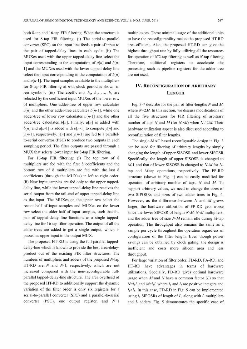
both 8-tap and 16-tap FIR filtering. When the structure is used for 8-tap FIR filtering: (i) The serial-to-parallel converter (SPC) on the input line feeds a pair of input to the pair of tapped-delay lines in each cycle. (ii) The MUXes used with the upper tapped-delay line select the input corresponding to the computation of a[n] and b[n-1] and the MUXes used with the lower tapped-delay line select the input corresponding to the computation of b[n] and a[n-1]. The input samples available to the multipliers for 8-tap FIR filtering at n-th clock period is shown in red symbols. (iii) The coefficients h0, h1, …, h7 are selected by the coefficient input MUXes of the lower row of multipliers. One adder-tree of upper row calculates a[n] and the other adder-tree calculates b[n-1], while one adder-tree of lower row calculates a[n-1] and the other adder-tree calculates b[n]. Finally, a[n] is added with b[n] and a[n-1] is added with b[n-1] to compute y[n] and y[n-1], respectively. y[n] and y[n-1] are fed to a parallel-to-serial convertor (PSC) to produce two outputs in each sampling period. The filter outputs are passed through a MUX that selects lower input for 8-tap FIR filtering.
For 16-tap FIR filtering: (i) The top row of 8 multipliers are fed with the first 8 coefficients and the bottom row of 8 multipliers are fed with the last 8 coefficients (through the MUXes) in left to right order. (ii) New input samples are fed only to the upper tapped-delay line, while the lower tapped-delay line receives the serial output from the tail-end of upper tapped-delay line as the input. The MUXes on the upper row select the recent half of input samples and MUXes on the lower row select the older half of input samples, such that the pair of tapped-delay line functions as a single tapped-delay line for 16-tap filter operation. The output of all the adder-trees are added to get a single output, which is passed as upper input to the output MUX.
The proposed HT-RD is using the full-parallel tapped-delay-line which is known to provide the best area-delay-product out of the existing FIR filter structures. The numbers of multipliers and adders of the proposed N-tap HT-RD are N and N-1, respectively, which are not increased compared with the non-reconfigurable full-parallel tapped-delay-line structure. The area overhead of the proposed HT-RD to additionally support the dynamic variation of the filter order is only six registers for a serial-to-parallel converter (SPC) and a parallel-to-serial converter (PSC), one output register, and N+1
multiplexors. These minimal usage of the additional units to have the reconfigurability makes the proposed HT-RD area-efficient. Also, the proposed HT-RD can give the highest throughput rate by fully utilizing all the resources for operation of N/2-tap filtering as well as N-tap filtering. Therefore, additional registers to accelerate the processing such as pipeline registers for the adder tree are not used.
IV. RECONFIGURATION OF ARBITRARY
LENGTH
Fig. 3-7 describe for the pair of filter-lengths N and M, where N=2M. In this section, we discuss modifications of all the five structures for FIR filtering of arbitrary number of taps N and M (for N>M) when N≠2M. Their hardware utilization aspect is also discussed according to reconfiguration of filter lengths.
The single-MAC based reconfigurable design in Fig. 3 can be used for filtering of arbitrary lengths by simply changing the length of upper SISOSR and lower SISOSR. Specifically, the length of upper SISOSR is changed to M-1 and that of lower SISOSR is changed to N-M for N-tap and M-tap operations, respectively. The FP-RD structure (shown in Fig. 4) can be easily modified for operation of arbitrary number of taps, N and M. To support arbitrary values, we need to change the sizes of two SIPOSRs and sizes of two adder trees in Fig. 4. However, as the difference between N and M grows larger, the hardware utilization of FP-RD gets worse since the lower SIPOSR of length N-M, N-M multipliers, and the adder tree of size N-M remain idle during M-tap operation. The throughput also remains the same as a sample per cycle throughout the operation regardless of configuration of the filter length. Even though power savings can be obtained by clock gating, the design is inefficient and costs more silicon area and less throughput.
For large variation of filter order, FD-RD, FA-RD, and HT-RD have advantages in terms of hardware utilizations. Specially, FD-RD gives optimal hardware usage when M and N have a common factor (L) so that N=l1L and M=l2L where l1 and l2 are positive integers and l1>l2. In this case, FD-RD in Fig. 5 can be implemented using l1 SIPOSRs of length of L, along with L multipliers and L adders. Fig. 5 demonstrates the specific case of

268 PRAMOD KUMAR MEHER et al : RECONFIGURABLE FIR FILTER FOR DYNAMIC VARIATION OF FILTER ORDER AND …
l1=2 and l2=1. If M and N do not have a common factor, the hardware elements which are not used need to be removed. For example, if N=37 and M=10, the value of L is set to 10 and the structure can be arranged in 4 rows (l1=4), each having SIPOSR of length 10 while the last three registers in the 4-th SIPOSR are removed. Another alternative is to arrange it in 8 rows (l1=8) so that each having SIPOSR of length 5 (L=5), which gives a different trade-off between the throughput and the silicon area. The structure of FA-RD in Fig. 6 is optimal in hardware usages when N=2M because it is based on two-parallel FIR algorithm. If N=mM where m is more than two, alternative structures can be derived using more number of parallel units. HT-RD has two delay lines as shown in Fig. 7, and both delay lines, all the multipliers, and adders are active during lower-order operation unlike FD-RD and FA-RD. HT-RD gives a better hardware utilization when N=mM and m is close to an integer so that most of hardware components remain active during the lower order operation.
V. HARDWARE AND TIME COMPLEXITY
1. Comparison of Theoretical Complexity Estimates Sampling periods of all the five reconfigurable
structures are listed in Table 1 when they are used for both N/2-tap and N-tap FIR filtering. When SM-RD is used for N-tap FIR filtering, the sample period becomes N×(TM+TA+TMX2+TR), where TM is duration of a non-pipelined multiplier used for multiplication of an input sample and a coefficient word, while TA, TMX2, and TR are delays of an adder, a 2:1 MUX, and a register,
respectively. Besides, the sample period for N/2-tap FIR filtering becomes half of that for N-tap FIR filtering. FP-RD can support the minimum sample period
(TM+ 2log Né ùê ú · TA+TMX2+TR) for N-tap operation, where
2log Né ùê ú ·TA is delay of 2log Né ùê ú -stage adder-tree for
the sum of products resulting from N-taps. Note that FP-RD provides the same throughput as well as the same minimum sample period for both N-tap and N/2-tap FIR filtering. The minimum sampling period supported by FD-RD is the same as that of FP-RD for N-tap operation whereas for N/2-tap operation, the sample period of FD-RD is the double that of FP-RD. The minimum sampling period of FA-RD for N/2-tap operation is slightly larger than the one of FP-RD as it involves a delay of 3:1 MUX instead of 2:1 MUX. The minimum sampling period of FA-RD for N-tap operation is 1.5 times longer than the one for N/2-tap operation. HT-RD can produce two consecutive outputs for N/2-tap filter or one output corresponding to N-tap filter in clock cycle. Therefore, it provides the shortest sampling period and the highest throughput rate for N/2-tap operation among all the listed structures.
The number of hardware elements such as multipliers (MULs), adders (ADDs), registers (REGs), and MUXes of reconfigurable FIR filter in Fig. 3-7 are listed in Table 2. SM-RD involves a multiplier, an adder, and 2N-1 registers for SISOSR, and another output register, and three 2:1 MUXes. FP-RD requires N multipliers, N-1 adders, N-1 registers for the input samples, N registers for the coefficients, and one final output register for full-parallel implementation of N-tap FIR filtering. FD-RD on the other hand requires almost half the area of FP-RD since FD-RD involves half the number of multipliers and
Table 1. Time complexities of different architectures for N/2-tap and N-tap FIR filtering
Sampling Period Design
(N/2)-tap FIR Filtering N-tap FIR Filtering
SM-RD 0.5N(TM+TA+TMX2+TR) N(TM+TA+TMX2+TR)
FP-RD TM+ 2log Né ùê ú ·TA+ TMX2+TR TM+ 2log Né ùê ú ·TA+ TMX2+TR
FD-RD TM+ 2log Né ùê ú ·TA+ TMX2+TR 2(TM+ 2log Né ùê ú ·TA+ TMX2+TR)
FA-RD TM+ 2log Né ùê ú ·TA+ TMX3+TR 1.5(TM+ 2log Né ùê ú ·TA+ TMX3+TR)
HT-RD 0.5(TM+ 2log Né ùê ú ·TA+ TMX2+TR) TM+ 2log Né ùê ú ·TA+ TMX2+TR
TM, TA, TMX2, TMX3, and TR are delays for a non-pipelined multiplier, an adder, a 2:1 MUX, and a 3:1 MUX, and a register, respectively.

JOURNAL OF SEMICONDUCTOR TECHNOLOGY AND SCIENCE, VOL.16, NO.3, JUNE, 2016 269
adders. But FD-RD requires additional N 2:1 MUXes to select corresponding input samples and coefficients for different option of lengths. FA-RD needs the same number of multipliers as FD-RD, but, needs more registers for input samples and coefficients, specifically, 3N/2 registers for SIPOSR, 3N/2 registers for coefficients, 4 registers for pre/processing block, and 1 output register. Also, it needs N 3:1 MUXes, and three 2:1 MUXes. Since the number of MUXes in Table 2 is based on 2:1 MUXes, a 3:1 MUX is replaced by 1.7 2:1 MUX considering the ratio of area of the two MUXes, and is listed in the Table. HT-RD has the same number of multipliers and adders as FP-RD, but includes more registers, specifically, N coefficient registers, N-1 input registers, 6 registers for SPC and PSC, and 1 output register.
2. Synthesis Results
We have coded all the five reconfigurable structures of
FIR filters for 16-bit coefficients, and 16-bit input by hardware description language (HDL) and synthesized by Synopsys Design Compiler using 90-nm CMOS
library which could be used for 16-tap and 8-tap FIR filters. Table 3 lists synthesis results including area, data-arrival-time (DAT),number of output samples per cycle (NOC), minimum sampling period (MSP), maximum sampling frequency (MSF), area-delay product (ADP), power consumption (PC) at 100 MHz operating clock, energy per sample (EPS), and energy delay product (EDP). We have not performed the truncation for the internal data across any of the designs in order to obtain output with maximum precision. SM-RD requires the least silicon area but the highest ADP, EPS, and EDP due to its long sample period. FP-RD requires the minimum EPS for 16-tap operation since it minimizes the usage of extra components for reconfigurability, but involves 62%, 23%, and 87% excess ADP over FD-RD, FA-RD, and HT-RD, respectively. FD-RD saves 40% of area over FP-RD, but supports MSF more than 100 MHz. Hence, FD-RD can be a candidate design option for applications requiring low-area with reasonably high throughput. FA-RD provides 24% area saving over FP-RD, and 29% higher MSF for 16-tap FIR filtering than FD-RD. HT-RD is found to have slightly more area than FP-RD, but offers almost double the MSF for 8-tap FIR filtering. HT-RD results in less ADP than all the other listed structures, therefore provides the best trade-off between area and time. Fig. 8 shows relative comparisons of four designs, FP-RD, FD-RD, FA-RD, and HT-RD in terms of average MSF, average ADP, and average EPS over 8-tap and 16-tap FIR filter operations. HT-RD provides almost 1.5 times higher throughput than FP-RD due to 49% higher average MSF at the cost of marginally increased EPS. In terms of average ADP, HT-RD offers
Table 2. Hardware complexities of reconfigurable FIR filters in Fig. 3-7
Number of Hardware Elements Design
MULs ADDs REGs 2:1 MUXes SM-RD 1 1 2N 3 FP-RD N N-1 2N 1 FD-RD 0.5N 0.5N 2N+1 N+1 FA-RD 0.5N 0.5N+3 3N+5 1.7N+3 HT-RD N N-1 2N+6 N+1
Table 3. Performance comparison of variable-length FIR filters based on synthesis results using 90-nm CMOS library
Design OP Area (um2)
DAT (ns) NOC MSP
(ns) MSF
(MHz) ADP
(um2×ns) PC
(mW) EPS
(mW×ns) EDP
(mW×ns2) 8 0.125 31.04 32.21 462092 1.13 90.84 2819.81
SM-RD 16
14887 3.38 0.062 62.08 16.10 924184 1.50 240.44 14926.63
8 1.92 19.27 90.79 FP-RD
16 77889 4.71 1 4.71 212.31 366857
3.67 36.77 173.22 8 1 4.92 203.25 226295 1.86 18.69 91.96
FD-RD 16
45995 4.92 0.5 9.84 101.62 452590 3.92 78.48 772.26
8 1 5.07 197.23 298050 1.50 15.07 76.42 FA-RD
16 58787 5.07
0.667 7.60 131.49 447052 5.17 77.59 590.07 8 2 2.38 421.05 195362 4.77 23.86 56.68
HT-RD 16
82258 4.75 1 4.75 210.52 390725 4.42 44.20 209.96
OP: operation of filtering, DAT: data arrival time, NOC: number of output samples per cycle, MSP: minimum sampling period, MSF: maximum sampling frequency, ADP: area-delay product, PC: power consumption at 100 MHz operating clock, EPS: energy per sample, EDP: energy delay product.

270 PRAMOD KUMAR MEHER et al : RECONFIGURABLE FIR FILTER FOR DYNAMIC VARIATION OF FILTER ORDER AND …
20% less ADP than FP-RD. FD-RD has less average ADP as well as less area than both FP-RD and FA-RD at the cost of higher MSF. FP-RD requires the minimum EPS, but involves 8% excess ADP over FD-RD and 25% excess ADP over HT-RD in average for 8-tap and 16-tap filter operations.
The proposed HT-RD is compared with the existing reconfigurable FIR filters [2, 7, 8, 23] and FIR filter in Synopsys Designware IP [27] in terms of silicon area and power consumption in Table 4. The existing designs have been simulated with different configurations of number of taps and wordlengths from simulations of the proposed designs. Also, they are using different operating clocks, supply voltages, and technology libraries. Therefore, it cannot be a fair comparison if we directly compare our simulation results with the ones reported in the reference papers. Therefore, in this paper, the normalized area consumption (Anorm) is used for a fair comparison which is represented as follows:
290 16 16 16 .
# # #normA AreaTech taps bits input bits coeffæ ö= ´ ´ ´ ´ç ÷è ø
(9)
Also, an equation in [28] is modified to normalize power consumption (Pnorm), and it is given by
2
90 16 16# #
16 100 1 .#
norm
DD
P Total PowerTech taps bits input
bits coeff clk freq V
= ´ ´ ´ ´
æ ö´ ´ç ÷
è ø
(10)
As shown in Table 4, the proposed HT-RD offers 80%
and 44% improvements in terms of normalized area and power consumptions over the best of existing designs [23] which support both reconfiguration of filter order and filter length.
Let us examine why the existing designs consume more area and power to add reconfigurability than the proposed design. Distributed-arithmetic (DA)-based FIR filters [7, 8] are known to be area-efficient. Also, DA-based structures can attain reconfigurability easily by updating the look-up-table (LUT). However, DA-based designs have a low throughput rate if the wordlength is large since it produces an output in every B cycles when the wordlength is B. Therefore, for high throughput applications, DA-based designs need many pipeline registers to reduce the critical-path, resulting in significant increases of area and power. Design of [2] is based on the canonical signed digit (CSD) requiring shift-add operation. Specially, [2] uses additional barrel shifters and carry save adders for reconfigurable shift-add operations which consume large area in the design.
(a) (b) (c)
Fig. 8. Comparison results of variable-length FIR filters in terms of (a) average maximum sampling frequency (MSF), (b) average area-delay product (ADP), (c) average energy per sample (EPS) over 8-tap and 16-tap filter operations.

JOURNAL OF SEMICONDUCTOR TECHNOLOGY AND SCIENCE, VOL.16, NO.3, JUNE, 2016 271
Design of [7] uses the systolic structure involving processing elements (PE) proportional to the number of taps and wordlength in order to have reconfigurability, and each PE involves a register requiring more area and power consumption than the proposed design.
Also, please note that the reference designs of [7, 8, 27] support only dynamic variations of filter coefficients not filter orders. The design of [23] can be configured to only two kinds of filter orders whereas the proposed approach can be configured to any filter order. The design of [2] also has run-time reconfigurabilities of the filter order and coefficients, but consumes more area and power than the proposed design.
VI. CONCLUSIONS
Reconfigurable FIR filter whose filter coefficients and filter order change dynamically during run-time are presented in this paper. We have derived five efficient structures for FIR filters which could be dynamically reconfigured to support different filter orders at the cost of different area and time complexity. From the synthesis results, it is found that the folded design occupies 40% less area than the full-parallel design, and the structure based on fast FIR algorithm provides 24% area saving over full-parallel design; and nearly 29% higher MSF for a higher order filtering than the folded design. The proposed high-throughput design offers almost double the speed at the cost of marginal increase in area compared to full-parallel structure, and also offers 80% less normalized area and 44% less normalized power consumption than the best of existing designs which support reconfiguration of filter order and filter length. The proposed designs can be applied to SDR systems offering reconfigurability as well as low power consumption.
ACKNOWLEDGMENT
This work was partially supported by the 2016 MPEES Advanced Research Center Fund of Myongji University.
REFERENCES
[1] T. Hentschel, M. Henker, and G. Fettweis, “The digital front-end of software radio terminals,” IEEE Personal Commun. Mag., vol. 6, no. 4, pp. 40–46, Aug. 1999.
[2] K.-H. Chen and T.-D. Chiueh, “A low-power digit-based reconfigurable FIR filter,” IEEE Trans. Circuits Syst. II, vol. 53, no. 8, pp. 617–621, Aug. 2006.
[3] L. Ming and Y. Chao, “The multiplexed structure of multi-channel FIR filter and its resources evaluation,” 2012 International Conference on Computer Distributed Control and Intelligent Environmental Monitoring (CDCIEM), Mar. 2012.
[4] I. Hatai, I. Chakrabarti, and S. Banerjee, “Reconfigurable architecture of a RRC FIR interpolator for multi-standard digital up converter,” Parallel and Distributed Processing Symposium Workshops PhD Forum (IPDPSW), IEEE 27th International, May, pp. 247–251.
[5] R. Mahesh and A. P. Vinod, “Low complexity flexible filter banks for uniform and non-uniform channelisation in software radios using coefficient decimation,” Circuits, Devices Systems, IET, vol. 5, no. 3, pp. 232–242, May 2011.
[6] E. Ozalevli, W. Huang, P. E. Hasler, and D. V. Anderson, “A reconfigurable mixed-signal VLSI implementation of distributed arithmetic used for finite-impulse response filtering,” IEEE Trans. Circuits Syst. I, vol. 55, no. 2, pp. 510–521, Mar.
Table 4. Comparison of the HT-RD with existing reconfigurable designs of FIR filters
Reference Method Tech (nm)
VDD (V)
Number of taps Bits Area
(mm2) Power (mW)
Clock (MHz)
Pnorm
(mW) Anorm
(mm2) [2] CSD 350 2.5 2.88 eqv. 8×8 2.8536 16.5 86 4.193 17.541
[7] DA-Systolic 90 1 16 8×8 0.0711 6.076 100 0.284 24.304
[8] DA 90 1 16 8×8 0.0251 1.303 100 0.100 5.212
[23] DA 90 1.1 64 12×19 1.5 130 380 0.421 7.936
[27] MAC 90 1 16 8×8 0.0519 1.363 100 0.207 5.452
Proposed HT-RD 90 1 16 16×16 0.0822 4.420 100 0.082 4.420

272 PRAMOD KUMAR MEHER et al : RECONFIGURABLE FIR FILTER FOR DYNAMIC VARIATION OF FILTER ORDER AND …
2008. [7] P. K. Meher, S. Chandrasekaran, and A. Amira,
“FPGA realization of FIR filters by efficient and flexible systolization using distributed arithmetic,” IEEE Trans. Signal Process., vol. 56, no. 7, pp. 3009–3017, Jul. 2008.
[8] S. Y. Park and P. K. Meher, “Efficient FPGA and ASIC realizations of DA-based reconfigurable FIR digital filter,” IEEE Trans. Circuits Syst. II, vol. 60, no. 7, pp. 511–515, Jul. 2014.
[9] M. Kumm, K. Moller, and P. Zipf, “Dynamically reconfigurable FIR filter architectures with fast reconfiguration,” Reconfigurable and Communica- tion-Centric Systems-on-Chip (ReCoSoC), 8th International Workshop on, Jul. 2013.
[10] M. Potkonjak, M. B. Srivastava, and A. P. Chandrakasan, “Multiple constant multiplications: efficient and versatile framework and algorithms for exploring common subexpression elimination,” IEEE Trans. Comput.-Aided Design Integr. Circuits Syst., vol. 15, no. 2, pp. 151–165, Feb. 1996.
[11] A. G. Dempster and M. D. Macleod, “Use of minimum-adder multiplier blocks in FIR digital filters,” IEEE Trans. Circuits Syst. II, vol. 42, no. 9, pp. 569–577, Sep. 1995.
[12] A. P. Vinod, A. Singla, and C. H. Chang, “Low-power differential coefficients-based FIR filters using hardware-optimised multipliers,” Circuits, Devices Systems, IET, vol. 1, no. 1, pp. 13–20, Feb. 2007.
[13] P. Tummeltshammer, J. C. Hoe, and M. Puschel, “Time-multiplexed multiple-constant multiplica- tion,” IEEE Trans. Comput.-Aided Design Integr. Circuits Syst., vol. 26, no. 9, pp. 1551–1563, Sep. 2007.
[14] R. Mahesh and A. P. Vinod, “New reconfigurable architectures for implementing FIR filters with low complexity,” IEEE Trans. Comput.-Aided Design Integr. Circuits Syst., vol. 29, no. 2, pp. 275–288, Feb. 2010.
[15] M. Faust, O. Gustafsson, and C.-H. Chang, “Reconfigurable multiple constant multiplication using minimum adder depth,” Signals, Systems and Computers (ASILOMAR), Conference Record of the Forty Fourth Asilomar Conference on, Nov. 2010, pp. 1297–1301.
[16] S.-F. Hsiao, J.-H. Z. Jian, and M.-C. Chen, “Low-cost FIR filter designs based on faithfully rounded truncated multiple constant multiplication/accumu- lation,” IEEE Trans. Circuits Syst. II, vol. 60, no. 5, pp. 287–291, May 2013.
[17] P. K. Meher and S. Y. Park, “Area-delay-power efficient fixed-point LMS adaptive filter with low adaptation-delay,” IEEE Trans. VLSI Syst., vol. 22, no. 2, pp. 362–371, Feb. 2014.
[18] ——, “Critical-path analysis and low-complexity implementation of LMS adaptive algorithm,” IEEE Trans. Circuits Syst. I, vol. 61, no. 3, pp. 778–788, Mar. 2014.
[19] ——, “High-throughput pipelined realization of adaptive FIR filter based on distributed arithmetic,” VLSI and System-on-Chip (VLSI-SoC), IEEE/IFIP 19th International Conference on, Oct. 2011, pp. 428–433.
[20] D. J. Allred, H. Yoo, V. Krishnan, W. Huang, and D. V. Anderson, “LMS adaptive filters using distributed arithmetic for high throughput,” IEEE Trans. Circuits Syst. I, vol. 52, no. 7, pp. 1327–1337, Jul. 2005.
[21] S. H. Yoon and M. H. Sunwoo, “An efficient variable-length tap FIR filter chip,” Design Automation Conference. Proceedings of the ASP-DAC ’98. Asia and South Pacific, Feb. 1998, pp. 157–161.
[22] S.-J. Lee, J.-W. Choi, S. W. Kim, and J. Park, “A reconfigurable FIR filter architecture to trade off filter performance for dynamic power consump- tion,” IEEE Trans. VLSI Syst., vol. 19, no. 12, pp. 2221–2228, Dec. 2011.
[23] F. Sheikh, M. Miller, B. Richards, D. Markovic, and B. Nikolic, “A 1-190Msamples/s 8-64 tap energyefficient reconfigurable FIR filter for multi-mode wireless communication,” Proc. 2010 IEEE Symposium on VLSI Circuits (VLSIC), Jun. 2010, pp. 207–208.
[24] K. K. Parhi, VLSI Digital Signal Procesing Systems: Design and Implementation. New York: John Wiley & Sons, Inc, 1999.
[25] J. G. Proakis and D. G. Manolakis, Digital Signal Processing: Principles, Algorithms and Applica- tions. Upper Saddle River, NJ: Prentice-Hall, 1996.
[26] D. A. Parker and K. K. Parhi, “Low-area/power parallel FIR digital filter implementations,” J. VLSI

JOURNAL OF SEMICONDUCTOR TECHNOLOGY AND SCIENCE, VOL.16, NO.3, JUNE, 2016 273
Signal Process. Syst., vol. 17, no. 1, 1997. [27] “Synposys, Inc., DesignWare Building Block IP
User Guide, 2012.06-SP2, Mountain View, CA.” [Online]. Available: http://www.synopsys.com/
[28] C. J. Nicol, P. Larsson, K. Azadet, and J. H. O’Neill, “A low-power 128-tap digital adaptive equalizer for broadband modems,” IEEE J. Solid-State Circuits, vol. 32, no. 11, pp. 1777–1789, Nov. 1997.
Pramod Kumar Meher received the B.Sc. (Honours) and M.Sc. degree in physics, and the Ph.D. degree in science from Sambalpur University, India, in 1976, 1978, and 1996, respectively. Currently, he is a Senior Research Scientist with Nanyang
Technological University, Singapore. Previously, he was a Professor of Computer Applications with Utkal University, India, from 1997 to 2002, and a Reader in electronics with Berhampur University, India, from 1993 to 1997. His research interest includes design of dedicated and reconfigurable architectures for computation-intensive algorithms pertaining to signal, image and video processing, communication, bio-informatics and intelligent computing. He has contributed more than 200 technical papers to various reputed journals and conference proceedings. Dr. Meher has served as a speaker for the Distinguished Lecturer Program (DLP) of IEEE Circuits Systems Society during 2011 and 2012 and Associate Editor of the IEEE TRANSACTIONS ON CIRCUITS AND SYSTEMS-II: EXPRESS BRIEFS during 2008 to 2011, IEEE TRANSACTIONS ON CIRCUITS AND SYSTEMS-I: REGULAR PAPERS during 2012-2013, IEEE TRANSACTIONS ON VERY LARGE SCALE INTEGRATION (VLSI) SYSTEMS from 2009-2014, and Integration - the VLSI Journal. Currently he is serving as the Associate Editor for the IEEE TRANSACTIONS ON CIRCUITS AND SYSTEMS FOR VIDEO TECHNOLOGY and the Journal of Circuits, Systems, and Signal Processing. Dr. Meher is a Fellow of the Institution of Electronics and Telecommuni- cation Engineers, India. He was the recipient of the Samanta Chandrasekhar Award for excellence in research in engineering and technology for 1999.
Sang Yoon Park received the B.S. degree in electrical engineering and the M.S. and Ph.D. degrees in electrical engineering and computer science from Seoul National Univer- sity, Seoul, Korea, in 2000, 2002, and 2006, respectively. He joined the
School of Electrical and Electronic Engineering, Nanyang Technological University, Singapore as a Research Fellow in 2007. From 2008 to 2014, he was a Research Scientist with Institute for Infocomm Research, Singapore. Since 2014, he has been an Assistant Professor with the Department of Electronic Engineering, Myongji University, Korea. His research interest includes design of dedicated and reconfigurable architectures for low-power and high-performance digital signal processing systems.