
Comprehensive Performance Analysis of Interconnect...
8
http://dx.doi.org/10.5573/JSTS.2014.14.6.824 JOURNAL OF SEMICONDUCTOR TECHNOLOGY AND SCIENCE, VOL.14, NO.6, DECEMBER, 2014 Manuscript received Sep. 18, 2014; accepted Oct. 29, 2014 Youngmin Kim, Jaemin Lee, and Myunghwan Ryu are with the School of Electrical and Computer Engineering, Ulsan National Institute of Science and Technology (UNIST), Ulsan, 689-798 Republic of Korea E-mail : [email protected] Comprehensive Performance Analysis of Interconnect Variation by Double and Triple Patterning Lithography Processes Youngmin Kim, Jaemin Lee, and Myunghwan Ryu Abstract—In this study, structural variations and overlay errors caused by multiple patterning lithography techniques to print narrow parallel metal interconnects are investigated. Resistance and capacitance parasitic of the six lines of parallel interconnects printed by double patterning lithography (DPL) and triple patterning lithography (TPL) are extracted from a field solver. Wide parameter variations both in DPL and TPL processes are analyzed to determine the impact on signal propagation. Simulations of 10% parameter variations in metal lines show delay variations up to 20% and 30% in DPL and TPL, respectively. Monte Carlo statistical analysis shows that the TPL process results in 21% larger standard variation in delay than the DPL process. Crosstalk simulations are conducted to analyze the dependency on the conditions of the neighboring wires. As expected, opposite signal transitions in the neighboring wires significantly degrade the speed of signal propagation, and the impact becomes larger in the C-worst metals patterned by the TPL process compared to those patterned by the DPL process. As a result, both DPL and TPL result in large variations in parasitic and delay. Therefore, an accurate understanding of variations in the interconnect parameters by multiple patterning lithography and adding proper margins in the circuit designs is necessary. Index Terms—Double Patterning Lithography (DPL), Triple Patterning Lithography (TPL), Litho-etch litho-etch (LELE), Multipatterning, Interconnect Variation, RC Delay I. INTRODUCTION As semiconductor technology advances toward sub- 20-nm nodes, the dimensions of the back end of line (BEOL) decrease according to the scaling of the device [1]. Thus, patterning of narrow interconnects has become a major bottleneck for the success of the manufacturing of integrated circuits (ICs). To resolve BEOL patterning problems, several pitch splitting techniques have been proposed and considered as efficient solutions [2-8]. Double patterning lithography (DPL), or litho-etch-litho-etch (LELE), has been used for 20-nm logic nodes to pattern interconnect dimensions less than 100 nm [4, 9, 10]. In the DPL process, the original design is decomposed into two separate masks (or colors), and then interconnect lines are printed by the two continuous litho-etch processes to print narrow lines reusing existing 193-nm and 1.35-NA lithography. Recently, the triple patterning lithography (TPL), or litho-etch-litho-etch-litho-etch (LELELE), has been proposed for backend patterning of a 14-nm node in which the minimum metal pitch can be below 50 nm [1, 5, 6, 11, 12]. In TPL, three individual layers or masks can be generated in a layout decomposition as a direct extension of DPT. Then, triple lithography and an etching process are conducted continuously to pattern
Transcript of Comprehensive Performance Analysis of Interconnect...

http://dx.doi.org/10.5573/JSTS.2014.14.6.824 JOURNAL OF SEMICONDUCTOR TECHNOLOGY AND SCIENCE, VOL.14, NO.6, DECEMBER, 2014
Manuscript received Sep. 18, 2014; accepted Oct. 29, 2014 Youngmin Kim, Jaemin Lee, and Myunghwan Ryu are with the School of Electrical and Computer Engineering, Ulsan National Institute of Science and Technology (UNIST), Ulsan, 689-798 Republic of Korea E-mail : [email protected]
Comprehensive Performance Analysis of Interconnect Variation by Double and Triple Patterning Lithography
Processes
Youngmin Kim, Jaemin Lee, and Myunghwan Ryu
Abstract—In this study, structural variations and overlay errors caused by multiple patterning lithography techniques to print narrow parallel metal interconnects are investigated. Resistance and capacitance parasitic of the six lines of parallel interconnects printed by double patterning lithography (DPL) and triple patterning lithography (TPL) are extracted from a field solver. Wide parameter variations both in DPL and TPL processes are analyzed to determine the impact on signal propagation. Simulations of 10% parameter variations in metal lines show delay variations up to 20% and 30% in DPL and TPL, respectively. Monte Carlo statistical analysis shows that the TPL process results in 21% larger standard variation in delay than the DPL process. Crosstalk simulations are conducted to analyze the dependency on the conditions of the neighboring wires. As expected, opposite signal transitions in the neighboring wires significantly degrade the speed of signal propagation, and the impact becomes larger in the C-worst metals patterned by the TPL process compared to those patterned by the DPL process. As a result, both DPL and TPL result in large variations in parasitic and delay. Therefore, an accurate understanding of variations in the interconnect parameters by multiple patterning lithography and adding proper margins in the circuit designs is necessary.
Index Terms—Double Patterning Lithography (DPL), Triple Patterning Lithography (TPL), Litho-etch litho-etch (LELE), Multipatterning, Interconnect Variation, RC Delay
I. INTRODUCTION
As semiconductor technology advances toward sub-20-nm nodes, the dimensions of the back end of line (BEOL) decrease according to the scaling of the device [1]. Thus, patterning of narrow interconnects has become a major bottleneck for the success of the manufacturing of integrated circuits (ICs).
To resolve BEOL patterning problems, several pitch splitting techniques have been proposed and considered as efficient solutions [2-8]. Double patterning lithography (DPL), or litho-etch-litho-etch (LELE), has been used for 20-nm logic nodes to pattern interconnect dimensions less than 100 nm [4, 9, 10]. In the DPL process, the original design is decomposed into two separate masks (or colors), and then interconnect lines are printed by the two continuous litho-etch processes to print narrow lines reusing existing 193-nm and 1.35-NA lithography.
Recently, the triple patterning lithography (TPL), or litho-etch-litho-etch-litho-etch (LELELE), has been proposed for backend patterning of a 14-nm node in which the minimum metal pitch can be below 50 nm [1, 5, 6, 11, 12]. In TPL, three individual layers or masks can be generated in a layout decomposition as a direct extension of DPT. Then, triple lithography and an etching process are conducted continuously to pattern
JOURNAL OF SEMICONDUCTOR TECHNOLOGY AND SCIENCE, VOL.14, NO.6, DECEMBER, 2014 825
dense interconnects. Both DPL and TPL are good solutions for printing
highly dense and tiny interconnects. However, there are several inherent side effects in multipatterning lithography. The critical dimension (CD), or metal width, or metal height (H) between two adjacent lines (or three parallel lines in TPL) vary as the result of two (or three) separate lithography and etching processes [13]. In addition, overlay (OL) errors occur because of the misalignment between two or three consecutive litho-etch processes [9, 14, 15]. The OL errors cause nonuniform spacing between neighboring interconnect lines and are attributed to the change in the coupling capacitance. As a result, electrical parameters such as resistance and capacitance may differ among identical parallel lines in the same layers. Thus, understanding of the performance impact of the structural variations and OL errors by multiple pattern lithography have become extremely important for the success of future integrated circuit designs.
In [10], errors in space between metal lines were analyzed in a memory device. The authors showed statistical analysis results in which OL and etch bias were
the most important factors in space variability. The performance impact of RC delay and coupling capacitance on local interconnects by several advanced patterning options such as LELE, spacer-defined double patterning (SDDP), and extreme ultraviolet (EUV) lithography were analyzed in [13]. In [14], the process impacts of various DPL strategies were investigated, and the authors proposed a methodology to minimize the OL. A full-chip-level comparison between OL error and interconnect variations by the DPL process has been conducted in [15]. The authors claimed that the OL error does not affect the coupling capacitance at different layers, but the coupling-induced delay variation can reach 13% in 45-nm technology. There is space variation up to 17% in 6-nm OL error in a 40-nm node. A compact model for delay variations by DPL was proposed in [16]. An analytical timing variation model with coupling capacitance change due to OL error in DPL was proposed in [17]. The authors claimed that delay variation up to 9.1% can occur, which can be minimized to only 2.7% by a well-decomposed structure. Different OL sources by DPL were investigated electrically in [18]. The authors provided guidelines for design parameters for determining OL budget requirements. Analytical resistance and capacitance variation models of an LELE double patterning process were proposed in [19] and overlay impact for design in DPL has been analyzed in [20]. However, the relative impact on the delay
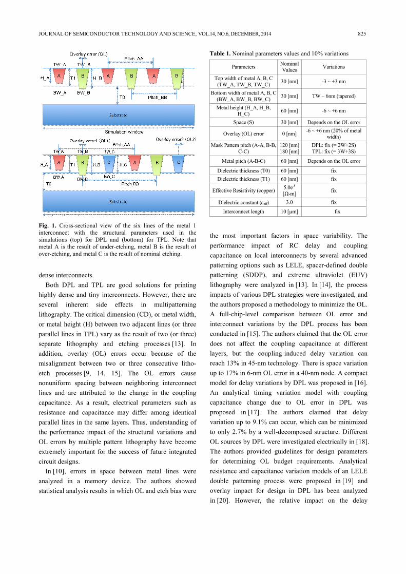
Fig. 1. Cross-sectional view of the six lines of the metal 1 interconnect with the structural parameters used in the simulations (top) for DPL and (bottom) for TPL. Note that metal A is the result of under-etching, metal B is the result of over-etching, and metal C is the result of nominal etching.
Table 1. Nominal parameters values and 10% variations
Parameters Nominal Values Variations
Top width of metal A, B, C (TW_A, TW_B, TW_C) 30 [nm] -3 ~ +3 nm
Bottom width of metal A, B, C (BW_A, BW_B, BW_C) 30 [nm] TW – 6nm (tapered)
Metal height (H_A, H_B, H_C) 60 [nm] -6 ~ +6 nm
Space (S) 30 [nm] Depends on the OL error
Overlay (OL) error 0 [nm] -6 ~ +6 nm (20% of metal width)
Mask Pattern pitch (A-A, B-B, C-C)
120 [nm] 180 [nm]
DPL: fix (= 2W+2S) TPL: fix (= 3W+3S)
Metal pitch (A-B-C) 60 [nm] Depends on the OL error
Dielectric thickness (T0) 60 [nm] fix Dielectric thickness (T1) 60 [nm] fix
Effective Resistivity (copper) 5.0e-8 [Ω-m] fix
Dielectric constant (eeff) 3.0 fix
Interconnect length 10 [µm] fix

826 YOUNGMIN KIM et al : COMPREHENSIVE PERFORMANCE ANALYSIS OF INTERCONNECT VARIATION BY DOUBLE AND …
variation between DPL and TPL in terms of the CD (with tapered cross-section), height variations, and OL error have not been investigated in the previous literature.
In this paper, structural variations (e.g., the width or height) in metals and OL errors of the DPL and TPL processes are combined and comprehensively evaluated, and the performance impacts of the variations are analyzed by the propagation delay of the interconnect. In addition, the crosstalk noise impact due to the coupling capacitance between neighboring wires is investigated.
The rest of this paper is organized as follows. Section II explains the simulation setup used in this study. Simulation results are discussed in Section III, followed by conclusions in Section IV.
II. SIMULATION SETUP
Six M1 interconnect lines are used to evaluate the CD and RC variations related to DPL and TPL as shown in Fig. 1. Metal dimensions and BEOL process techniques of the ITRS 22/20-nm technology node [1] are exploited, and the parameters are summarized in Table 1. The interconnect parasitic extraction tool Raphael [21] is used to extract the RC parameters of the metals as depicted in Fig. 2. We added drivers and receivers at two ends of the metal, which is 10 mm long. The propagation delay between the input of the driver and the input of the receiver is measured by Hspice [22] coupled with a 22-
nm high-performance predictive technology model (HP PTM) [23] as shown in Fig. 3.
We assume the damascene BEOL process with copper (Cu) metal, which is widely used in the patterning of advanced metallization. Unlike a lift-off process in Al, a Cu damascene process requires the etching of a trench first and then the depositing of Cu. As a result, the cross section of the metal assumes a trapezoidal shape rather than a rectangular shape [24-26]. Nonvertical sidewalls of metal conductors can usually be modeled with a nonzero sidewall or tapering angles [24, 25, 27]. For simplicity, the bottom width is set to 6 nm narrower than the top width of the metal (the tapering angle q is approximately 3o).
The DPL parameters and variation models of six lines of metal are shown in the top figure of Fig. 1. As observed in the figure, the neighboring metal lines are patterned by two different litho-etch processes (A and B). Therefore, the CD and height between metals A and B vary, and the OLs between them cause space variation.
The central metal A (i.e., the third metal from the left) is used to measure the propagation delay. The dimensional variation and OL cause significant variation in the capacitance and resistance of the metal line, which impacts the propagation delay.
The TPL parameters and variation models are described in the bottom figure of Fig. 1. As shown, three possible metallization processes can cause dimensional variations (i.e., CD and height of metal A, B, and C) and two OL errors (e.g., between A-B and A-C) among lines A, B, and C. In this case, the second metal A (i.e., the fourth metal from the left) is used to analyze the impact of the parasitic (R and C) and the propagation delay.
The testing circuit used to evaluate the performance impact of the RC variations caused by the DPL and TPL is shown in Fig. 3. One end of the extracted interconnect RC network is connected with an inverter driver, and the
Fig. 2. 2D graphical view of Raphael [21] input structures for RC extraction. The CD, height, and OL variations for the worst RC in DPL (top) and in TPL (bottom). The arrows indicate the E-field used in the field solver.
Fig. 3. Testing circuit to investigate the impact of the RC variations induced by double and triple pattering (10 µm line length is used with inverters of Wn = 50 nm and Wp = 75 nm).

JOURNAL OF SEMICONDUCTOR TECHNOLOGY AND SCIENCE, VOL.14, NO.6, DECEMBER, 2014 827
other end is connected to a receiver. The size of the inverter is Wn = 50 nm, and Wp = 1.5 x Wn. A pulse signal with a 100-ps rise/fall time is applied to the driver input, and the 50% propagation delay between the input of the driver and the input of the receiver (i.e., the end point of the metal) is measured.
III. SIMULATION RESULTS
1. Impact of 10% Parameter Variations At first, all parameters vary up to ±10% of the nominal
values with worst-case OL of up to ±6 nm which is the 20% of the minimum feature size [1]. The minimum and maximum capacitance, resistance, and propagation delay (Tp) are summarized in Table 2. The normalized R, C, and delay numbers are shown as well. As observed in the table, there is a higher capacitance change due to the multiple patterning process than due to the nominal patterning process. The total capacitance varies between -15% and +20% in DPL and between -22% and +35% in TPL. As a result of the capacitance and resistance changes, the propagation delay varies up to 20% (-9% ~ +11%) and 30% (-12% ~ +18%) by DPL and TPL, respectively. For example, in TPL, the delay will be 18% slower in the worst case and becomes 12% faster than the nominal delay in the best case when all dimensional parameters vary up to 10% from the nominal values. When we assume that there are no overlay errors both in DPL and TPL, the structural height and CD variation account for a delay penalty of up to 10% in the worst case. The worst-case ±6 nm OL leads to additional delay increases of approximately 1% and 7% on the
interconnects in DPL and TPL, respectively.
2. Impact of Overlay (OL) Error The OL variation is separately analyzed by fixing
other parameters to assess the capacitance effect from the space variation on the performance. The coupling (Cc), ground (Cg), total capacitance (Ct), and propagation delay variation by DPL-induced OL errors up to ±6 nm are plotted in Fig. 4. The capacitance change and delay variation by the TPL OL errors are shown in Figs. 5(a) and (b), respectively. There are two OL errors for metals B and C in TPL. As expected, the capacitance shows symmetric behavior for positive and negative OL errors because there are two neighboring interconnects (left and right), which move left and right together because of the OL error in DPL. Cg becomes smaller, and Cc becomes larger as the OL error increases from a perfect alignment. As a result, the total capacitance becomes 2.6% larger at the worst OL error which result in the 1% delay penalty.
On the other hand, there are two possible OL errors in the TPL (e.g., between metals A-B (OL1) and A-C (OL2)). The maximum capacitance variation occurs at OL1 = -6 nm and OL2 = +6 nm. This case makes sense in terms of the spacing between lines because the right line (litho-etch of the B metal) of the fourth metal line is closest at OL1 = -6 nm, and the left line (litho-etch of the C metal) of the fourth metal line is closest when OL2 = +6 nm. The minimum capacitive effect is expected when the opposite case (OL1 = +6 nm and OL2 = -6 nm) occurs. There is up to a 16% total capacitance increase due to the TPL-induced variation as shown in Fig. 5(a). The propagation delay results are
Table 2. Parasitic and delay change by parameter variations of 10%. In DPL, the minimum cap. and the minimum delay occurs when HA = HB = 54 nm and OL = 0, and the maximum cap. and the worst delay occurs when HA = HB = 66 nm and OL = 6 nm. In TPL, the minimum cap. and the minimum delay occurs when HA = HB = HC = 54 nm, OL1 = +6 nm, and OL2 = -6 nm, and the maximum cap. and the worst delay happens when HA = HB = HC = 66 nm, OL1 = -6 nm, and OL2 = +6 nm.
Ctotal (fF) R (KΩ) delay (ps) Patterning Process min nom. max min nom. max min nom. max
DPL 1.51 1.77 2.12 13.08 13.15 13.23 31.37 34.43 38.12 TPL 1.38 1.77 2.38 13.08 13.15 13.24 30.16 34.44 40.51
DPL (nor.) 0.85 1.00 1.20 0.99 1.00 1.01 0.91 1.00 1.11 TPL (nor.) 0.78 1.00 1.35 0.99 1.00 1.01 0.88 1.00 1.18
Fig. 4. Normalized variations by an OL in DPL in capacitance (Cc, Cg, and Ct) and propagation delay (Tp).
828 YOUNGMIN KIM et al : COMPREHENSIVE PERFORMANCE ANALYSIS OF INTERCONNECT VARIATION BY DOUBLE AND …
shown in Fig. 5(b). A delay increase up to 1% is expected at the worst OL in DPL but a delay penalty up to 7% occurs with the TPL process. This means that TPL is more susceptible to the OL errors due to the three different litho-etch processes. It is interesting that the delay always becomes worse as the OL increases in DPL, but up to a 5% increase in speed over perfect alignment occurs in signal transmission at the best OL case in TPL (i.e., spaces between third, fourth, and fifth metal lines become wider than nominal).
As mentioned in the previous analysis, the 10% dimensional variations (i.e., height and CD) account for up to a 10% increment in the propagation delay, and additional delay penalties of 1% and 7% occur because of the OL errors in DPL and TPL, respectively.
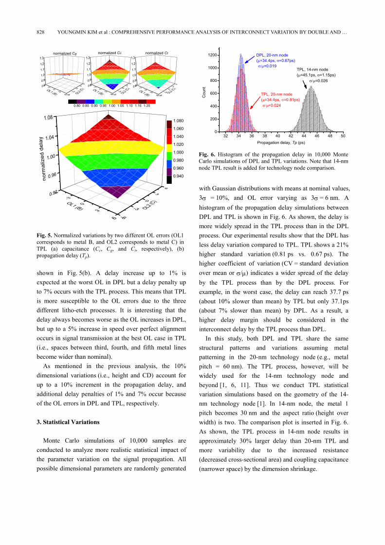
3. Statistical Variations
Monte Carlo simulations of 10,000 samples are
conducted to analyze more realistic statistical impact of the parameter variation on the signal propagation. All possible dimensional parameters are randomly generated
with Gaussian distributions with means at nominal values, 3s = 10%, and OL error varying as 3s = 6 nm. A histogram of the propagation delay simulations between DPL and TPL is shown in Fig. 6. As shown, the delay is more widely spread in the TPL process than in the DPL process. Our experimental results show that the DPL has less delay variation compared to TPL. TPL shows a 21% higher standard variation (0.81 ps vs. 0.67 ps). The higher coefficient of variation (CV = standard deviation over mean or s/m) indicates a wider spread of the delay by the TPL process than by the DPL process. For example, in the worst case, the delay can reach 37.7 ps (about 10% slower than mean) by TPL but only 37.1ps (about 7% slower than mean) by DPL. As a result, a higher delay margin should be considered in the interconnect delay by the TPL process than DPL.
In this study, both DPL and TPL share the same structural patterns and variations assuming metal patterning in the 20-nm technology node (e.g., metal pitch = 60 nm). The TPL process, however, will be widely used for the 14-nm technology node and beyond [1, 6, 11]. Thus we conduct TPL statistical variation simulations based on the geometry of the 14-nm technology node [1]. In 14-nm node, the metal 1 pitch becomes 30 nm and the aspect ratio (height over width) is two. The comparison plot is inserted in Fig. 6. As shown, the TPL process in 14-nm node results in approximately 30% larger delay than 20-nm TPL and more variability due to the increased resistance (decreased cross-sectional area) and coupling capacitance (narrower space) by the dimension shrinkage.
Fig. 5. Normalized variations by two different OL errors (OL1 corresponds to metal B, and OL2 corresponds to metal C) in TPL (a) capacitance (Cc, Cg, and Ct, respectively), (b) propagation delay (Tp).
Fig. 6. Histogram of the propagation delay in 10,000 Monte Carlo simulations of DPL and TPL variations. Note that 14-nm node TPL result is added for technology node comparison.
JOURNAL OF SEMICONDUCTOR TECHNOLOGY AND SCIENCE, VOL.14, NO.6, DECEMBER, 2014 829
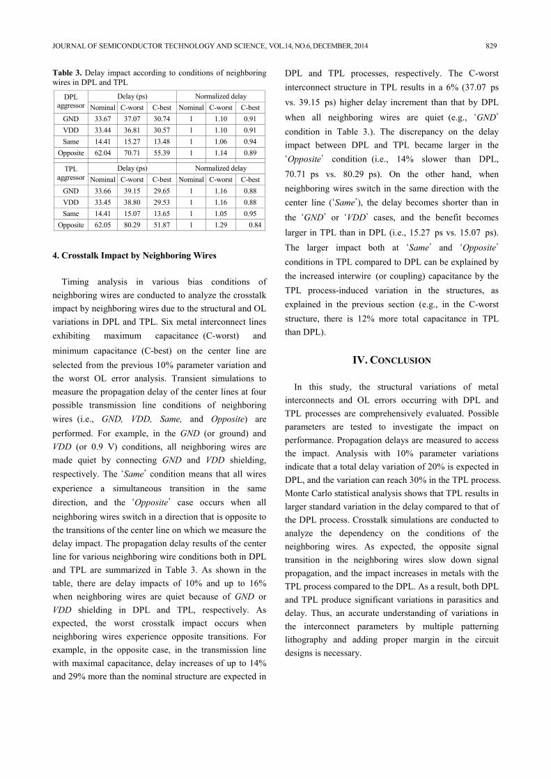
4. Crosstalk Impact by Neighboring Wires Timing analysis in various bias conditions of
neighboring wires are conducted to analyze the crosstalk impact by neighboring wires due to the structural and OL variations in DPL and TPL. Six metal interconnect lines exhibiting maximum capacitance (C-worst) and minimum capacitance (C-best) on the center line are selected from the previous 10% parameter variation and the worst OL error analysis. Transient simulations to measure the propagation delay of the center lines at four possible transmission line conditions of neighboring wires (i.e., GND, VDD, Same, and Opposite) are performed. For example, in the GND (or ground) and VDD (or 0.9 V) conditions, all neighboring wires are made quiet by connecting GND and VDD shielding, respectively. The ‘Same’ condition means that all wires experience a simultaneous transition in the same direction, and the ‘Opposite’ case occurs when all neighboring wires switch in a direction that is opposite to the transitions of the center line on which we measure the delay impact. The propagation delay results of the center line for various neighboring wire conditions both in DPL and TPL are summarized in Table 3. As shown in the table, there are delay impacts of 10% and up to 16% when neighboring wires are quiet because of GND or VDD shielding in DPL and TPL, respectively. As expected, the worst crosstalk impact occurs when neighboring wires experience opposite transitions. For example, in the opposite case, in the transmission line with maximal capacitance, delay increases of up to 14% and 29% more than the nominal structure are expected in
DPL and TPL processes, respectively. The C-worst interconnect structure in TPL results in a 6% (37.07 ps vs. 39.15 ps) higher delay increment than that by DPL when all neighboring wires are quiet (e.g., ‘GND’ condition in Table 3.). The discrepancy on the delay impact between DPL and TPL became larger in the ‘Opposite’ condition (i.e., 14% slower than DPL, 70.71 ps vs. 80.29 ps). On the other hand, when neighboring wires switch in the same direction with the center line (‘Same’), the delay becomes shorter than in the ‘GND’ or ‘VDD’ cases, and the benefit becomes larger in TPL than in DPL (i.e., 15.27 ps vs. 15.07 ps). The larger impact both at ‘Same’ and ‘Opposite’ conditions in TPL compared to DPL can be explained by the increased interwire (or coupling) capacitance by the TPL process-induced variation in the structures, as explained in the previous section (e.g., in the C-worst structure, there is 12% more total capacitance in TPL than DPL).
IV. CONCLUSION
In this study, the structural variations of metal interconnects and OL errors occurring with DPL and TPL processes are comprehensively evaluated. Possible parameters are tested to investigate the impact on performance. Propagation delays are measured to access the impact. Analysis with 10% parameter variations indicate that a total delay variation of 20% is expected in DPL, and the variation can reach 30% in the TPL process. Monte Carlo statistical analysis shows that TPL results in larger standard variation in the delay compared to that of the DPL process. Crosstalk simulations are conducted to analyze the dependency on the conditions of the neighboring wires. As expected, the opposite signal transition in the neighboring wires slow down signal propagation, and the impact increases in metals with the TPL process compared to the DPL. As a result, both DPL and TPL produce significant variations in parasitics and delay. Thus, an accurate understanding of variations in the interconnect parameters by multiple patterning lithography and adding proper margin in the circuit designs is necessary.
Table 3. Delay impact according to conditions of neighboring wires in DPL and TPL
Delay (ps) Normalized delay DPL aggressor Nominal C-worst C-best Nominal C-worst C-best
GND 33.67 37.07 30.74 1 1.10 0.91 VDD 33.44 36.81 30.57 1 1.10 0.91 Same 14.41 15.27 13.48 1 1.06 0.94
Opposite 62.04 70.71 55.39 1 1.14 0.89
Delay (ps) Normalized delay TPL aggressor Nominal C-worst C-best Nominal C-worst C-best
GND 33.66 39.15 29.65 1 1.16 0.88 VDD 33.45 38.80 29.53 1 1.16 0.88 Same 14.41 15.07 13.65 1 1.05 0.95
Opposite 62.05 80.29 51.87 1 1.29 0.84

830 YOUNGMIN KIM et al : COMPREHENSIVE PERFORMANCE ANALYSIS OF INTERCONNECT VARIATION BY DOUBLE AND …
REFERENCES
[1] International Technology Roadmap for Semicon- ductors (ITRS), [Online]. Available: http://www. itrs.net/Links/2013ITRS/Home2013.htm
[2] A. B. Kahng, C.-H. Park, X. Xu, and H. Yao, “Layout Decomposition Approaches for Double Patterning Lithography,” IEEE Transactions on CAD of Integrated Circuits and Systems, vol. 29, no. 6, pp. 939-952, 2010.
[3] K. Yuan, J. S. Yang, and D. Z. Pan, “Double Patterning Layout Decomposition for Simultaneous Conflict and Stitch Minimization,” IEEE Transactions on CAD of Integrated Circuits and Systems, vol. 29, no. 2, pp. 185-196, 2010.
[4] G. Luk-Pat, P. Panaite, K. Lucas, C. Cork, V. Wiaux, S. Verhaegen, and M. Maenhoudt, “Printability Verification for Double-Patterning Technology,” in Proc. of SPIE 7122, Photomask Technology, 2008.
[5] C. Cork, J.-C. Madre, and L. Barnes, “Comparison of Triple-Patterning Decomposition Algorithms Using Aperiodic Tiling Patterns,” in Proc. of SPIE 7028, Photomask and Next-Generation Lithography Mask Technology XV, vol. 7028, pp. 39.1-7, 2008.
[6] B. Yu, K. Yuan, B. Zhang, D. Ding, and D. Z. Pan, “Layout Decomposition for Triple Patterning Lithography,” in Proc. of ICCAD, pp. 1-8, 2011.
[7] Y. Ban, K. Lucas, and D. Pan, “Flexible 2D Layout Decomposition Framework for Spacer-Type Double Patterning Lithography,” in Proc. of Design Automation Conference (DAC), pp. 798-794, 2011.
[8] B. Yu, X. Xu, J.-R. Gao, and D. Pan, “Methodology for Standard Cell Compliance and Detailed Placement for Triple Patterning Lithography,” in Proc. of ICCAD, pp. 349-356, 2013.
[9] R. H. Kim, et al., “Double Exposure Using 193nm Negative Tone Photoresist,” in Proc. of SPIE Optical Microlithography XX, vol. 65202M, pp. 2M.1-8, 2007.
[10] A. Sezginer, B. Yenikaya, and W. Staud, “Double Patterning Technology: Process-Window Analysis in a Many-Dimensional Space,” in Proc. of Photomask and Next-Generation Lithography Mask Technology XIV, vol. 6607, pp. 2S.1-9, 2007.
[11] K. Lucas, et al., “Implications of Triple Patterning
for 14nm Node Design and Patterning,” in Proc. of SPIE 8327, Design for Manufacturability Through Design-Process Integration VI, vol. 8327, pp. 03.1-12, 2012.
[12] Q. Li, et al., “14nm M1 Triple Patterning,” in Proc. of SPIE 8326, Optical Microlithography XXV, vol. 8326, pp. 1-7, 2012.
[13] M. Stucchi, Z. Tòkei, S. Demuynck, and Y.-K. Siew, “Impact of Advanced Patterning Options, 193nm and EUV, on Local Interconnect Performance,” in Proc. of Interconnect Technology Conference (IITC), 2012 IEEE International, pp. 1-3, 2012.
[14] D. Laidler, et al, “Sources of Overlay Error in Double Patterning Integration Schemes,” in Proc. of SPIE Metrology, Inspection, and Process Control for Microlithography XXII, vol. 6922, pp. 1E.1-11, 2008.
[15] K. Jeong, A. B. Kahng, and R. O. Topaloglu, “Is Overlay Error More Important Than Interconnect Variations in Double Patterning?,” in Proc. of SLIP, pp. 3-10, 2009.
[16] E. Y. Chin and A. R. Neureuther, “Variability Aware Interconnect Timing Models for Double Patterning,” in Proc. of SPIE 7275, Design for Manufacturability Through Design-Process Integration III, vol. 7275, pp. 1-9, 2009.
[17] J.-S. Yang and D. Z. Pan, “Overlay Aware Interconnect and Timing Variation Modeling for Double Patterning Technology,” in Proc. Of ICCAD, pp. 488-493, 2008.
[18] R. S. Ghaida and P. Gupta, “Design-Overlay Interactions in Metal Double Patterning,” in Proc. of SPIE Design for Manufacturability Through Design-Process Integration III, vol. 7275, pp. 14.1-10, 2009.
[19] T.-B. Chan, K. Jeong, and A. B. Kahng, “Performance and Variability Driven Guidelines for BEOL Layout Decomposition with LELE Double Patterning,” in Proc. of SPIE 8166, Photomask Technology, vol. 8166, pp. 30.1-12, 2011.
[20] R. S. Ghaida and P. Gupta, “Within-Layer Overlay Impact for Design in Metal Double Patterning,” Semiconductor Manufacturing, IEEE Transactions on, vol. 23, no. 3, pp. 381-390, 2010.
[21] Raphael reference manual, ver. H-2013.03,

JOURNAL OF SEMICONDUCTOR TECHNOLOGY AND SCIENCE, VOL.14, NO.6, DECEMBER, 2014 831
[Online]. Available: http://www.synopsys.com. [22] Hspice reference manual, ver. H-2013.03-SP1,
[Online]. Available: http://www.synopsys.com. [23] 22nm PTM HP models, [Online]. Available:
http://ptm.asu.edu. [24] N. D. Arora, “Modeling and Characterization of
Copper Interconnects for SoC Design,” in Proc. of International Conference on Simulation of Semiconductor Processes and Devices, pp. 1-6, 2003.
[25] P. Gupta, et al., “Closing the Loop in Interconnect Analyses and Optimization: CMP Fill, Lithography and Timing,” in Proc. of International VLSI/ULSI Multilevel Interconnection Conference, pp. 352-363, 2005.
[26] J. Gambino, F. Chen, and J. He, “Copper Interconnect Technology for the 32 nm Node and Beyond,” in Proc. of IEEE Custom Integrated Circuits Conference, pp. 141-148, 2009.
[27] D. Sinha, J. Luo, S. Rajagopalan, and S. Batterywala, “Impact of Modern Process Technologies on the Electrical Parameters of Interconnects,” in Proc. of International Conference on VLSI Design, pp. 875-880, 2007.
Youngmin Kim received the B.S. degree in electrical engineering from the Yonsei University, Seoul, Korea, in 1999, and the M.S. and Ph.D. degrees in electrical engineering from the university of Michigan, Ann Arbor, in 2003 and 2007, respectively.
He has held a senior engineer position in the Qualcomm, San Diego, CA. He is currently an Assistant Professor in the school of electrical engineering and computer engineering at the Ulsan National Institute of Science and Technology (UNIST), Ulsan, South Korea. His research interests include variability-aware design methodologies, design for manufacturability, and design and technology co-optimization methodologies, and low-power and 3D IC designs.
Jaemin Lee received the B.S. degree of the multi-disciplinary majors of mechanical system design & manu- facturing and electrical engineering from Ulsan National Institute of Science and Technology (UNIST), Ulsan, Korea, in 2014. He is
currently in the M.S. program at Nano-scale Design & Automation Laboratory in school of electrical and computer engineering in UNIST. His research interests include low-power and high-performance circuit design, 3D TCAD modeling, and interconnect variation analysis and modeling.
Myunghwan Ryu received B.S. degree in electrical engineering an computer science from Kyungpook National University, Daegu, Korea, in 2010, and M.S. degree in electrical and computer engineering from the Ulsan National Institute of Science
and Technology (UNIST), Ulsan, Korea, in 2012, respectively, where he is currently working toward a Ph.D. degree in electrical engineering. His current research interests include TCAD-based compact modeling development for nano-scale CMOS/FinFETs, and Design Technology Co-Optimization methodologies, and design, simulation, modeling for variability of various emerging devices.


![High-Throughput Low-Complexity Successive- Cancellation ...jsts.org/html/journal/journal_files/2015/06/Year... · The list SC decoder from A. Balatsoukas-Stimming et al. [14] shows](https://static.fdocuments.in/doc/165x107/5f8bd2f29292176e317a0c60/high-throughput-low-complexity-successive-cancellation-jstsorghtmljournaljournalfiles201506year.jpg)


