Single-ended Differential RF Circuit Topologies Utilizing...
12
JOURNAL OF SEMICONDUCTOR TECHNOLOGY AND SCIENCE, VOL.2, NO. 1, MARCH, 2002 7 Single-ended Differential RF Circuit Topologies Utilizing Complementary MOS Devices Bonkee Kim, Ilku Nam, and Kwyro Lee Abstract − Single-ended differential RF circuit topologies fully utilizing complementary characteristics of both NMOS and PMOS are proposed, which have inherent advantage of both single-ended and differential circuits. Using this concept, we propose a CCPP (Complementary CMOS parallel push-pull) amplifier which has single-ended input/output with differential amplifying characteristics, leading to more than 30 dB improvement on IIP 2 . In addition, complementary resistive mixer is also proposed, which provides not only differential IF outputs from single-ended RF input, but much better linearity as well as isolation characteristics. Experimental results using 0.35 µm CMOS process show that, compared with conventional NMOS resistive mixer, the proposed mixer shows 15 dB better LO-to-IF isolation, 4.6 dB better IIP 2 , and 4.5 dB better IIP 3 performances. Index Terms − Single-ended, differential, RF, comple- mentary, MOS I. INTRODUCTION By virtue of continuous advances in fabrication technologies [1] – [3], CMOS is now ready to proceed to the sea of wireless RF market. Recent reports on CMOS RF circuits and systems show that it has performances good enough to be applied to 1 – 3 GHz applications such as GSM (Global System for Mobile communica- tions), PCS (Personal Communication Services), bluetooth, GPS (Global Positioning System), etc. Moreover, there are some reports even for 5 GHz band WLAN (Wireless Local Area Network) application [4] – [6]. Until now, the leading application for wireless communication market has been for mobile cellular phones, which are GSM for Europe and CDMA for U.S. and Korea, etc. In these systems, mobile users communicate with base stations, which are several kilometers away from them. Because of signal attenuation, power amplifiers and LNA (low noise amplifier) specifications are relatively tight for these applications. Large output power (~ 28 dBm for CDMA and ~ 33dBm for GSM) with high linearity is required for power amplifier, and low noise figure (less than 1.5 dB typically) is required for LNA. Low power consumption is mandatory for both receiver and transmitter. Because of these tight specifications, transceiver IC designers have been choosing the best- performance fabrication technology, such as GaAs MESFET, Si bipolar, and SiGe bipolar rather than low cost technology like CMOS. However, the situations for short-range communica- tion such as bluetooth, HomeRF and WLAN are definitely different from that of cellular phone. In these applications, a mobile user communicates with indoor devices, and the distances between them are normally within 100 m. In other words, much higher noise figure for receiver and much lower output power for transmitter can be accepted. For these applications, low cost and low power consumption are the first consideration factors. Manuscript received January 30, 2002; revised March 25, 2002. RF Products, System LSI business, Semiconductor, Samsung Electronics, Suwon P.O.Box 105, Kyunggi do, Korea. Department of Electrical Engineering and Computer Science, Korea Advanced Institute of Science and Technology, 373-1, Kusong dong, Yusong ku, Taejon, 305-701, Republic of Korea. (e-mail : [email protected]) Tel : +82-42 869 5462 Fax : +82 42 869 8530
Transcript of Single-ended Differential RF Circuit Topologies Utilizing...
JOURNAL OF SEMICONDUCTOR TECHNOLOGY AND SCIENCE, VOL.2, NO. 1, MARCH, 2002
7
Single-ended Differential RF Circuit Topologies Utilizing Complementary MOS Devices
Bonkee Kim, Ilku Nam, and Kwyro Lee
Abstract− Single-ended differential RF circuit topologies fully utilizing complementary characteristics of both NMOS and PMOS are proposed, which have inherent advantage of both single-ended and differential circuits. Using this concept, we propose a CCPP (Complementary CMOS parallel push-pull) amplifier which has single-ended input/output with differential amplifying characteristics, leading to more than 30 dB improvement on IIP2. In addition, complementary resistive mixer is also proposed, which provides not only differential IF outputs from single-ended RF input, but much better linearity as well as isolation characteristics. Experimental results using 0.35 µm CMOS process show that, compared with conventional NMOS resistive mixer, the proposed mixer shows 15 dB better LO-to-IF isolation, 4.6 dB better IIP2, and 4.5 dB better IIP3 performances.
Index Terms −Single-ended, differential, RF, comple-mentary, MOS
I. INTRODUCTION
By virtue of continuous advances in fabrication technologies [1] – [3], CMOS is now ready to proceed to
the sea of wireless RF market. Recent reports on CMOS RF circuits and systems show that it has performances good enough to be applied to 1 – 3 GHz applications such as GSM (Global System for Mobile communica-tions), PCS (Personal Communication Services), bluetooth, GPS (Global Positioning System), etc. Moreover, there are some reports even for 5 GHz band WLAN (Wireless Local Area Network) application [4] – [6].
Until now, the leading application for wireless communication market has been for mobile cellular phones, which are GSM for Europe and CDMA for U.S. and Korea, etc. In these systems, mobile users communicate with base stations, which are several kilometers away from them. Because of signal attenuation, power amplifiers and LNA (low noise amplifier) specifications are relatively tight for these applications. Large output power (~ 28 dBm for CDMA and ~ 33dBm for GSM) with high linearity is required for power amplifier, and low noise figure (less than 1.5 dB typically) is required for LNA. Low power consumption is mandatory for both receiver and transmitter. Because of these tight specifications, transceiver IC designers have been choosing the best-performance fabrication technology, such as GaAs MESFET, Si bipolar, and SiGe bipolar rather than low cost technology like CMOS.
However, the situations for short-range communica-tion such as bluetooth, HomeRF and WLAN are definitely different from that of cellular phone. In these applications, a mobile user communicates with indoor devices, and the distances between them are normally within 100 m. In other words, much higher noise figure for receiver and much lower output power for transmitter can be accepted. For these applications, low cost and low power consumption are the first consideration factors.
Manuscript received January 30, 2002; revised March 25, 2002. RF Products, System LSI business, Semiconductor, Samsung
Electronics, Suwon P.O.Box 105, Kyunggi do, Korea. Department of Electrical Engineering and Computer Science, Korea
Advanced Institute of Science and Technology, 373-1, Kusong dong, Yusong ku, Taejon, 305-701, Republic of Korea. (e-mail : [email protected]) Tel : +82-42 869 5462 Fax : +82 42 869 8530
B. KIM et al. : SINGLE-ENDED DIFFERENTIAL RF CIRCUIT TOPOLOGIES UTILIZING COMPLEMENTARY MOS DEVICES 8
CMOS is attractive for these short-range communication in that it is much cheaper than SiGe or GaAs process, and moreover, it can integrate digital modem part together in one-chip. This is the reason why most bluetooth and WLAN transceiver chips are designed and fabricated with CMOS process nowadays [4], [5], [7]. Moreover, there is some effort to integrate full CMOS RF transceiver even for high performance mobile cellular application like GSM [8]. In summary, CMOS RF IC’s are now rushing out of academic institutes into battlefield of RF markets.
Together with process technology selection, system architecture is another issue for recent wireless receiver design. Until now, almost all of wireless receiver adopted heterodyne architecture because of its high sensitivity and selectivity. Heterodyne is the best-performance architecture at the cost of large-volume, high-power, high-cost SAW filters and image rejection filters. Recently, IC designers have investigated direct conversion receiver (DCR) and low-IF architectures to remove large-volume and high-cost filters, some of which show performance comparable to that of conventional ones [9] – [13].
In DCR and low-IF receivers, because IF is DC or near DC, not only odd order nonlinearity, but also even order nonlinearity has significant effects on total nonlinearity [14]. In other words, IP2 (second order intercept point) as much as IP3 (third order intercept point) is an important specification for a receiver, and because of this reason, most direct conversion and low-IF receiver adopt fully differential signal structure, where even order nonlinearities can be canceled out. However, it requires large-volume baluns, which connect single-ended antenna to differential input stage in front RF circuits. Usually, baluns are implemented using large-size off-chip inductors and capacitors, which results in narrow band characteristics. Although wideband baluns can be implemented using resistors, it is not desirable because these low-Q elements increase signal loss and noise figure. These problems will be discussed further in section II and III.
In this paper, we propose several amplifier and mixer circuits for wireless RF application that fully utilize CMOS devices, i.e., both NMOS and PMOS. The complementary nature of these circuits inherently provides single-ended differential signal processing
capability, alleviating the use of baluns, or, differential signal generating circuits. One good example is the static CMOS digital logic circuit, which is undoubtedly one of best complementary circuits ever invented. Push-pull drive amplifier consisting of NMOS and PMOS source followers is another example.
Previous efforts to fully utilize CMOS RF circuits will be reviewed in Sec. II. Sec III describes characteristic features of complementary circuits specifically for RF applications, followed by some amplifier and mixer application examples in Sec. IV. Sec. V demonstrates experimental results for the proposed circuits in Sec. IV, followed by conclusion.
II. REVIEW OF PREVIOUS WORKS
As mentioned above, there have been many efforts on RF building blocks [15], [16], receivers [17], [18] and transceivers [19], [20], implemented using recent CMOS technologies. However, most of the RF core circuits consist only of NMOS, and PMOS is just used in bias circuits. This is quite in contrast with digital world where full utilization of complementary characteristics of CMOS leads to extremely low power and high-speed digital circuits and systems. High speed is due to shorter gate length and low parasitics, and low power is mainly due to complementary characteristics of NMOS and PMOS.
As mentioned above, in RF world, there are many technologies such as BJT, HBT, MESFET, HFET, etc., competing with each other. Among these, CMOS is the only viable technology in providing true complementary performance at RF, that is, although PMOS has lower ft and fmax than NMOS, the values are still well above 10 GHz [1], and that is enough to be used in 1 ~ 3 GHz application. In other words, complementary characteristics of NMOS and PMOS can indeed be fully utilized in RF core circuits without significant RF performance degradation.
Actually, there were several efforts to use PMOS as RF core circuit element. For example, PMOS cross-coupled pair that generates negative resistance for VCO was used to utilize its low phase noise characteristics [21]. They obtained phase noise of –128.5 dBc/Hz at 600 kHz offset from 2.05 GHz center frequency.
JOURNAL OF SEMICONDUCTOR TECHNOLOGY AND SCIENCE, VOL.2, NO. 1, MARCH, 2002
9
The use of both NMOS and PMOS was first adopted in VCO [22-25], where negative resistance generation circuits consisting of NMOS cross-coupled pair stacked with PMOS cross-coupled pair rather than NMOS-only or PMOS-only pair can lead to less power consumption. According to the analysis in [25], complementary and symmetric characteristics of NMOS and PMOS gives additional benefit of suppressing phase noise of RF oscillator. This is a good example of the use of complementary characteristics of NMOS and PMOS in RF analog circuit. Other examples include the power amplifier circuits [26] - [28], where PMOS is used as an active load to replace large size inductor load.
III. SINGLE-ENDED DIFFERENTIAL RF SIGNAL PROCESSING METHODS USING
COMPLEMENTARY DEVICES
In analog/digital circuits, signal lines are constructed with either single-ended or differential. Single-ended topology has advantages of simpler structure, smaller DC power consumption, lower noise figure, etc. On the other hand, differential topology provides inherent immunity to signal interference, as well as generates much less electromagnetic interference signal. Moreover, by virtue of symmetrical characteristics, it can eliminate even-order distortions. The former characteristics is important in integrating various mixed mode circuit blocks in one chip, and in implementing mixer which requires high isolation among RF, LO, and IF ports. The latter feature is important in implementing amplifier or mixer that require even order suppression. As discussed earlier, modern direct conversion receiver has stringent specification on 2nd order non-linearity because of its DC offset problem. Moreover, in power-efficient class B or class AB mode operation, single ended structure has a problem that the signal could be clamped which results in generation of large amount of harmonic components. Thus differential circuits are quite preferred.
One of the obstacles for differential scheme is that baluns are required to convert single-ended signal to differential inputs. Generally, baluns are large and heavy, difficult to integrate on chip in the case of passive implementation. In active version, it requires DC power consumption as well as its accuracy is not as good as
passive ones. Therefore, in current RF applications, differential core is integrated on-chip, and passive baluns are implemented on PCB using discrete passive elements, which are large and heavy. Passive baluns also require more time and labor in mass production.
Ps Nd
Input
Ns Pd
Bias &
matching
network
Bias &
matching
network
Bias &
matching
network
Vin
Idn
Idp
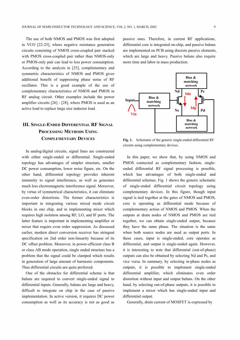
Fig. 1. Schematic of the generic single-ended differential RF circuits using complementary devices.
In this paper, we show that, by using NMOS and
PMOS connected as complementary fashion, single-ended differential RF signal processing is possible, which has advantages of both single-ended and differential schemes. Fig. 1 shows the generic schematic of single-ended differential circuit topology using complementary devices. In this figure, though input signal is tied together at the gates of NMOS and PMOS, core is operating as differential mode because of complementary action of NMOS and PMOS. When the outputs at drain nodes of NMOS and PMOS are tied together, we can obtain single-ended output, because they have the same phase. The situation is the same when both source nodes are used as output ports. In these cases, input is single-ended, core operates as differential, and output is single-ended again. However, it is interesting to note that differential (out-of-phase) outputs can also be obtained by selecting Nd and Ps, and vice versa. In summary, by selecting in-phase nodes as outputs, it is possible to implement single-ended differential amplifier, which eliminates even order distortion without input and output baluns. On the other hand, by selecting out-of-phase outputs, it is possible to implement a mixer which has single-ended input and differential output.
Generally, drain current of MOSFET is expressed by
B. KIM et al. : SINGLE-ENDED DIFFERENTIAL RF CIRCUIT TOPOLOGIES UTILIZING COMPLEMENTARY MOS DEVICES 10
-2 -1 0 1 2-90
-60
-30
0
30
60
90
PM OS
NM OSIds
(mA
)
Vgs (V) (a)
-2 -1 0 1 20
30
60
90
P M O S N M O S
g m (
mA
/V)
V gs (V )
(b)
-2 -1 0 1 2-200
-100
0
100
200
PMOS
NMOSg m' (
mA
/V2 )
Vgs (V) (c)
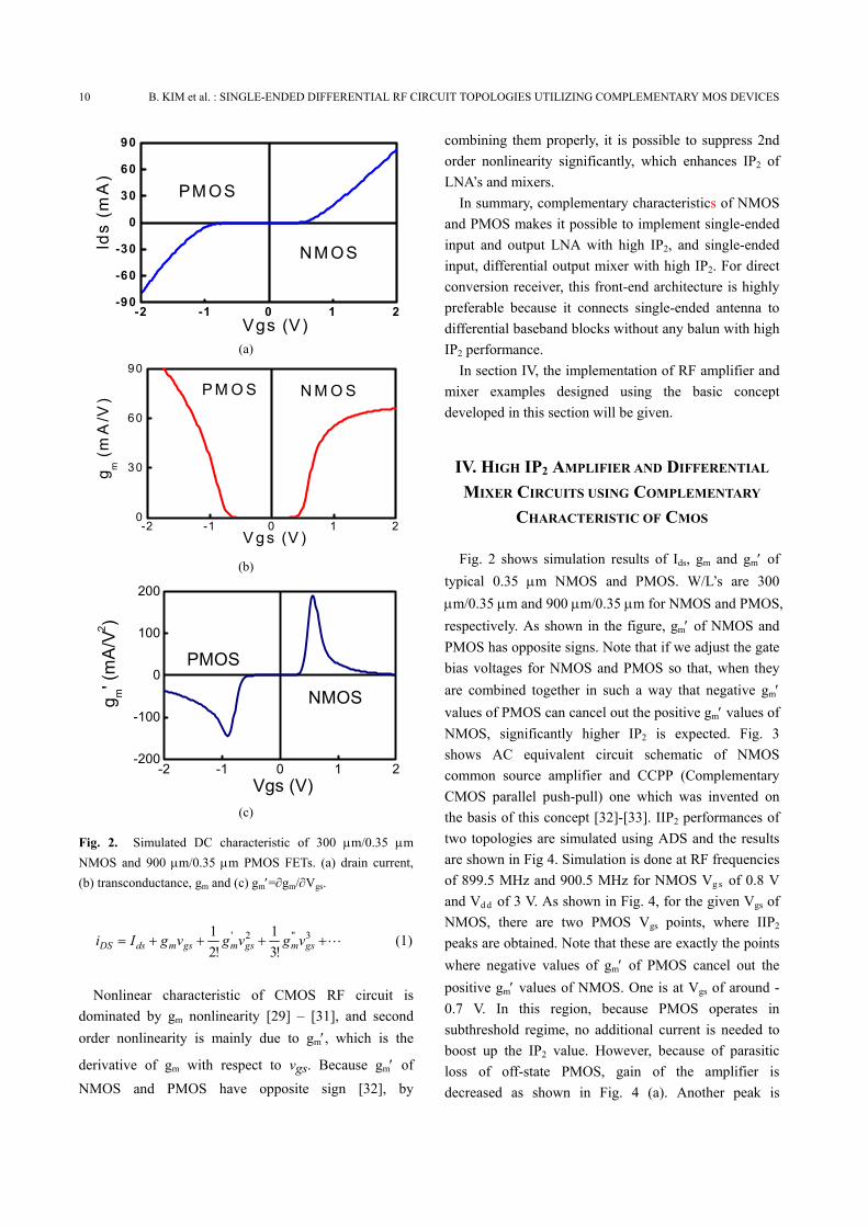
Fig. 2. Simulated DC characteristic of 300 µm/0.35 µm NMOS and 900 µm/0.35 µm PMOS FETs. (a) drain current, (b) transconductance, gm and (c) gm′=∂gm/∂Vgs.
⋅⋅⋅++++= 3"2'
!31
!21
gsmgsmgsmdsDS vgvgvgIi (1)
Nonlinear characteristic of CMOS RF circuit is
dominated by gm nonlinearity [29] – [31], and second order nonlinearity is mainly due to gm′, which is the
derivative of gm with respect to vgs. Because gm′ of NMOS and PMOS have opposite sign [32], by
combining them properly, it is possible to suppress 2nd order nonlinearity significantly, which enhances IP2 of LNA’s and mixers.
In summary, complementary characteristics of NMOS and PMOS makes it possible to implement single-ended input and output LNA with high IP2, and single-ended input, differential output mixer with high IP2. For direct conversion receiver, this front-end architecture is highly preferable because it connects single-ended antenna to differential baseband blocks without any balun with high IP2 performance.
In section IV, the implementation of RF amplifier and mixer examples designed using the basic concept developed in this section will be given.
IV. HIGH IP2 AMPLIFIER AND DIFFERENTIAL MIXER CIRCUITS USING COMPLEMENTARY
CHARACTERISTIC OF CMOS
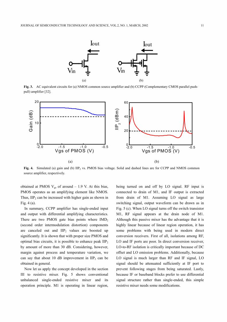
Fig. 2 shows simulation results of Ids, gm and gm′ of typical 0.35 µm NMOS and PMOS. W/L’s are 300 µm/0.35 µm and 900 µm/0.35 µm for NMOS and PMOS, respectively. As shown in the figure, gm′ of NMOS and PMOS has opposite signs. Note that if we adjust the gate bias voltages for NMOS and PMOS so that, when they are combined together in such a way that negative gm′ values of PMOS can cancel out the positive gm′ values of NMOS, significantly higher IP2 is expected. Fig. 3 shows AC equivalent circuit schematic of NMOS common source amplifier and CCPP (Complementary CMOS parallel push-pull) one which was invented on the basis of this concept [32]-[33]. IIP2 performances of two topologies are simulated using ADS and the results are shown in Fig 4. Simulation is done at RF frequencies of 899.5 MHz and 900.5 MHz for NMOS Vg s of 0.8 V and Vd d of 3 V. As shown in Fig. 4, for the given Vgs of NMOS, there are two PMOS Vgs points, where IIP2 peaks are obtained. Note that these are exactly the points where negative values of gm′ of PMOS cancel out the positive gm′ values of NMOS. One is at Vgs of around - 0.7 V. In this region, because PMOS operates in subthreshold regime, no additional current is needed to boost up the IP2 value. However, because of parasitic loss of off-state PMOS, gain of the amplifier is decreased as shown in Fig. 4 (a). Another peak is
JOURNAL OF SEMICONDUCTOR TECHNOLOGY AND SCIENCE, VOL.2, NO. 1, MARCH, 2002
11
Vin
Iout
Vin
Iout
(a) (b)
Fig. 3. AC equivalent circuits for (a) NMOS common source amplifier and (b) CCPP (Complementary CMOS parallel push-pull) amplifier [32].
-2.0 -1.5 -1.0 -0.50
10
20
Gai
n (d
B)
Vgs of PMOS (V)
-2.0 -1.5 -1.0 -0.50
20
40
60
IIP2 (d
Bm
)
Vgs of PMOS (V)
(a) (b)
Fig. 4. Simulated (a) gain and (b) IIP2 vs. PMOS bias voltage. Solid and dashed lines are for CCPP and NMOS commonsource amplifier, respectively.
obtained at PMOS Vgs of around – 1.9 V. At this bias, PMOS operates as an amplifying element like NMOS. Thus, IIP2 can be increased with higher gain as shown in Fig. 4 (a).
In summary, CCPP amplifier has single-ended input and output with differential amplifying characteristics. There are two PMOS gate bias points where IMD2 (second order intermodulation distortion) components are canceled out and IIP2 values are boosted up significantly. It is shown that with proper size PMOS and optimal bias circuits, it is possible to enhance peak IIP2 by amount of more than 30 dB. Considering, however, margin against process and temperature variation, we can say that about 10 dB improvement in IIP2 can be obtained in general.
Now let us apply the concept developed in the section III to resistive mixer. Fig. 5 shows conventional unbalanced single-ended resistive mixer and its operation principle. M1 is operating in linear region,
being turned on and off by LO signal. RF input is connected to drain of M1, and IF output is extracted from drain of M1. Assuming LO signal as large switching signal, output waveform can be drawn as in Fig. 5 (c). When LO signal turns off the switch transistor M1, RF signal appears at the drain node of M1. Although this passive mixer has the advantage that it is highly linear because of linear region operation, it has some problems with being used in modern direct conversion receivers. First of all, isolations among RF, LO and IF ports are poor. In direct conversion receiver, LO-to-RF isolation is critically important because of DC offset and LO emission problems. Additionally, because LO signal is much larger than RF and IF signal, LO signal should be attenuated sufficiently at IF port to prevent following stages from being saturated. Lastly, because IF or baseband blocks prefer to use differential signal structure rather than single-ended, this simple resistive mixer needs some modifications.
B. KIM et al. : SINGLE-ENDED DIFFERENTIAL RF CIRCUIT TOPOLOGIES UTILIZING COMPLEMENTARY MOS DEVICES 12
RF
LO
IF
RF
LO
IF
M1
(a) (b)
RF
LO
IF (c)
Fig. 5. (a) schematic, (b) symbol, and (c) waveforms for unbalanced single-ended NMOS resistive mixer.
RF
+ LO
+ IF
RF
LO
IF RF
- LO
- IF
A B
M1 M2 (a) (b)
RF
LO
A-B
(c)
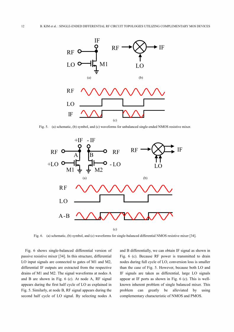
Fig. 6. (a) schematic, (b) symbol, and (c) waveforms for single-balanced differential NMOS resistive mixer [34].
Fig. 6 shows single-balanced differential version of passive resistive mixer [34]. In this structure, differential LO input signals are connected to gates of M1 and M2, differential IF outputs are extracted from the respective drains of M1 and M2. The signal waveforms at nodes A and B are shown in Fig. 6 (c). At node A, RF signal appears during the first half cycle of LO as explained in Fig. 5. Similarly, at node B, RF signal appears during the second half cycle of LO signal. By selecting nodes A
and B differentially, we can obtain IF signal as shown in Fig. 6 (c). Because RF power is transmitted to drain nodes during full cycle of LO, conversion loss is smaller than the case of Fig. 5. However, because both LO and IF signals are taken as differential, large LO signals appear at IF ports as shown in Fig. 6 (c). This is well-known inherent problem of single balanced mixer. This problem can greatly be alleviated by using complementary characteristic of NMOS and PMOS.
JOURNAL OF SEMICONDUCTOR TECHNOLOGY AND SCIENCE, VOL.2, NO. 1, MARCH, 2002
13
FicostfrN
RF
LO
IF RF
LO
+ IF
RF
LO
- IF
A B
M1 M2
(a) (b)
R F
L O
A
B
A - B (c)
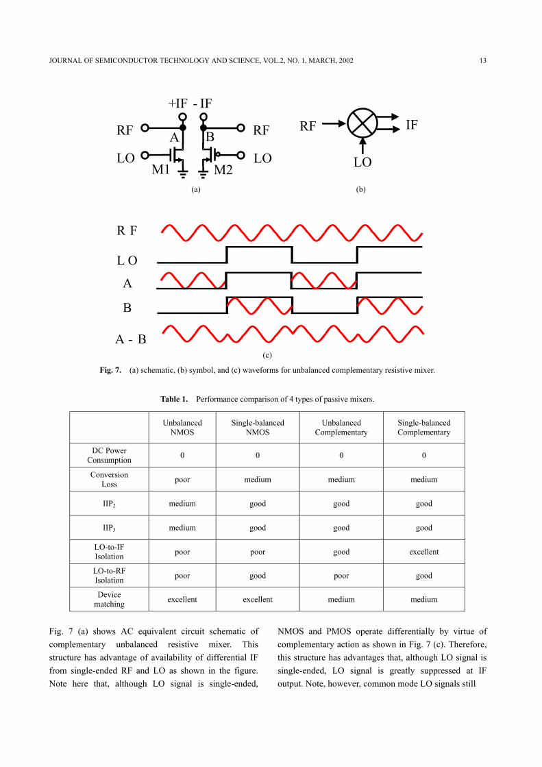
Fig. 7. (a) schematic, (b) symbol, and (c) waveforms for unbalanced complementary resistive mixer.
Table 1. Performance comparison of 4 types of passive mixers.
Unbalanced NMOS
Single-balanced NMOS
Unbalanced Complementary
Single-balanced Complementary
DC Power Consumption 0 0 0 0
Conversion Loss poor medium medium medium
IIP2 medium good good good
IIP3 medium good good good
LO-to-IF Isolation poor poor good excellent
LO-to-RF Isolation poor good poor good
Device excellent excellent medium medium
matchingg. 7 (a) shows AC equivalent circuit schematic of mplementary unbalanced resistive mixer. This
ructure has advantage of availability of differential IF om single-ended RF and LO as shown in the figure. ote here that, although LO signal is single-ended,
NMOS and PMOS operate differentially by virtue of complementary action as shown in Fig. 7 (c). Therefore, this structure has advantages that, although LO signal is single-ended, LO signal is greatly suppressed at IF output. Note, however, common mode LO signals still
B. KIM et al. : SINGLE-ENDED DIFFERENTIAL RF CIRCUIT TOPOLOGIES UTILIZING COMPLEMENTARY MOS DEVICES 14
RF
+ LO
+ IF
RF
+ LO
- IF
A B RF
- LO
- IF
RF
- LO
+ IF
C D
M1 M2 M3 M4
(a)
RF
LO
IF
(b)
RF
LO
A
D
A+D
B+C
(A+D)- (B+C)
(c)
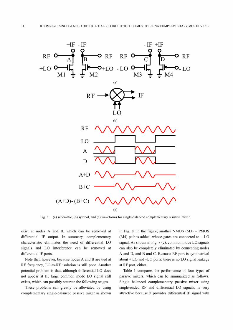
Fig. 8. (a) schematic, (b) symbol, and (c) waveforms for single-balanced complementary resistive mixer.
exist at nodes A and B, which can be removed at differential IF output. In summary, complementary characteristic eliminates the need of differential LO signals and LO interference can be removed at differential IF ports.
Note that, however, because nodes A and B are tied at RF frequency, LO-to-RF isolation is still poor. Another potential problem is that, although differential LO does not appear at IF, large common mode LO signal still exists, which can possibly saturate the following stages.
These problems can greatly be alleviated by using complementary single-balanced passive mixer as shown
in Fig. 8. In the figure, another NMOS (M3) – PMOS (M4) pair is added, whose gates are connected to – LO signal. As shown in Fig. 8 (c), common mode LO signals can also be completely eliminated by connecting nodes A and D, and B and C. Because RF port is symmetrical about + LO and –LO ports, there is no LO signal leakage at RF port, either.
Table 1 compares the performance of four types of passive mixers, which can be summarized as follows. Single balanced complementary passive mixer using single-ended RF and differential LO signals, is very attractive because it provides differential IF signal with
JOURNAL OF SEMICONDUCTOR TECHNOLOGY AND SCIENCE, VOL.2, NO. 1, MARCH, 2002
15
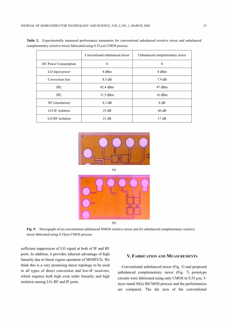
Table 2. Experimentally measured performance summaries for conventional unbalanced resistive mixer and unbalanced complementary resistive mixer fabricated using 0.35 µm CMOS process.
Conventional unbalanced mixer Unbalanced complementary mixer
DC Power Consumption 0 0
LO input power 4 dBm 4 dBm
Conversion loss 8.5 dB 7.9 dB
IIP2 42.4 dBm 47 dBm
IIP3 11.5 dBm 16 dBm
NF (simulation) 8.3 dB 8 dB
LO-IF isolation 25 dB 40 dB
LO-RF isolation 21 dB 17 dB
Fig. 1
(a)
(b)
Fig. 9. Micrograph of (a) conventional unbalanced NMOS resistive mixer and (b) unbalanced complementary resistive mixer fabricated using 0.35µm CMOS process.
sufficient suppression of LO signal at both of IF and RF ports. In addition, it provides inherent advantage of high linearity due to linear region operation of MOSFETs. We think this is a very promising mixer topology to be used in all types of direct conversion and low-IF receivers, which requires both high even order linearity and high isolation among LO, RF and IF ports.
V. FABRICATION AND MEASUREMENTS
Conventional unbalanced mixer (Fig. 5) and proposed unbalanced complementary mixer (Fig. 7) prototype circuits were fabricated using only CMOS in 0.35 µm, 3-layer metal SiGe BiCMOS process and the performances are compared. The die area of the conventional
B. KIM et al. : SINGLE-ENDED DIFFERENTIAL RF CIRCUIT TOPOLOGIES UTILIZING COMPLEMENTARY MOS DEVICES 16
unbalanced mixer and proposed mixer is 0.47 mm × 0.207 mm and 0.677 mm × 0.423 mm, respectively. To obtain symmetrical characteristics, the size of NMOS and PMOS is chosen as 100 µm/0.35 µm(W/L) and 350 µm/0.35 µm(W/L), respectively. The chip micrographs are shown in Fig. 9.
-20 -15 -10 -5 0 5 10
-20
-15
-10
-5
0
Con
vers
ion
Gai
n (d
LO Power (dBm )
Sim ulation M easurem ent
(a)
-2 0 -1 5 -1 0 -5 0 5 10
-2 0
-1 5
-1 0
-5
0
Co
nve
rsio
n G
ain
(d
L O P o w er (d B m )
S im u la tio n M e a su rem e n t
(b)
Fig. 10. Measured conversion gain vs. LO power for (a) conventional unbalanced NMOS resistive mixer and (b) unbalanced complementary resistive mixer.
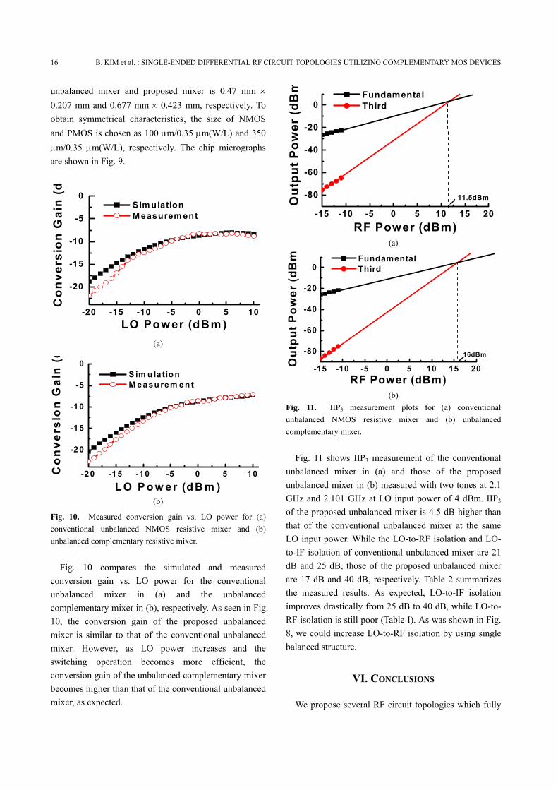
Fig. 10 compares the simulated and measured conversion gain vs. LO power for the conventional unbalanced mixer in (a) and the unbalanced complementary mixer in (b), respectively. As seen in Fig. 10, the conversion gain of the proposed unbalanced mixer is similar to that of the conventional unbalanced mixer. However, as LO power increases and the switching operation becomes more efficient, the conversion gain of the unbalanced complementary mixer becomes higher than that of the conventional unbalanced mixer, as expected.
-15 -10 -5 0 5 10 15 20
-80
-60
-40
-20
0
11.5dBmOut
put P
ower
(dB
m
RF Power (dBm)
Fundamental Third
(a)
-15 -10 -5 0 5 10 15 20
-80
-60
-40
-20
0
16dBm
Out
put P
ower
(dB
m
RF Power (dBm)
Fundamental Third
(b)
Fig. 11. IIP3 measurement plots for (a) conventional unbalanced NMOS resistive mixer and (b) unbalanced complementary mixer.
Fig. 11 shows IIP3 measurement of the conventional
unbalanced mixer in (a) and those of the proposed unbalanced mixer in (b) measured with two tones at 2.1 GHz and 2.101 GHz at LO input power of 4 dBm. IIP3 of the proposed unbalanced mixer is 4.5 dB higher than that of the conventional unbalanced mixer at the same LO input power. While the LO-to-RF isolation and LO-to-IF isolation of conventional unbalanced mixer are 21 dB and 25 dB, those of the proposed unbalanced mixer are 17 dB and 40 dB, respectively. Table 2 summarizes the measured results. As expected, LO-to-IF isolation improves drastically from 25 dB to 40 dB, while LO-to-RF isolation is still poor (Table I). As was shown in Fig. 8, we could increase LO-to-RF isolation by using single balanced structure.
VI. CONCLUSIONS
We propose several RF circuit topologies which fully
JOURNAL OF SEMICONDUCTOR TECHNOLOGY AND SCIENCE, VOL.2, NO. 1, MARCH, 2002
17
utilize complementary characteristics of NMOS and PMOS. Firstly, we introduce CCPP amplifier which has single-ended input/output and differential amplifying characteristics, leading to more than 30 dB improvement on IIP2. In addition, complementary resistive mixer is also proposed, which not only provides differential IF from single-ended RF, but much better linearity as well as isolation characteristics. Experimental results using 0.35 µm CMOS process show that the proposed mixer has 15 dB better LO-to-IF isolation, 4.6 dB better IIP2, and 4.5 dB better IIP3 characteristics, compared with conventional NMOS mixer. This proposed circuit topologies are expected to be a viable choice for integration of RF circuit in a single chip.
ACKNOWLEDGEMENT
The work at KAIST is supported by MICROS Research Center.
REFERENCES
[1] D. Gloria, A. Perrotin, R. Gonella and G. Morin, “BiCMOS MOSFET high frequency features for radiofrequency (RF) applications. Hot carrier effects on dynamic and noise parameters, impact on RF design features,” IEEE MTT-S Dig., pp. 831 – 834, 1999.
[2] R. H. Yan, K.F. Lee, D.Y. Jeon, Y.O. Kim, B.G. Park, M.R. Pinto, C.S. Rafferty, D.M. Tennant, E.H. Westerwick, G.M. Chin, M.D. Morris, K. Early, P. Mulgrew, W.M. Mansfield, R.K. Watts, A.M. Voshchenkov, J. Bokor, R.G. Swartz and A. Ourmazd, “High performance 0.1-µm room temperature Si MOSFETs,” IEEE Symposium on VLSI Technology Dig., pp. 86-87, 1992.
[3] J. Chen, S. Parke, J. King, F. Assaderaghi, P.K. Ko and C. Hu, “A high speed SOI technology with 12 ps/18 ps gate delay operating at 5 V/1.5 V,” Proc. International Electron Devices Meeting, pp. 35-38, 1992.
[4] B. Razavi, “A 5.2-GHz CMOS receiver with 62-dB image rejection,” IEEE Journal of Solid-State Circuits, vol. 36, no. 5, pp. 810-815, May 2001 .
[5] H. Samavati, H.R. Rategh, H.R. and T.H. Lee, “A fully-integrated 5 GHz CMOS wireless-LAN receiver,” Proc. IEEE International Solid-State Circuits Conference, pp. 208-209, 2001.
[6] P. Leroux, and M. Steyaert, “High-performance 5.2 GHz LNA with on-chip inductor to provide ESD protection,” Electronics Letters, vol. 37, no. 7, pp. 467-469, March
2001. [7] A.N.L. Chan, K.W.H. Ng, J.M.C. Wong, J.M.C. and H.C.
Luong, “A 1-V 2.4-GHz CMOS RF receiver front-end for bluetooth application,” Proc. IEEE International Symposium on Circuits and Systems, pp. 454-457, May 2001.
[8] Silicon Laboratories, Si4200 Data sheet, 2001. [9] Z. Zhang, L. Tsui, Z. Chen and J. Lau, “A CMOS self-
mixing-free front-end for direct conversion applications,” Proc. IEEE International Symposium on Circuits and Systems, pp. 386-389, May 2001.
[10] J. Jussila, J. Ryynanen, K. Kivakas, L. Sumanen, A. Parssinen and K. Haionen, “A 22 mA 3.7 dB NF direct conversion receiver for 3G WCDMA,” Proc. IEEE International Solid-State Circuits Conference, pp. 284-285, 2001.
[11] S. Tadjpour, E. Cijvat, E. Hegazi and A.A. Abidi, “A 900 MHz dual conversion low-IF GSM receiver in 0.35 µm CMOS,” Proc. IEEE International Solid-State Circuits Conference, pp. 292-293, 2001.
[12] F. Behbahani, Y. Kishigami, J. Leete and A.A. Abidi, “CMOS mixers and polyphase filters for large image rejection,” IEEE Journal of Solid-State Circuits, vol. 36, no. 6 , pp. 873-887, June 2001.
[13] Young Jin Kim, Hyung Chul Park, Il Ku Nam and Kwyro Lee, “Architecture and algorithm for ultra-high precision image rejection mixer using digital compensation,” IEE Electronics Letters, vol. 36, no. 19, pp 1064-1066, 2000
[14] B. Razavi, “RF Microelectronics,” Prentice Hall, 1998. [15] C.R.C. De Ranter and M.S.J. Steyaert, “A 0.25 µm
CMOS 17 GHz VCO,” Proc. IEEE International Solid-State Circuits Conference, pp. 370-371, 2001
[16] S. Park and W. Kim, “Design of a 1.8 GHz low-noise amplifier for RF front-end in a 0.8 µm CMOS technology,” IEEE Transactions on Consumer Electronics, vol. 47, no. 1, pp. 10-15, Feb. 2001.
[17] Z. Zhang, Z. Chen, L. Tsui and J. Lau, “A 930 MHz CMOS DC-offset-free direct-conversion 4-FSK receiver,” Proc. IEEE International Solid-State Circuits Conference, pp. 290-291, 2001.
[18] K. Lim, C.-H. Park, H.K. Ahn, J.J. Kim and B. Kim, “A fully integrated CMOS RF front-end with on-chip VCO for WCDMA applications,” Proc. IEEE International Solid-State Circuits Conference, pp. 286-287, 2001.
[19] M. Steyart, “Single chip CMOS RF transceivers: wishful thinking or reality,” IEE Seminar on Low Power IC Design (Ref. No. 2001/042), pp. 1/1 - 1/6, 2001
[20] S.-W. Lee, K.-Y. Lee, E. Song, Y.-J. Jung, H. Jeong, J.-M. Kim, H.-J. Lim, J.-W. Lee, J. Park, K. Lee, S.-l. Chae, D.-K. Jeong and W. Kim, “A single-chip 2.4 GHz direct-conversion CMOS transceiver with GFSK modem for bluetooth application,” Proc. IEEE Symposium on VLSI Circuits, pp. 245-246, 2001.
B. KIM et al. : SINGLE-ENDED DIFFERENTIAL RF CIRCUIT TOPOLOGIES UTILIZING COMPLEMENTARY MOS DEVICES 18
[21] J.J. Kucera, “Wideband BiCMOS VCO for GSM/UMTS direct conversion receivers,” Proc. IEEE International Solid-State Circuits Conference, pp. 374-375, 2001.
[22] A.M. ElSayed and M.I. Elmary, “Low-phase-noise LC quadrature VCO using coupled tank resonators in a ring structure,” IEEE Journal of Solid-State Circuits, vol. 36, no. 4 , pp. 701-705, April 2001.
[23] D. Ham and A. Hajimiri, “Design and optimization of a low noise 2.4 GHz CMOS VCO with integrated LC tank and MOSCAP tuning,” Proc. 2000 IEEE International Symposium on Circuits and Systems, pp. 331-334, 2000.
[24] D. Ham and A. Hajimiri, “Concepts and methods in optimization of integrated LC VCOs,” IEEE Journal of Solid-State Circuits, vol. 36, no. 6, pp. 896-909, June 2001.
[25] T.H. Lee, A. Hajimiri, “Oscillator phase noise: a tutorial,” IEEE Journal of Solid-State Circuits, vol. 35, no. 3 , pp. 326-336, March 2000 .
[26] T.C. Kuo, and B. Lusignan, “A 1.5 W class-F RF power amplifier in 0.2 µm CMOS technology,” Proc. IEEE International Solid-State Circuits Conference, pp. 154-155, 2001.
[27] R. Gupta, B.M. Ballweber, and D.J. Allstot, “Design and optimization of CMOS RF power amplifiers,” IEEE Journal of Solid-State Circuits, vol. 36, no. 2, pp. 166-175, Feb. 2001.
[28] R. Gupta and D.J. Allstot, “Parasitic-aware design and optimization of CMOS RF integrated circuits,” Proc. Radio Frequency Integrated Circuits (RFIC) Symposium, pp. 325-328, 1998.
[29] Bonkee Kim, Jin-Su Ko and Kwyro Lee, “Highly linear CMOS RF MMIC amplifier using multiple gated transistors and its Volterra series analysis,” Proc. MTT-S IEEE International Microwave Symposium, pp.515-518, 2001.
[30] S. Tanaka, F. Behbahani and A.A. Abidi, “A Linearization Technique For CMOS RF Power Amplifiers,” Proc. Symposium on VLSI Circuits, pp. 93-94, 1997.
[31] Bonkee Kim, Jin-Su Ko, and Kwyro Lee, “A New Linearization Technique for MOSFET RF Amplifier Using Multiple Gated Transistors,” IEEE Microwave and Guided Wave Letters, vol. 10, no. 9, pp. 371-374, 2000.
[32] Kwy-Ro Lee and Bon-Kee Kim, “PARALLEL PUSH-PULL AMPLIFIER USING COMPLEMENTARY DEVICE”, US Patent 6087900, 11 July 2000.
[33] Bonkee Kim, “Highly Linear CMOS RF Amplifier using gm Nonlinearity Cancellation and its Volterra Series Analysis,” Ph.D thesis, Korea Advanced Institute of Science and Technology, 2001.
[34] Kwyro Lee, Bonkee Kim and Ilku Nam, “Single-ended differential circuit using complementary devices”, Korea Patent filed, 2001.
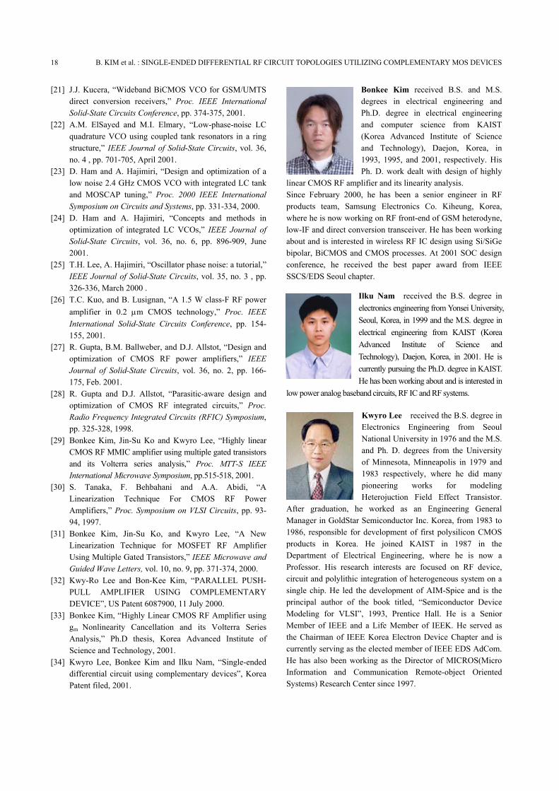
Bonkee Kim received B.S. and M.S. degrees in electrical engineering and Ph.D. degree in electrical engineering and computer science from KAIST (Korea Advanced Institute of Science and Technology), Daejon, Korea, in 1993, 1995, and 2001, respectively. His Ph. D. work dealt with design of highly
linear CMOS RF amplifier and its linearity analysis. Since February 2000, he has been a senior engineer in RF products team, Samsung Electronics Co. Kiheung, Korea, where he is now working on RF front-end of GSM heterodyne, low-IF and direct conversion transceiver. He has been working about and is interested in wireless RF IC design using Si/SiGe bipolar, BiCMOS and CMOS processes. At 2001 SOC design conference, he received the best paper award from IEEE SSCS/EDS Seoul chapter.
Ilku Nam received the B.S. degree in electronics engineering from Yonsei University, Seoul, Korea, in 1999 and the M.S. degree in electrical engineering from KAIST (Korea Advanced Institute of Science and Technology), Daejon, Korea, in 2001. He is currently pursuing the Ph.D. degree in KAIST. He has been working about and is interested in
low power analog baseband circuits, RF IC and RF systems.
Kwyro Lee received the B.S. degree in Electronics Engineering from Seoul National University in 1976 and the M.S. and Ph. D. degrees from the University of Minnesota, Minneapolis in 1979 and 1983 respectively, where he did many pioneering works for modeling Heterojuction Field Effect Transistor.
After graduation, he worked as an Engineering General Manager in GoldStar Semiconductor Inc. Korea, from 1983 to 1986, responsible for development of first polysilicon CMOS products in Korea. He joined KAIST in 1987 in the Department of Electrical Engineering, where he is now a Professor. His research interests are focused on RF device, circuit and polylithic integration of heterogeneous system on a single chip. He led the development of AIM-Spice and is the principal author of the book titled, “Semiconductor Device Modeling for VLSI”, 1993, Prentice Hall. He is a Senior Member of IEEE and a Life Member of IEEK. He served as the Chairman of IEEE Korea Electron Device Chapter and is currently serving as the elected member of IEEE EDS AdCom. He has also been working as the Director of MICROS(Micro Information and Communication Remote-object Oriented Systems) Research Center since 1997.