White Backlight LED Driver For Medium to Large LCD...
30
〇Product structure : Silicon monolithic integrated circuit 〇This product has no designed protection against radioactive rays . 1/27 TSZ02201-0T3T0C600030-1-2 © 2014 ROHM Co., Ltd. All rights reserved. 28.Aug.2014 Rev.001 TSZ22111 • 14 • 001 www.rohm.com White Backlight LED Driver For Medium to Large LCD Panels (Switching Regulator Type) BD8119FM-M General Description BD8119FM-M is a white LED driver with the capability to withstand high input voltage (36V Max). This driver has 4ch constant-current drivers integrated in 1-chip. Each channel can draw up to 150mA max for driving high brightness on LED. A current-mode buck-boost DC/DC controller is also integrated to achieve stable operation against unstable car-battery voltage input. This also removes the constraint of the number of LEDs in series connection. The brightness can be controlled by either PWM or VDAC techniques. Features ■ Integrated buck-boost current-mode DC/DC controller ■ Four integrated LED current driver channels (150mA Max each channel) ■ PWM Light Modulation (Minimum Pulse Width 25μs) ■ Built-in protection functions (UVLO, OVP, TSD, OCP, SCP) ■ Abnormal status detection function (OPEN/ SHORT) Applications Backlight for car navigation, dashboard panels, etc. Key Specifications Input Supply Voltage Range: 5.0V to 30V Standby Current: 4μA (Typ) LED Maximum Output Current: 150mA(Max) Operating Temperature Range: -40°C to +95°C Package W(Typ) x D(Typ) x H(Max) HSOP-M28 18.50mm x 9.90mm x 2.41mm Datasheet
Transcript of White Backlight LED Driver For Medium to Large LCD...

〇Product structure : Silicon monolithic integrated circuit 〇This product has no designed protection against radioactive rays
.
1/27
TSZ02201-0T3T0C600030-1-2 © 2014 ROHM Co., Ltd. All rights reserved. 28.Aug.2014 Rev.001 TSZ22111 • 14 • 001
www.rohm.com
White Backlight LED Driver For Medium to Large LCD Panels (Switching Regulator Type) BD8119FM-M General Description
BD8119FM-M is a white LED driver with the capability to withstand high input voltage (36V Max). This driver has 4ch constant-current drivers integrated in 1-chip. Each channel can draw up to 150mA max for driving high brightness on LED. A current-mode buck-boost DC/DC controller is also integrated to achieve stable operation against unstable car-battery voltage input. This also removes the constraint of the number of LEDs in series connection. The brightness can be controlled by either PWM or VDAC techniques.
Features
■ Integrated buck-boost current-mode DC/DC controller
■ Four integrated LED current driver channels
(150mA Max each channel)
■ PWM Light Modulation (Minimum Pulse Width 25µs)
■ Built-in protection functions (UVLO, OVP, TSD, OCP, SCP)
■ Abnormal status detection function (OPEN/ SHORT)
Applications
Backlight for car navigation, dashboard panels, etc.
Key Specifications Input Supply Voltage Range: 5.0V to 30V Standby Current: 4µA (Typ) LED Maximum Output Current: 150mA(Max) Operating Temperature Range: -40°C to +95°C
Package W(Typ) x D(Typ) x H(Max)
HSOP-M28 18.50mm x 9.90mm x 2.41mm
Datasheet

BD8119FM-M
2/27
TSZ02201-0T3T0C600030-1-2 © 2014 ROHM Co., Ltd. All rights reserved. www.rohm.com
TSZ22111・15・001 28.Aug.2014 Rev.001
Pin Configuration
Pin Descriptions
Pin Symbol Function Pin Symbol Function
1 COMP Error amplifier output 15 LED3 LED output 3
2 SS Soft start time-setting capacitance input 16 LED4 LED output 4
3 VCC Input power supply 17 OVP Over-voltage detection input
4 EN Enable input 18 VDAC DC variable light modulation input
5 RT Oscillation frequency-setting resistance input 19 ISET LED output current-setting resistance input
6 SYNC External synchronization signal input 20 PGND LED output GND
7 GND Small-signal GND 21 - No Connection
8 PWM PWM light modulation input 22 OUTL Low-side external MOSFET Gate Drive output
9 FAIL1 Failure signal output 23 DGND Low-side internal MOSFET Source output
10 FAIL2 LED open/short detection signal output 24 SW High-side external MOSFET Source pin
11 LEDEN1 LED output enable pin 1 25 OUTH High-side external MOSFET Gate Drive outpin
12 LEDEN2 LED output enable pin 2 26 CS DC/DC Current Sense Pin
13 LED1 LED output 1 27 BOOT High-side MOSFET Power Supply pin
14 LED2 LED output 2 28 VREG Internal reference voltage output
COMP 1
2
3
4
5
6
7
8
9
10
11
12
13
14
28
27
26
25
24
23
22
21
20
19
18
17
16
15
SS
VCC
EN
RT
SYNC
GND
PWM
FAIL1
FAIL2
LEDEN1
LEDEN2
LED2
LED1
VREG
BOOT
CS
OUTH
SW
DGND
OUTL
N.C.
PGND
ISET
VDAC
OVP
LED3
LED4
(TOP VIEW)

BD8119FM-M
3/27
TSZ02201-0T3T0C600030-1-2 © 2014 ROHM Co., Ltd. All rights reserved. www.rohm.com
TSZ22111・15・001 28.Aug.2014 Rev.001
Block Diagram
DGND
COMP
ERR AMP
VREG
+
-
VCC
EN
RT
OVP
OSC
Control Logic
UVLO TSD
-
-
+
SS
PWM
LED1
LED2
LED3 Current driver
ISET
PGND
PWM
CS
FAIL1
-
VREG
VDAC
GND
ISET
LED4
-
BOOT
OUTH
SW
+
-
FAIL2
LEDEN1 LEDEN2
SYNC
VREG
OVP
Timer Latch PWM
OCP
DRV
CTL
SLOPE
OCP OVP
Open Short Detect
Timer Latch Short Det
Open Det
OUTL

BD8119FM-M
4/27
TSZ02201-0T3T0C600030-1-2 © 2014 ROHM Co., Ltd. All rights reserved. www.rohm.com
TSZ22111・15・001 28.Aug.2014 Rev.001
Absolute Maximum Ratings (Ta=25°C)
Parameter Symbol Rating Unit
Power Supply Voltage VCC 36 V
BOOT ,OUTH Voltage VBOOT, VOUTH 41 V
SW,CS Voltage VSW, VCS, VOUTH 36 V
BOOT-SW Voltage VBOOT-SW 7 V
LED Output Voltage VLED1, VLED2, VLED3, VLED4 36 V
VREG, OVP, OUTL, FAIL1, FAIL2, LEDEN1, LEDEN2, ISET, VDAC, PWM, SS, COMP, RT, SYNC, EN Voltage
VREG, VOVP, VOUTL, VFAIL1, VFAIL2,
VLEDEN1, VLEDEN2, VISET, VVDAC,
VPWM, VSS, VCOMP, VRT, VSYNC, VEN -0.3 to +7 < VCC V
Power Consumption Pd 2.20 (Note 1)
W
Operating Temperature Range Topr -40 to +95 °C
Storage Temperature Range Tstg -55 to +150 °C
LED Maximum Output Current ILED 150 (Note 2) (Note 3)
mA
(Note 1) IC mounted on glass epoxy board measuring 70mm x 70mm x 1.6mm, power dissipated at a rate of 17.6mw/°C at temperatures above 25°C.
(Note 2) Dispersion figures for LED maximum output current and VF are correlated. Please refer to data on separate sheet. (Note 3) Amount of current per channel. Caution: Use of the IC in excess of absolute maximum ratings (such as the input voltage or operating temperature range) may result in damage to the IC. Assumptions should not be made regarding the state of the IC (e.g., short mode or open mode) when such damage is suffered. If operational values are expected to exceed the maximum ratings for the device, consider adding protective circuitry (such as fuses) to eliminate the risk of damaging the IC.
Recommended Operating Conditions (Ta=25°C)
Parameter Symbol Rating Unit
Power Supply Voltage VCC 5.0 to 30 V
Oscillating Frequency Range fOSC 250 to 550 kHz
External Synchronization Frequency Range (Note 4) (Note 5) fSYNC fOSC to 550 kHz
External Synchronization Pulse Duty Range fSDUTY 40 to 60 %
(Note 4) Connect SYNC to GND or OPEN when not using external frequency synchronization. (Note 5) Do not switch between internal and external synchronization when an external synchronization signal is inputted to the device.

BD8119FM-M
5/27
TSZ02201-0T3T0C600030-1-2 © 2014 ROHM Co., Ltd. All rights reserved. www.rohm.com
TSZ22111・15・001 28.Aug.2014 Rev.001
Electrical Characteristics (unless otherwise specified, VCC=12V Ta=25°C)
Parameter Symbol Limit
Unit Conditions Min Typ Max
Circuit Current ICC - 7 14 mA EN=Hi, SYNC=Hi, RT=OPEN PWM=Low, ISET=OPEN, CIN=10µF
Standby Current IST - 4 8 µA EN=Low
[VREG Block (VREG)]
Reference Voltage VREG 4.5 5 5.5 V IREG=-5mA, CREG=2.2µF
[OUTH Block]
OUTH High-side ON-Resistance RONHH 1.0 3 4.5 Ω ION=-10mA
OUTH Low-side ON-Resistance RONHL 0.5 2 3.0 Ω ION=10mA
Over-Current Protection Operating Voltage
VOLIMIT VCC
-0.66 VCC -0.6
VCC -0.54
V
[OUTL Block]
OUTL High-side ON-Resistance RONLH 1.0 3 4.5 Ω ION=-10mA
OUTL Low-side ON-Resistance RONLL 0.5 2 3.0 Ω ION=10mA
[SW Block]
SW Low-side ON-Resistance RON_SW 1.0 2.0 4.0 Ω ION_SW=10mA
[Error Amplifier Block]
LED Voltage VLED 0.9 1.0 1.1 V
COMP Sink Current ICOMPSINK 15 25 35 µA VLED=2V, VCOMP=1V
COMP Source Current ICOMPSOURCE -35 -25 -15 µA VLED=0V, VCOMP=1V
[Oscillator Block]
Oscillating Frequency fOSC 250 300 350 KHz RRT=100kΩ
[OVP Block]
Over-voltage Detection Reference Voltage
VOVP 1.9 2.0 2.1 V VOVP=Sweep up
OVP Hysteresis Width VOHYS 0.45 0.55 0.65 V VOVP=Sweep down
SCP Latch OFF Delay Time tSCP 70 100 130 ms RRT=100kΩ
[UVLO Block ]
UVLO Voltage VUVLO 4.0 4.3 4.6 V VCC : Sweep down
UVLO Hysteresis Width VUHYS 50 150 150 mV VCC : Sweep up

BD8119FM-M
6/27
TSZ02201-0T3T0C600030-1-2 © 2014 ROHM Co., Ltd. All rights reserved. www.rohm.com
TSZ22111・15・001 28.Aug.2014 Rev.001
Electrical Characteristics – continued (unless otherwise specified, VCC=12V Ta=25°C)
Parameter Symbol Limit
Unit Conditions Min Typ Max
[LED Output Block]
LED Current Relative Dispersion Width
ΔILED1 -3 - +3 % ILED=50mA, ΔILED1=(ILEDILED_AVG-1) x 100
LED Current Absolute Dispersion Width
ΔILED2 -5 - +5 % ILED=50mA, ΔILED2=(ILED50mA-1) x 100
ISET Voltage VISET 1.96 2.0 2.04 V RISET 1=120kΩ
PWM Minimum Pulse Width Tmin 25 - - µs fPWM=150Hz, ILED=50mA
PWM Maximum Duty Dmax - - 100 % fPWM=150Hz, ILED=50mA
PWM Frequency fPWM - - 20 KHz Duty=50%, ILED=50mA
VDAC Gain GVDAC - 25 - mA/V VDAC=0V to 2V, RISET=120kΩ ILED=VDAC ÷ RISET x Gain
Open Detection Voltage VOPEN 0.2 0.3 0.4 V VLED= Sweep down
LED Short Detection Voltage VSHORT 4.4 4.7 5.0 V VOVP= Sweep up
LED Short Latch OFF Delay Time tSHORT 70 100 130 ms RRT=100kΩ
PWM Latch OFF Delay Time tPWM 70 100 130 ms RRT=100kΩ
[Logic Inputs (EN, SYNC, PWM, LEDEN1, LEDEN2)]
Input HIGH Voltage VINH 2.1 - 5.5 V
Input LOW Voltage VINL GND - 0.8 V
Input Current 1 IIN 20 35 50 µA VIN=5V (SYNC, PWM, LEDEN1, LEDEN2)
Input Current 2 IEN 15 25 35 µA VEN=5V (EN)
[FAIL Output (Open Drain) ]
FAIL LOW Voltage VOL - 0.1 0.2 V IOL=0.1mA

BD8119FM-M
7/27
TSZ02201-0T3T0C600030-1-2 © 2014 ROHM Co., Ltd. All rights reserved. www.rohm.com
TSZ22111・15・001 28.Aug.2014 Rev.001
Typical Performance Curves (Unless otherwise specified, Ta=25°C)
[kH
z]
[V]
4.5
4.7
4.9
5.1
5.3
5.5
-40 -15 10 35 60 85TEMPERATURE:Ta [℃]
OU
TP
UT
VO
LT
AG
E:V
RE
G [V
]
VCC=12V
Figure 1. Output Voltage vs Temperature
Ou
tpu
t V
oltag
e :
VR
EG [
V]
Temperature : Ta [°C]
200
240
280
320
360
400
-40 -15 10 35 60 85TEMPERATURE:Ta [℃]
SW
ITC
HIN
G F
RE
QU
EN
CY
:FO
SC
[kH
z]
VCC=12V
Figure 2. Switching Frequency vs Temperature
Sw
itch
ing
Fre
que
ncy :
fO
SC
[kH
z]
Temperature : Ta [°C]
45
47
49
51
53
55
0.5 1.5 2.5 3.5 4.5
LED VOLTAGE:VLED[V]
OU
TP
UT
CU
RR
EN
T :IL
ED
[mA
]
VCC= 12V
Figure 3. Output Current vs LED Voltage (ILED Depend on VLED)
Ou
tpu
t C
urr
en
t : I L
ED [
mA
]
LED Voltage : VLED [V]
45
47
49
51
53
55
-40 -15 10 35 60 85
TEMPERATURE:Ta [℃]
OU
TP
UT
CU
RR
EN
T :IL
ED
[mA
]
VCC= 12V
Figure 4. Output Current vs Temperature
Ou
tpu
t C
urr
en
t : I L
ED [
mA
]
Temperature : Ta [°C]

BD8119FM-M
8/27
TSZ02201-0T3T0C600030-1-2 © 2014 ROHM Co., Ltd. All rights reserved. www.rohm.com
TSZ22111・15・001 28.Aug.2014 Rev.001
Typical Performance Curves – continued
(Unless otherwise specified, Ta=25°C)
0
10
20
30
40
50
0 0.5 1 1.5 2
VDAC VOLTAGE:VDAC[V]
OU
TP
UT
CU
RR
EN
T :IL
ED
[m
A]
Figure 5. Output Current vs VDAC Voltage
(VDAC Gain①)
Ou
tpu
t C
urr
en
t : I L
ED [
mA
]
VDAC Voltage : VDAC [V]
0
1
2
3
4
5
0 0.02 0.04 0.06 0.08 0.1
VDAC VOLTAGE:VDAC[V]
OU
TP
UT
CU
RR
EN
T :IL
ED
[m
A]
Figure 6. Output Current vs VDAC Voltage
(VDAC Gain②)
Ou
tpu
t C
urr
en
t : I L
ED [
mA
]
VDAC Voltage : VDAC [V]
25
40
55
70
85
100
25 150 275 400 525
OUTPUT CURRENT [mA]
EFF
ICIE
NC
Y [%
]
VCC=5V
VCC=30V VCC=12V
Figure 7. Efficiency vs Output Current (Depend on Input Voltage)
Effic
iency [
%]
Output Current [mA]
25
40
55
70
85
100
25 150 275 400 525
OUTPUT CURRENT [mA]
EFFICIENCY
[%
]
VCC=4V
VCC=15V VCC=30V
Figure 8. Efficiency vs Output Current (Depend on Output Voltage)
Effic
iency [
%]
Output Current [mA]
BD8119FM-M
9/27
TSZ02201-0T3T0C600030-1-2 © 2014 ROHM Co., Ltd. All rights reserved. www.rohm.com
TSZ22111・15・001 28.Aug.2014 Rev.001
Typical Performance Curves – continued
(Unless otherwise specified, Ta=25°C)
0
2
4
6
8
10
0 1 2 3 4 5EN VOLTAGE:VEN [V]
OUT
PU
T V
OLT
AG
E:V
REG
[V]
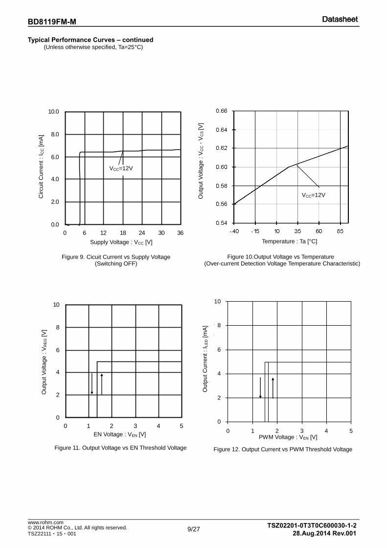
Figure 11. Output Voltage vs EN Threshold Voltage
Ou
tpu
t V
oltag
e :
VR
EG [
V]
EN Voltage : VEN [V]
VCC=12V
Figure 10.Output Voltage vs Temperature (Over-current Detection Voltage Temperature Characteristic)
Ou
tpu
t V
oltag
e :
VC
C -
VC
S [V
]
Temperature : Ta [°C]
0.0
2.0
4.0
6.0
8.0
10.0
0 6 12 18 24 30 36
SUPPLY VOLTAGE:Vcc [V]
OU
TP
UT
CA
RR
EN
T:Icc
[m
A]
VCC=12V
Figure 9. Cicuit Current vs Supply Voltage (Switching OFF)
Cir
cu
it C
urr
ent
: I C
C [m
A]
Supply Voltage : VCC [V]
0
2
4
6
8
10
0 1 2 3 4 5PWM VOLTAGE:VEN [V]
OU
TPU
TC
UR
REN
T :IL
ED
[m
A]
Figure 12. Output Current vs PWM Threshold Voltage
Ou
tpu
t C
urr
en
t : I L
ED [
mA
]
PWM Voltage : VEN [V]

BD8119FM-M
10/27
TSZ02201-0T3T0C600030-1-2 © 2014 ROHM Co., Ltd. All rights reserved. www.rohm.com
TSZ22111・15・001 28.Aug.2014 Rev.001
Application Information
1. 5V Voltage Reference (VREG) 5V (Typ) is generated from the VCC input voltage when the enable pin is set high. This voltage is used to power the internal circuitry as well as the voltage source for device pins that need to be fixed to a logical HIGH.
UVLO protection is integrated into the VREG pin. The voltage regulation circuitry operates uninterrupted for output voltages higher than 4.5V (Typ). If output voltage drops to 4.3V (Typ) or lower, UVLO operates and turns the IC OFF. Connect a capacitor (CREG = 2.2µF Typ) to the VREG terminal for phase compensation. Operation may become unstable if CREG is not connected.
2. Constant-current LED Drivers
If less than four constant-current drivers are used, unused channels should be switched OFF based on LEDEN pin configuration. The truth table for these pins is shown below. If a driver output is enabled but not used (i.e. left open), the IC’s open circuit-detection circuitry will operate. Please keep the unused pins open. The LEDEN terminals are pulled down internally in the IC, so if left open, the IC will recognize them as logic LO. However, they should be connected directly to VREG or fixed to a logic HI when in use.
LED EN
LED
〈1〉 〈2〉 1 2 3 4
L L ON ON ON ON
H L ON ON ON OFF
L H ON ON OFF OFF
H H ON OFF OFF OFF
(1) Output Current Setting
LED current is computed based on the following equation:
AGAINRVVVI SETISETDACLED /0.2min ,
(min[VDAC , 2.0V] = the smaller value of either VDAC or VISET; GAIN = set by internal circuitry.) In applications where an external signal is used for output current control, a control voltage in the range of 0.1V to 2.0V can be connected on the VDAC pin to control according to the above equation. If an external control signal is not used, connect the VDAC pin to VREG (do not leave the pin open as it may cause IC malfunction). Also, do not switch individual channels on or OFF using LEDEN pin while operating in PWM mode.
The following diagram illustrates the relation between ILED and GAIN.
In PWM intensity control mode, the ON/OFF state of each current driver is controlled directly by the input signal on the PWM pin; thus, the duty ratio of the input signal on the PWM pin equals the duty ratio of the LED current. When not controlling intensity at PWM, fix the PWM terminal to a high voltage (100%). Output light intensity is greatest at 100% input.
PWM
ILED(50mA/div)
PWM
ILED
PWM=150Hz Duty=50% PWM=150Hz Duty=0.38%
ILED vs GAIN
2950
3000
3050
3100
3150
3200
3250
3300
3350
0 20 40 60 80 100 120 140 160
ILED[mA]
GA
IN
ILED vs GAIN
ILED [mA]
GA
IN
ILED[mA] GAIN10 321520 308030 303040 299550 300060 302070 304080 307090 3105100 3140110 3175120 3210130 3245140 3280150 3330
ILED[mA]

BD8119FM-M
11/27
TSZ02201-0T3T0C600030-1-2 © 2014 ROHM Co., Ltd. All rights reserved. www.rohm.com
TSZ22111・15・001 28.Aug.2014 Rev.001
3. Buck-Boost DC/DC Controller
(1) Number of LEDs in Series Connection Output voltage of the DCDC converter is controlled such that the forward voltage over each of the LEDs on the output is set to 1.0V (Typ). DCDC operation is performed only when the LED output is operating. When two or more LED outputs are operating simultaneously, the LED voltage output is held at 1.0V (Typ) per LED from the set of LEDs in series with the highest VF value. The voltages of other LED outputs are increased only in relation to the fluctuation of voltage over these LEDs in series. Consideration should be given to the change in power dissipation due to variations in VF of the LEDs. Please determine the allowable maximum VF variance of the total LEDs in series by using the description as shown below:
VF variation allowable voltage 3.7V(Typ) = short detecting voltage 4.7V(Typ) - LED control voltage 1.0V(Typ) The number of LEDs that can be connected in series is limited due to the open-circuit protection circuit, which engages at 85% of the set OVP voltage. Therefore, the maximum output voltage of the under normal operation becomes seriesinLEDsofnumbermaximumN/V1.0V30.6where0.85,36V30.6V F .
(2) Over-voltage Protection Circuit (OVP)
The output of the DCDC converter should be connected to the OVP pin using a voltage divider. In determining an appropriate trigger voltage for OVP function, consider the total number of LEDs in series and the maximum variation in VF. Also, bear in mind that over-current protection (OCP) is triggered at 0.85 x OVP trigger voltage. If the OVP function operates, it will not release unless the DCDC voltage drops to 72.5% of the OVP trigger voltage. For example, if ROVP1 (output voltage side), ROVP2 (GND side), and DCDC voltage VOUT are conditions for OVP, then:
VRRRV OVPOVPOVPOUT 0.2/ 221
OVP will operate when VOUT > 32 V if ROVP1 = 330 kΩ and ROVP2 = 22 kΩ.
(3) Buck-boost DC/DC Converter Oscillation Frequency (fOSC)
The regulator’s internal triangular wave oscillation frequency can be set using a resistor connected to the RT pin (pin 26). This resistor determines the charge/discharge current to the internal capacitor, thereby changing the oscillating frequency. Refer to the following theoretical formula when setting RT:
kHzα
ΩR1030f
RT
6
OSC
30 x 10
6 (V/A/S) is a constant (±16.6%) determined by the internal circuitry, and α is a correction factor that varies in
relation to RT: {RT: α = 50kΩ: 0.98, 60kΩ: 0.985, 70kΩ: 0.99, 80kΩ: 0.994, 90kΩ: 0.996, 100kΩ: 1.0, 150kΩ: 1.01, 200kΩ: 1.02, 300kΩ: 1.03, 400kΩ: 1.04, 500kΩ: 1.045 }
A resistor in the range of 62.6kΩ to 523kΩ is recommended. Settings that deviate from the frequency range shown below may cause switching to stop, and proper operation cannot be guaranteed.
Figure 13. Switching Frequency vs RT
(4) External DC/DC Converter Oscillating Frequency Synchronization (fSYNC) Do not switch from external to internal oscillation of the DC/DC converter if an external synchronization signal is present on the SYNC pin. When the signal on the SYNC terminal is switched from high to low, a delay of about 30µs (Typ) occurs before the internal oscillation circuitry starts to operate (only the rising edge of the input clock signal on the SYNC terminal is recognized). Moreover, if external input frequency is less than the internal oscillation frequency, the internal oscillator will operate after the above-mentioned 30µs (Typ) delay; thus, do not input a synchronization signal with a frequency less than the internal oscillation frequency.
50K
150K
250K
350K
450K
550K
0 100 200 300 400 500 600 700 800
RT [kΩ ]
周波
数 [
kHz]
Fre
qu
ency [kH
z]
RT [kΩ]

BD8119FM-M
12/27
TSZ02201-0T3T0C600030-1-2 © 2014 ROHM Co., Ltd. All rights reserved. www.rohm.com
TSZ22111・15・001 28.Aug.2014 Rev.001
(5) Soft Start Function The soft-start (SS) limits the current and slows the rise-time of the output voltage during the start-up, hence it leads to prevention of the overshoot on the output voltage and the inrush current.
(6) Self-diagnostic Functions
The operating status of the built-in protection circuitry is propagated to FAIL1 and FAIL2 pins (open-drain outputs). FAIL1 becomes low when UVLO, TSD, OVP, or SCP protection is engaged, whereas FAIL2 becomes low when open or short LED is detected.
(7) Operation of the Protection Circuitry (a) Under-Voltage Lock Out (UVLO)
The UVLO shuts down all the circuits other than VREG when VCC 4.3V (Typ).
(b) Thermal Shut Down (TSD) The TSD shuts down all the circuits other than VREG when the Tj reaches 175°C (TYP), and releases when the Tj becomes below 150°C (Typ).
(c) Over-Current Protection (OCP) The OCP detects the current through the power-FET by monitoring the voltage of the high-side resistor, and activates when the CS voltage becomes less than VCC-0.6V (Typ). When the OCP is activated, the external capacitor of the SS pin becomes discharged and the switching operation of the DCDC turns OFF.
(d) Over Voltage Protection (OVP) The output voltage of the DCDC is detected with the OVP-pin voltage, and the protection activates when the OVP-pin voltage becomes greater than 2.0V (Typ). When the OVP is activated, the external capacitor of the SS pin becomes discharged and the switching operation of the DCDC turns OFF.
(8) Short Circuit Protection (SCP)
When the LED-pin voltage becomes less than 0.3V (Typ), the internal counter starts operating and latches OFF the circuit approximately after 100ms (when fOSC = 300kHz). If the LED-pin voltage becomes over 0.3V before 100ms, then the counter resets. When the LED anode (i.e. DCDC output voltage) is shorted to ground, then the LED current becomes OFF and the LED-pin voltage becomes low. Furthermore, the LED current also becomes OFF when the LED cathode is shorted to ground. Hence in summary, the SCP works with both cases of the LED anode and the cathode being shorted.
(9) LED Open Detection
When the LED-pin voltage 0.3V (Typ) as well as OVP-pin voltage 1.7V (Typ) simultaneously, the device detects as LED open and latches OFF that particular channel.
UVLO
TSD
OVP
OCP
S
R
Q SCP
EN=Low
UVLO/TSD
FAIL1
EN=Low
UVLO/TSD
FAIL2
MASK
Counter
OPEN
SHORT S
R
Q

BD8119FM-M
13/27
TSZ02201-0T3T0C600030-1-2 © 2014 ROHM Co., Ltd. All rights reserved. www.rohm.com
TSZ22111・15・001 28.Aug.2014 Rev.001
(10) LED Short Detection
When the LED-pin voltage 4.7V (Typ) and OVP-pin voltage 1.6V (Typ) simultaneously, the internal counter starts operating and the only detected channel (as LED short) latches OFF approximately after 100ms (when fOSC= 300kHz). With the PWM brightness control, the detecting operation is processed only when PWM-pin = High. If the condition of the detection operation is released before 100ms (when fOSC = 300kHz), then the internal counter resets. (Note) The counter frequency is the DCDC switching frequency determined by the RT. The latch proceeds at the count of 32770.
Protection Detecting Condition
Operation after detect [Detect] [Release]
UVLO VREG<4.3V VREG>4.5V All blocks shut down
TSD Tj>175°C Tj<150°C All blocks (except VREG) shut down
OVP VOVP>2.0V VOVP<1.45V SS discharges
OCP VCS≤VCC-0.6V VCS>VCC-0.6V SS discharges
SCP VLED<0.3V
(100ms delay when fOSC=300kHz)
EN or UVLO Counter starts and then latches OFF all blocks (except VREG)
LED open VLED<0.3V & VOVP>1.7V EN or UVLO Only the detected channel latches OFF
LED short VLED>4.7V & VOVP<1.6V
(100ms delay when fOSC=300kHz)
EN or UVLO Only the detected channel latches OFF (after the counter sets)

BD8119FM-M
14/27
TSZ02201-0T3T0C600030-1-2 © 2014 ROHM Co., Ltd. All rights reserved. www.rohm.com
TSZ22111・15・001 28.Aug.2014 Rev.001
4. Protection Sequence
(Note 1) Turn ON the EN after the VCC is ON (Note 2) SYNC and PWM inputs are allowed to be on before the VCC is ON (Note 3) Approximately 100ms of delay when fOSC = 300kHz (Note 4) This waveform is pulled up by a external supply.
① Case for LED2 in open-mode
When VLED2 < 0.3V and VOVP > 1.7V simultaneously, then LED2 becomes off and FAIL2 becomes low
② Case for LED3 in short-mode
When VLED3 > 4.7V and VOVP < 1.6V simultaneously, then LED3 becomes off after 100ms approx
③ Case for LED4 in short to GND
③-1 DCDC output voltage increases, and then SS dichages and FAIL1 becomes low
③-2 Detects VLED4<0.3V and shuts down after approximately 100ms
VCC
EN
UVLO
VDAC
SYNC
PWM
SS
ILED1
ILED2
ILED3
ILED4
VLED1
VLED2
VLED3
VLED4
VOVP
FAIL1
FAIL2
④
①
4.5V
②
1.0V
<0.3V
>4.7V
100ms *3
0.3V
100ms *3
2.0V
③
1.7V
*1
*2
*2
*1
*4
VREG
(Note 1)
(Note 2)
(Note 2)
(Note 3)
(Note 4)
(Note 1)
(Note 3)

BD8119FM-M
15/27
TSZ02201-0T3T0C600030-1-2 © 2014 ROHM Co., Ltd. All rights reserved. www.rohm.com
TSZ22111・15・001 28.Aug.2014 Rev.001
5. Procedure for External Components Selection Follow the steps as shown below for selecting the external components
(1) Work out IL_MAX from the operating conditions.
(2) Select the value of RCS such that IOCP > IL_MAX
(3) Select the value of L such that 0.05V/µs < VOUT / L < 0.3V/ µs
(4) Select coil, schottky diodes, MOSFET and RCS which meet with the ratings
(5) Select the output capacitor which meets with the ripple voltage requirements
(6) Select the input capacitor
(7) Work on the compensation circuit
(8) Work on the Over-Voltage Protection (OVP) setting
(9) Work on the soft-start setting
(10) Verify experimentally
Feedback the value of L

BD8119FM-M
16/27
TSZ02201-0T3T0C600030-1-2 © 2014 ROHM Co., Ltd. All rights reserved. www.rohm.com
TSZ22111・15・001 28.Aug.2014 Rev.001
(1) Computation of the Input Peak Current and IL_MAX ① Calculation of the maximum output voltage (VOUT_MAX)
To calculate the VOUT_MAX, it is necessary to take into account the VF variation and the number of LED connected in series.
VNVVV FFMAXOUT 0.1_ Where:
ΔVF is the VF Variation N is the Number of LED connection in series
② Calculation of the output current IOUT
MII LEDOUT 05.1 Where:
M is the Number of LED connections in parallel
③ Calculation of the input peak current IL_MAX
INOUTOUTNIAVGL
LAVGLMAXL
VIVVI
III
/
21
_
__
OUTIN
OUT
OSC
INL VV
VfL
VI
1
(a) The worst case scenario for VIN is when it is at the minimum, and thus the minimum value should be applied in the
equation. (b) An L value of 10µF to 47µF is recommended. The current-mode type of DC/DC conversion is adopted for
BD8119FM-M, which is optimized with the use of the recommended L value in the design stage. This recommendation is based upon the efficiency as well as the stability. L values outside this recommended range may cause irregular switching waveform and hence deterioration of stable operation.
(c) η (efficiency) is approximately 80%
External Application Circuit
(2) The Setting of Over-Current Protection Choose RCS with the use of the equation VOCP_MIN (=0.54V) / RCS > IL_MAX When investigating the margin, it is worth noting that the L value may vary by approximately ±30%.
VIN
RCS
D1
L D2
M2
M1
COUT
VOUT
IL
CS
Where: η is the efficiency fOSC is the switching frequency

BD8119FM-M
17/27
TSZ02201-0T3T0C600030-1-2 © 2014 ROHM Co., Ltd. All rights reserved. www.rohm.com
TSZ22111・15・001 28.Aug.2014 Rev.001
(3) The Selection of the L In order to achieve stable operation of the current-mode DC/DC converter, we recommend selecting the L value in the range indicated below:
sVLRVsV CSOUT /3.0]/[05.0
The smaller LRV CSOUT allows stability improvement but slows down the response time.
(4) Selection of coil L, diode D1 and D2, MOSFET M1 and M2, and RCS
Current rating Voltage Rating Heat Loss
Coil L > IL_MAX ―
Diode D1 > IOCP > VIN_MAX
Diode D2 > IOCP > VOUT
MOSFET M1 > IOCP > VIN_MAX
MOSFET M2 > IOCP > VOUT
RCS ― ― > IOCP2
x RCS
(Note 1) Allow some margin such as the tolerance of the external components when selecting. (Note 2) In order to achieve fast switching, choose a MOSFET with the smaller gate-capacitance.
(5) Selection of the Output Capacitor
Select the output capacitor COUT based on the requirement of the ripple voltage Vpp.
ESRLOSCINOUT
OUT
OUT
OUTpp RI
fVVV
CIV
⊿
1
Choose COUT that allows the Vpp to settle within the requirement. Allow some margin also, such as the tolerance of the external components.
(6) Selection of the Input Capacitor
A capacitor at the input is also required as the peak current flows between the input and the output in DC/DC conversion. An input capacitor greater than 10µF with the ESR smaller than 100mΩ is recommended. An input capacitor outside the recommended range may cause large ripple voltage at the input and may lead to malfunction.
BD8119FM-M
18/27
TSZ02201-0T3T0C600030-1-2 © 2014 ROHM Co., Ltd. All rights reserved. www.rohm.com
TSZ22111・15・001 28.Aug.2014 Rev.001
(7) Phase Compensation Guidelines In general, the negative feedback loop is stable when the following conditions are met:
Overall gain of 1 (0dB) with a phase lag of less than 150º (i.e., a phase margin of 30º or more)
However, as the DC/DC converter constantly samples the switching frequency, the gain-bandwidth (GBW) product of the entire series should be set to 1/10 the switching frequency of the system. Therefore, the overall stability characteristics of the application are as follows:
(a) Overall gain of 1 (0dB) with a phase lag of less than 150º (i.e., a phase margin of 30º or more) (b) GBW (frequency at gain 0dB) of 1/10 the switching frequency
Thus, to improve response within the GBW product limits, the switching frequency must be increased.
The key for achieving stability is to place fz near to the GBW. The GBW depends on a phase lag "fp1" that is decided by COUT and output impedance RL.
The phase-lead and the phase-lag are the following.
Phase-lead HzCpcRpc
fz2
1
Phase-lag HzRLC
fpOUT2
11
Good stability would be obtained when the fz is set between 1kHz to 10kHz.
In buck-boost applications, Right-Hand-Plane (RHP) Zero exists. This Zero has no gain but a pole characteristic in terms of phase. As this Zero may cause instability when it is in the control loop, it is necessary to bring this zero before the GBW.
HzLI
VVVVfLOAD
INOUTINOUTRHP
2/
Where: ILOAD is the Maximum Load Current
It is important to keep in mind that these are not very strict guidelines. Adjustments may have to be made to ensure stability in the actual circuitry. It is also important to note that stability characteristics can change greatly depending on factors such as substrate layout and load conditions. Therefore, when designing for mass-production, stability should be thoroughly investigated and confirmed in the actual physical design.
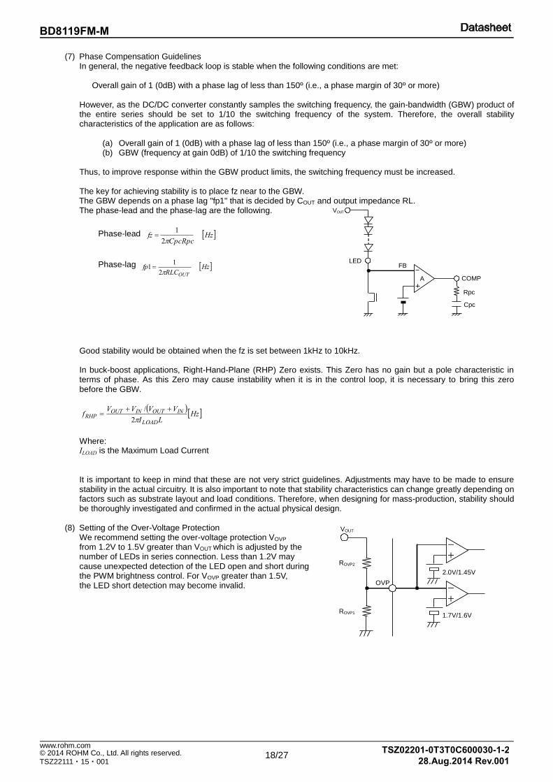
(8) Setting of the Over-Voltage Protection
We recommend setting the over-voltage protection VOVP from 1.2V to 1.5V greater than VOUT which is adjusted by the number of LEDs in series connection. Less than 1.2V may cause unexpected detection of the LED open and short during the PWM brightness control. For VOVP greater than 1.5V, the LED short detection may become invalid.
FB
A COMP
VOUT
Rpc
LED
Cpc
+
-
+
-
2.0V/1.45V
1.7V/1.6V
OVP
VOUT
ROVP2
ROVP1

BD8119FM-M
19/27
TSZ02201-0T3T0C600030-1-2 © 2014 ROHM Co., Ltd. All rights reserved. www.rohm.com
TSZ22111・15・001 28.Aug.2014 Rev.001
(9) Setting of the Soft-Start The soft-start allows minimizing the coil current as well as the overshoot of the output voltage at start-up.
For the capacitance, the range of 0.001µF to 0.1µF is recommended. Capacitance less than 0.001µF may cause overshoot on the output voltage. Capacitance greater than 0.1µF may cause massive reverse current through the parasitic elements of the IC that can damage the whole device. In case it is necessary to use the capacitance greater than 0.1µF, provide a reverse current protection diode at the VCC or a bypass diode placed between the SS-pin and the VCC.
Soft-start time tSS
s 0.7V/5µACt SSSS Where:
CSS is the capacitance at the SS-pin
(10) Verification of the Operation by Taking Measurements
The overall characteristic may change by load current, input voltage, output voltage, inductance, load capacitance, switching frequency, and the PCB layout. We strongly recommend verifying your design by taking the actual measurements.
Power Dissipation Power dissipation can be calculated as follows:
LEDFLEDCCSWREGissCCCC I1NΔVNVVfVC2VINPc
Where: ICC is the Maximum circuit current VCC is the Supply power voltage Ciss is the External FET capacitance VSW is the SW gate voltage fSW is the SE frequency VLED is the LED control voltage N is the LED parallel numeral ΔVF is the LED VF fluctuation ILED is the LED output current
Sample Calculation: 100mA3ΔV41.0V30V300kHz5V500pF30V10mA4Pc F
1622.5mW1.3W322.5mW4Pc3.0V,ΔVF
Figure 14
(Note 1) Power dissipation calculated when mounted on 70mm x 70mm x 1.6mm glass epoxy substrate (1-layer platform/copper thickness 18µm) (Note 2) Power dissipation changes with the copper foil density of the board. The area of the copper foil becomes the total area of the heat radiation fin and the foot pattern (connected directly with IC) of this IC. This value represents only observed values, not guaranteed values. Pd=2200mW ( 968mW): Substrate copper foil density 3% Pd=3200mW (1408mW): Substrate copper foil density 34% Pd=3500mW (1540mW): Substrate copper foil density 60% (Value within parentheses represents power dissipation when Ta=95°C) (Note 3) Please preserve that the ambient temperature + self-generation of heat becomes 150°C or less because this IC has a Tj=150°C. (Note 4) Please note the heat specification because there is a possibility that thermal resistance rises from the examination result of the temperature cycle by 20% or less.
Pd
[m
W]
0
500
1000
1500
2000
2500
0 0.5 1 1.5 2 2.5 3 3.5
LEDバラツキ⊿Vf[V]
ILED=
50mA
ILED=
100mA
ILED=
150mA
Power Dissipation
LED Fluctuation : ΔVF [V]
Ambient Temperature Ta[℃]
4
Pow
er
Dis
sipa
tion
Pd[
W]
2
1
0 150 125 100 75 50 25
3
(3) 3.50W
(2) 3.20W
(1) 2.20W
(1) θ ja=56.8℃/W (Substrate copper foil density 3%)
(2) θ ja=39.1℃/W (Substrate copper foil density34%) (3) θ ja=35.7℃/W (Substrate copper foil density60%)
95
Ambient Temperature : Ta [°C]
Po
wer
Dis
sip
atio
n :
Pd
[W
]
ILED= 50mA ILED=
100mA ILED= 150mA
Po
wer
Dis
sip
atio
n :
Pd
[W
]

BD8119FM-M
20/27
TSZ02201-0T3T0C600030-1-2 © 2014 ROHM Co., Ltd. All rights reserved. www.rohm.com
TSZ22111・15・001 28.Aug.2014 Rev.001
1. The coupling capacitors CVCC and CREG should be mounted as close as possible to the IC’s pins. 2. Large currents may pass through DGND and PGND, so each should have its own low-impedance
routing to the system ground. 3. Noise should be minimized as much as possible on pins VDAC, ISET, RT and COMP. 4. PWM, SYNC and LED1-4 carry switching signals, so ensure during layout that surrounding traces are
not affected by crosstalk.
1. COMP
2. SS
3. VCC
4. EN
5. RT
6. SYNC
7. GND
FIN. FIN
8. PWM
9. FAIL1
10. FAIL2
11. LEDEN1
12. LEDEN2
13. LED1
14. LED2
28. VREG
27. BOOT
26. CS
25. OUTH
24. SW
23. DGND
22. OUTL
FIN. FIN
21. FBR
20. PGND
19. ISET
18. VDAC
17. OVP
16. LED4
15. LED3
VCC VCC
CIN1 CIN2
CPC2
CPC1 RPC1
CSS
EN SW1
CRT RRT
SYNC
CIN3
PWM
RFL1 RFL2
VREG
FAIL1
FAIL2
VREG SW2
SW3
LED1
LED2
LED4
LED3
VDAC
RDAC VREG
CISET
RISET
D1
L1
D
G
M2 S COUT1 COUT2
D2
ROVP1
ROVP2
CBT
CREG
M1 S
D
G
RCS5
VREG
OUT
CCS RCS1 RCS2 RCS3

BD8119FM-M
21/27
TSZ02201-0T3T0C600030-1-2 © 2014 ROHM Co., Ltd. All rights reserved. www.rohm.com
TSZ22111・15・001 28.Aug.2014 Rev.001
Application Board Part List Serial No. Component Name Component Value Product Name Manufacturer
1 CIN1 10µF GRM31CB31E106KA75B Murata
2 CIN2 -
3 CIN3 -
4 CPC1 0.1µF
5 CPC2 - Murata
6 RPC1 510Ω
7 CSS 0.1µF GRM188B31H104KA92 Murata
8 RRT 100kΩ MCR03 Series Rohm
9 CRT -
10 RFL1 100kΩ MCR03 Series Rohm
11 RFL2 100kΩ MCR03 Series Rohm
12 CCS -
13 RCS1 620mΩ MCR100JZHFLR620 Rohm
14 RCS2 620mΩ MCR100JZHFLR620 Rohm
15 RCS3 -
16 RCS5 0Ω
17 CREG 2.2µF GRM188B31A225KE33 Murata
18 CBT 0.1µF GRM188B31H104KA92 Murata
19 M1 - RSS070N05 Rohm
20 M2 - RSS070N05 Rohm
21 D1 - RB050L-40 Rohm
22 D2 - RF201L2S Rohm
23 L1 33µH CDRH105R330 Sumida
24 COUT1 10µF GRM31CB31E106KA75B Murata
25 COUT2 10µF GRM31CB31E106KA75B Murata
26 ROVP1 30kΩ MCR03 Series Rohm
27 ROVP2 360kΩ MCR03 Series Rohm
28 RISET 120kΩ MCR03 Series Rohm
29 CISET -
30 RDAC 0Ω
1. The above values are fixed numbers for confirmed operation with the following conditions: VCC = 12V, four parallel
channels of five series-connected LEDs, and ILED=50mA. 2. Optimal values of external components depend on the actual application; these values should only be used as
guidelines and should be adjusted to fit the operating conditions of the actual application.
When performing open/short tests of the external components, the open condition of D1 or D2 may cause permanent damage to the driver and/or the external components. In order to prevent this, we recommend having parallel connections for D1 and D2.

BD8119FM-M
22/27
TSZ02201-0T3T0C600030-1-2 © 2014 ROHM Co., Ltd. All rights reserved. www.rohm.com
TSZ22111・15・001 28.Aug.2014 Rev.001
I/O Equivalent Circuits (terminal name follows pin number)
1. COMP 2. SS 4. EN
5. RT 6. SYNC, 8. PWM 9. FAIL1, 10. FAIL2
11. LEDEN1, 12. LEDEN2 13. LED1, 14. LED2, 15. LED3, 16. LED4 17. OVP
18. VDAC 19. ISET 22. OUTL
24. SW 25. OUTH 26. CS
27. BOOT 28. VREG 21.
CS 5K
VCC
N.C.
N.C. = no connection (open)
1K SS
VCC
VREG
10K
3.3V
150K
SYNC
PWM
1K
FAIL1
FAIL2
500
VDAC
VCC VREG
500 ISET
VCC
12.5
VREG VREG
100K
OUTL
VREG
VREG
BOOT
SW
VREG
VCC
VREG
205K
100K
10K
3.3V
150K
LEDEN1
LEDEN2
10K
COMP
2K
2K
VREG VREG
EN
175k
135k
10k
VCC
SW
VCC BOOT
100K
OUTH
BOOT
SW SW SW
5K
OVP 10K
VCC
RT
VREG
167
VCC
2.5K
5K LED1 to LED4

BD8119FM-M
23/27
TSZ02201-0T3T0C600030-1-2 © 2014 ROHM Co., Ltd. All rights reserved. www.rohm.com
TSZ22111・15・001 28.Aug.2014 Rev.001
Operational Notes
1. Reverse Connection of Power Supply
Connecting the power supply in reverse polarity can damage the IC. Take precautions against reverse polarity when connecting the power supply, such as mounting an external diode between the power supply and the IC’s power supply pins.
2. Power Supply Lines
Design the PCB layout pattern to provide low impedance supply lines. Separate the ground and supply lines of the digital and analog blocks to prevent noise in the ground and supply lines of the digital block from affecting the analog block. Furthermore, connect a capacitor to ground at all power supply pins. Consider the effect of temperature and aging on the capacitance value when using electrolytic capacitors.
3. Ground Voltage
Ensure that no pins are at a voltage below that of the ground pin at any time, even during transient condition.
4. Ground Wiring Pattern When using both small-signal and large-current ground traces, the two ground traces should be routed separately but connected to a single ground at the reference point of the application board to avoid fluctuations in the small-signal ground caused by large currents. Also ensure that the ground traces of external components do not cause variations on the ground voltage. The ground lines must be as short and thick as possible to reduce line impedance.
5. Thermal Consideration
Should by any chance the power dissipation rating be exceeded the rise in temperature of the chip may result in
deterioration of the properties of the chip. The absolute maximum rating of the Pd stated in this specification is when
the IC is mounted on a 70mm x 70mm x 1.6mm glass epoxy board. In case of exceeding this absolute maximum
rating, increase the board size and copper area to prevent exceeding the Pd rating.
6. Recommended Operating Conditions
These conditions represent a range within which the expected characteristics of the IC can be approximately obtained. The electrical characteristics are guaranteed under the conditions of each parameter.
7. Inrush Current
When power is first supplied to the IC, it is possible that the internal logic may be unstable and inrush current may flow instantaneously due to the internal powering sequence and delays, especially if the IC has more than one power supply. Therefore, give special consideration to power coupling capacitance, power wiring, width of ground wiring, and routing of connections.
8. Operation Under Strong Electromagnetic Field
Operating the IC in the presence of a strong electromagnetic field may cause the IC to malfunction.
9. Testing on Application Boards
When testing the IC on an application board, connecting a capacitor directly to a low-impedance output pin may subject the IC to stress. Always discharge capacitors completely after each process or step. The IC’s power supply should always be turned off completely before connecting or removing it from the test setup during the inspection process. To prevent damage from static discharge, ground the IC during assembly and use similar precautions during transport and storage.
10. Inter-pin Short and Mounting Errors Ensure that the direction and position are correct when mounting the IC on the PCB. Incorrect mounting may result in damaging the IC. Avoid nearby pins being shorted to each other especially to ground, power supply and output pin. Inter-pin shorts could be due to many reasons such as metal particles, water droplets (in very humid environment) and unintentional solder bridge deposited in between pins during assembly to name a few.

BD8119FM-M
24/27
TSZ02201-0T3T0C600030-1-2 © 2014 ROHM Co., Ltd. All rights reserved. www.rohm.com
TSZ22111・15・001 28.Aug.2014 Rev.001
Operational Notes – continued
11. Unused Input Pins
Input pins of an IC are often connected to the gate of a MOS transistor. The gate has extremely high impedance and extremely low capacitance. If left unconnected, the electric field from the outside can easily charge it. The small charge acquired in this way is enough to produce a significant effect on the conduction through the transistor and cause unexpected operation of the IC. So unless otherwise specified, unused input pins should be connected to the power supply or ground line.
12. Regarding the Input Pin of the IC
This monolithic IC contains P+ isolation and P substrate layers between adjacent elements in order to keep them isolated. P-N junctions are formed at the intersection of the P layers with the N layers of other elements, creating a parasitic diode or transistor. For example (refer to figure below):
When GND > Pin A and GND > Pin B, the P-N junction operates as a parasitic diode. When GND > Pin B, the P-N junction operates as a parasitic transistor.
Parasitic diodes inevitably occur in the structure of the IC. The operation of parasitic diodes can result in mutual interference among circuits, operational faults, or physical damage. Therefore, conditions that cause these diodes to operate, such as applying a voltage lower than the GND voltage to an input pin (and thus to the P substrate) should be avoided.
Figure 15. Example of monolithic IC structure
13. Area of Safe Operation (ASO) Operate the IC such that the output voltage, output current, and power dissipation are all within the Area of Safe Operation (ASO).
14. Thermal Shutdown Circuit(TSD)
This IC has a built-in thermal shutdown circuit that prevents heat damage to the IC. Normal operation should always be within the IC’s power dissipation rating. If however the rating is exceeded for a continued period, the junction temperature (Tj) will rise which will activate the TSD circuit that will turn OFF all output pins. When the Tj falls below the TSD threshold, the circuits are automatically restored to normal operation. Note that the TSD circuit operates in a situation that exceeds the absolute maximum ratings and therefore, under no circumstances, should the TSD circuit be used in a set design or for any purpose other than protecting the IC from heat damage.
TSD ON temperature [°C] (typ) Hysteresis temperature [°C] (typ)
175 25
N NP
+ P
N NP
+
P Substrate
GND
NP
+
N NP
+N P
P Substrate
GND GND
Parasitic
Elements
Pin A
Pin A
Pin B Pin B
B C
E
Parasitic
Elements
GNDParasitic
Elements
CB
E
Transistor (NPN)Resistor
N Region
close-by
Parasitic
Elements

BD8119FM-M
25/27
TSZ02201-0T3T0C600030-1-2 © 2014 ROHM Co., Ltd. All rights reserved. www.rohm.com
TSZ22111・15・001 28.Aug.2014 Rev.001
Ordering Information
B D 8 1 1 9 F M - M E 2
Part
Number
Package
FM: HSOP-M28
Packaging and forming specification
E2: Embossed tape and reel
Marking Diagram
Part Number Marking Package Part Number BD8119FM HSOP-M28 Reel of 1500 BD8119FM – ME2
HSOP-M28 (TOP VIEW)
B D 8 11 9 F M
Part Number Marking
LOT Number
1PIN MARK

BD8119FM-M
26/27
TSZ02201-0T3T0C600030-1-2 © 2014 ROHM Co., Ltd. All rights reserved. www.rohm.com
TSZ22111・15・001 28.Aug.2014 Rev.001
Physical Dimension, Tape and Reel Information Package Name HSOP-M28
Max 18.85 (include. BURR)
(UNIT:mm)
PKG:HSOP-M28
Drawing: EX141-5001

BD8119FM-M
27/27
TSZ02201-0T3T0C600030-1-2 © 2014 ROHM Co., Ltd. All rights reserved. www.rohm.com
TSZ22111・15・001 28.Aug.2014 Rev.001
Revision History Date Revision Changes
28.Aug.2014 001 New Release

DatasheetDatasheet
Notice – SS Rev.002© 2013 ROHM Co., Ltd. All rights reserved.
Notice Precaution on using ROHM Products
1. If you intend to use our Products in devices requiring extremely high reliability (such as medical equipment (Note 1), aircraft/spacecraft, nuclear power controllers, etc.) and whose malfunction or failure may cause loss of human life, bodily injury or serious damage to property (“Specific Applications”), please consult with the ROHM sales representative in advance. Unless otherwise agreed in writing by ROHM in advance, ROHM shall not be in any way responsible or liable for any damages, expenses or losses incurred by you or third parties arising from the use of any ROHM’s Products for Specific Applications.
(Note1) Medical Equipment Classification of the Specific Applications JAPAN USA EU CHINA
CLASSⅢ CLASSⅢ
CLASSⅡb CLASSⅢ
CLASSⅣ CLASSⅢ
2. ROHM designs and manufactures its Products subject to strict quality control system. However, semiconductor products can fail or malfunction at a certain rate. Please be sure to implement, at your own responsibilities, adequate safety measures including but not limited to fail-safe design against the physical injury, damage to any property, which a failure or malfunction of our Products may cause. The following are examples of safety measures:
[a] Installation of protection circuits or other protective devices to improve system safety [b] Installation of redundant circuits to reduce the impact of single or multiple circuit failure
3. Our Products are not designed under any special or extraordinary environments or conditions, as exemplified below. Accordingly, ROHM shall not be in any way responsible or liable for any damages, expenses or losses arising from the use of any ROHM’s Products under any special or extraordinary environments or conditions. If you intend to use our Products under any special or extraordinary environments or conditions (as exemplified below), your independent verification and confirmation of product performance, reliability, etc, prior to use, must be necessary:
[a] Use of our Products in any types of liquid, including water, oils, chemicals, and organic solvents [b] Use of our Products outdoors or in places where the Products are exposed to direct sunlight or dust [c] Use of our Products in places where the Products are exposed to sea wind or corrosive gases, including Cl2,
H2S, NH3, SO2, and NO2 [d] Use of our Products in places where the Products are exposed to static electricity or electromagnetic waves [e] Use of our Products in proximity to heat-producing components, plastic cords, or other flammable items [f] Sealing or coating our Products with resin or other coating materials [g] Use of our Products without cleaning residue of flux (even if you use no-clean type fluxes, cleaning residue of
flux is recommended); or Washing our Products by using water or water-soluble cleaning agents for cleaning residue after soldering
[h] Use of the Products in places subject to dew condensation
4. The Products are not subject to radiation-proof design. 5. Please verify and confirm characteristics of the final or mounted products in using the Products. 6. In particular, if a transient load (a large amount of load applied in a short period of time, such as pulse. is applied,
confirmation of performance characteristics after on-board mounting is strongly recommended. Avoid applying power exceeding normal rated power; exceeding the power rating under steady-state loading condition may negatively affect product performance and reliability.
7. De-rate Power Dissipation (Pd) depending on Ambient temperature (Ta). When used in sealed area, confirm the actual
ambient temperature. 8. Confirm that operation temperature is within the specified range described in the product specification. 9. ROHM shall not be in any way responsible or liable for failure induced under deviant condition from what is defined in
this document.
Precaution for Mounting / Circuit board design 1. When a highly active halogenous (chlorine, bromine, etc.) flux is used, the residue of flux may negatively affect product
performance and reliability. 2. In principle, the reflow soldering method must be used; if flow soldering method is preferred, please consult with the
ROHM representative in advance. For details, please refer to ROHM Mounting specification

DatasheetDatasheet
Notice – SS Rev.002© 2013 ROHM Co., Ltd. All rights reserved.
Precautions Regarding Application Examples and External Circuits 1. If change is made to the constant of an external circuit, please allow a sufficient margin considering variations of the
characteristics of the Products and external components, including transient characteristics, as well as static characteristics.
2. You agree that application notes, reference designs, and associated data and information contained in this document
are presented only as guidance for Products use. Therefore, in case you use such information, you are solely responsible for it and you must exercise your own independent verification and judgment in the use of such information contained in this document. ROHM shall not be in any way responsible or liable for any damages, expenses or losses incurred by you or third parties arising from the use of such information.
Precaution for Electrostatic
This Product is electrostatic sensitive product, which may be damaged due to electrostatic discharge. Please take proper caution in your manufacturing process and storage so that voltage exceeding the Products maximum rating will not be applied to Products. Please take special care under dry condition (e.g. Grounding of human body / equipment / solder iron, isolation from charged objects, setting of Ionizer, friction prevention and temperature / humidity control).
Precaution for Storage / Transportation 1. Product performance and soldered connections may deteriorate if the Products are stored in the places where:
[a] the Products are exposed to sea winds or corrosive gases, including Cl2, H2S, NH3, SO2, and NO2 [b] the temperature or humidity exceeds those recommended by ROHM [c] the Products are exposed to direct sunshine or condensation [d] the Products are exposed to high Electrostatic
2. Even under ROHM recommended storage condition, solderability of products out of recommended storage time period may be degraded. It is strongly recommended to confirm solderability before using Products of which storage time is exceeding the recommended storage time period.
3. Store / transport cartons in the correct direction, which is indicated on a carton with a symbol. Otherwise bent leads
may occur due to excessive stress applied when dropping of a carton. 4. Use Products within the specified time after opening a humidity barrier bag. Baking is required before using Products of
which storage time is exceeding the recommended storage time period.
Precaution for Product Label QR code printed on ROHM Products label is for ROHM’s internal use only.
Precaution for Disposition When disposing Products please dispose them properly using an authorized industry waste company.
Precaution for Foreign Exchange and Foreign Trade act Since our Products might fall under controlled goods prescribed by the applicable foreign exchange and foreign trade act, please consult with ROHM representative in case of export.
Precaution Regarding Intellectual Property Rights 1. All information and data including but not limited to application example contained in this document is for reference
only. ROHM does not warrant that foregoing information or data will not infringe any intellectual property rights or any other rights of any third party regarding such information or data. ROHM shall not be in any way responsible or liable for infringement of any intellectual property rights or other damages arising from use of such information or data.:
2. No license, expressly or implied, is granted hereby under any intellectual property rights or other rights of ROHM or any
third parties with respect to the information contained in this document.
Other Precaution 1. This document may not be reprinted or reproduced, in whole or in part, without prior written consent of ROHM. 2. The Products may not be disassembled, converted, modified, reproduced or otherwise changed without prior written
consent of ROHM. 3. In no event shall you use in any way whatsoever the Products and the related technical information contained in the
Products or this document for any military purposes, including but not limited to, the development of mass-destruction weapons.
4. The proper names of companies or products described in this document are trademarks or registered trademarks of
ROHM, its affiliated companies or third parties.

DatasheetDatasheet
Notice – WE Rev.001© 2014 ROHM Co., Ltd. All rights reserved.
General Precaution 1. Before you use our Pro ducts, you are requested to care fully read this document and fully understand its contents.
ROHM shall n ot be in an y way responsible or liabl e for fa ilure, malfunction or acci dent arising from the use of a ny ROHM’s Products against warning, caution or note contained in this document.
2. All information contained in this docume nt is current as of the issuing date and subj ect to change without any prior
notice. Before purchasing or using ROHM’s Products, please confirm the la test information with a ROHM sale s representative.
3. The information contained in this doc ument is provi ded on an “as is” basis and ROHM does not warrant that all
information contained in this document is accurate an d/or error-free. ROHM shall not be in an y way responsible or liable for any damages, expenses or losses incurred by you or third parties resulting from inaccuracy or errors of or concerning such information.