LED Drivers for LCD Backlights White LED Driver for large...
28
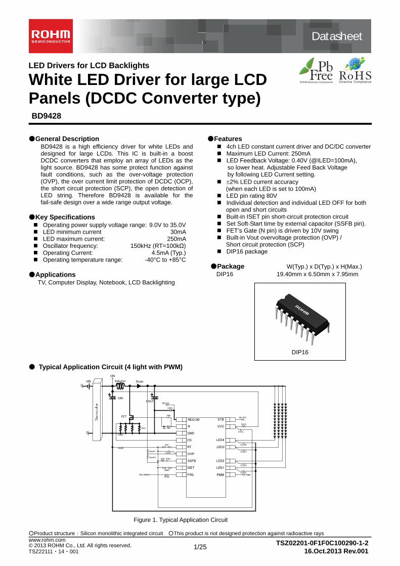
Datasheet ○Product structure:Silicon monolithic integrated circuit ○This product is not designed protection against radioactive rays . 1/25 TSZ02201-0F1F0C100290-1-2 © 2013 ROHM Co., Ltd. All rights reserved. 16.Oct.2013 Rev.001 TSZ22111・14・001 www.rohm.com PWM OVP LED1 LED2 ISET VCC STB RT SSFB LED4 LED3 REG100 N GND CS FAIL PWM PGND REG100 VIN REG100 ON/OFF CREG RN1 RN2 DN RCS RRT ROVP1 ROVP2 COVP RFB CFB1 RFAIL RISET CVCC RVCC Inductor COUT Diode FET AGND CIN VIN CLED4 CLED3 CLED2 CLED1 LED Drivers for LCD Backlights White LED Driver for large LCD Panels (DCDC Converter type) BD9428 ●General Description BD9428 is a high efficiency driver for white LEDs and designed for large LCDs. This IC is built-in a boost DCDC converters that employ an array of LEDs as the light source. BD9428 has some protect function against fault conditions, such as the over-voltage protection (OVP), the over current limit protection of DCDC (OCP), the short circuit protection (SCP), the open detection of LED string. Therefore BD9428 is available for the fail-safe design over a wide range output voltage. ●Key Specifications Operating power supply voltage range: 9.0V to 35.0V LED minimum current 30mA LED maximum current: 250mA Oscillator frequency: 150kHz (RT=100kΩ) Operating Current: 4.5mA (Typ.) Operating temperature range: -40°C to +85°C ●Applications TV, Computer Display, Notebook, LCD Backlighting ●Features 4ch LED constant current driver and DC/DC converter Maximum LED Current: 250mA LED Feedback Voltage: 0.40V (@ILED=100mA), so lower heat. Adjustable Feed Back Voltage by following LED Current setting. 2% LED current accuracy (when each LED is set to 100mA) LED pin rating 80V Individual detection and individual LED OFF for both open and short circuits Built-in ISET pin short-circuit protection circuit Set Soft-Start time by external capacitor (SSFB pin). FET’s Gate (N pin) is driven by 10V swing Built-in Vout overvoltage protection (OVP) / Short circuit protection (SCP) DIP16 package ●Package W(Typ.) x D(Typ.) x H(Max.) DIP16 19.40mm x 6.50mm x 7.95mm ● Typical Application Circuit (4 light with PWM) Figure 1. Typical Application Circuit DIP16
Transcript of LED Drivers for LCD Backlights White LED Driver for large...
Datasheet
Product structure:Silicon monolithic integrated circuit This product is not designed protection against radioactive rays .
1/25
TSZ02201-0F1F0C100290-1-2© 2013 ROHM Co., Ltd. All rights reserved. 16.Oct.2013 Rev.001TSZ22111・14・001
www.rohm.com
PWM
OVP
LED1
LED2
ISET
VCC
STB
RT
SSFB
LED4
LED3
REG100
N
GND
CS
FAIL PWM
PGND
REG100
VIN
REG100
ON/OFF
CREG
RN1
RN2
DNRCS
RRT
ROVP1
ROVP2
COVP
RFB CFB1
RFAIL
RISET
CVCC
RVCC
Inductor
COUT
Diode
FET
AGND
CIN
VIN
CLED4
CLED3
CLED2
CLED1
LED Drivers for LCD Backlights
White LED Driver for large LCD Panels (DCDC Converter type) BD9428
General Description
BD9428 is a high efficiency driver for white LEDs and designed for large LCDs. This IC is built-in a boost DCDC converters that employ an array of LEDs as the light source. BD9428 has some protect function against fault conditions, such as the over-voltage protection (OVP), the over current limit protection of DCDC (OCP), the short circuit protection (SCP), the open detection of LED string. Therefore BD9428 is available for the fail-safe design over a wide range output voltage.
Key Specifications Operating power supply voltage range: 9.0V to 35.0V LED minimum current 30mA LED maximum current: 250mA Oscillator frequency: 150kHz (RT=100kΩ) Operating Current: 4.5mA (Typ.) Operating temperature range: -40°C to +85°C
Applications
TV, Computer Display, Notebook, LCD Backlighting
Features 4ch LED constant current driver and DC/DC converter Maximum LED Current: 250mA LED Feedback Voltage: 0.40V (@ILED=100mA),
so lower heat. Adjustable Feed Back Voltage by following LED Current setting.
2% LED current accuracy (when each LED is set to 100mA)
LED pin rating 80V Individual detection and individual LED OFF for both
open and short circuits Built-in ISET pin short-circuit protection circuit Set Soft-Start time by external capacitor (SSFB pin). FET’s Gate (N pin) is driven by 10V swing Built-in Vout overvoltage protection (OVP) /
Short circuit protection (SCP) DIP16 package
Package W(Typ.) x D(Typ.) x H(Max.) DIP16 19.40mm x 6.50mm x 7.95mm
Typical Application Circuit (4 light with PWM)
Figure 1. Typical Application Circuit
DIP16
DatasheetDatasheet
2/25
TSZ02201-0F1F0C100290-1-2© 2013 ROHM Co., Ltd. All rights reserved. 16.Oct.2013 Rev.001
www.rohm.com
TSZ22111・15・001
BD9428
GND
CS
N
REG100
FAIL
LED1
LED2
OVP PWM
LED4
LED3
SSFB
RT
STB
ISET
VCC
2
3
4
5
6
7
8
1
15
14
13
12
11
10
9
16
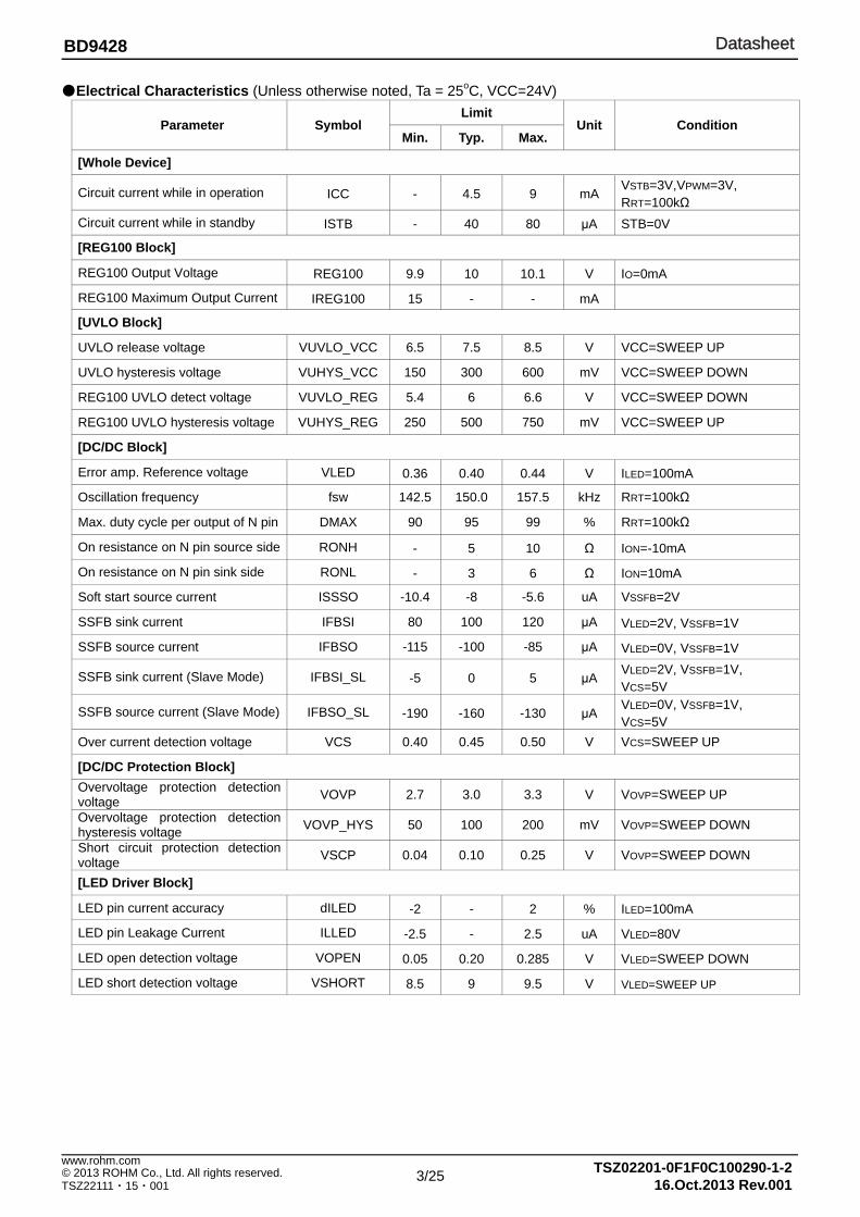
Absolute maximum ratings (Ta=25°C) Parameter Symbol Rating Unit
Power supply voltage VCC 36 V
STB, OVP, PWM, FAIL terminal voltage STB, OVP, PWM, FAIL 36 V
LED1 to 4 terminal voltage LED1 to 4 80 V
CS, ISET, SSFB, RT terminal voltage CS, N, ISET, SSFB, RT 7 V
REG100, N terminal voltage REG100, N 13 V
Power dissipation Pd 1.25 *1 W
Operating temperature range Topr -40~+85 °C
Storage temperature range Tstg -55~+150 °C
Junction temperature Tjmax 150 °C *1 Ta = 25°C or more, diminished at -10mW/°C
Operating Ratings (Ta = 25°C)
Parameter Symbol Limits Unit
VCC supply voltage VCC 9.0 to 35.0 V
Min. output current of LED1 to 4 ILED_MIN 30 mA *1
Max. output current of LED1 to 4 ILED_MAX 250 mA *1,2
DC/DC oscillation frequency fsw 100 to 800 kHz Min. on-duty time for PWM light modulation 1 (under soft-start)
PWM_MIN 1 30 us
Min. on-duty time for PWM light modulation 2 (after soft-start)
PWM_MIN 2 5 us
*1 The amount of current per channel. *2 If LED makes significant variations in its reference voltage, the driver will increase power dissipation, resulting in a rise in package temperature.
To avoid this problem, design the board with thorough consideration given to heat radiation measures.
Pin Configurations Marking Diagram and Physical Dimension
(TOP VIEW) (TOP VIEW)
LOT No.
BD9428
Figure 2. Pin Configuration Figure 3. Marking Diagram and Physical Dimension
DatasheetDatasheet
3/25
TSZ02201-0F1F0C100290-1-2© 2013 ROHM Co., Ltd. All rights reserved. 16.Oct.2013 Rev.001
www.rohm.com
TSZ22111・15・001
BD9428
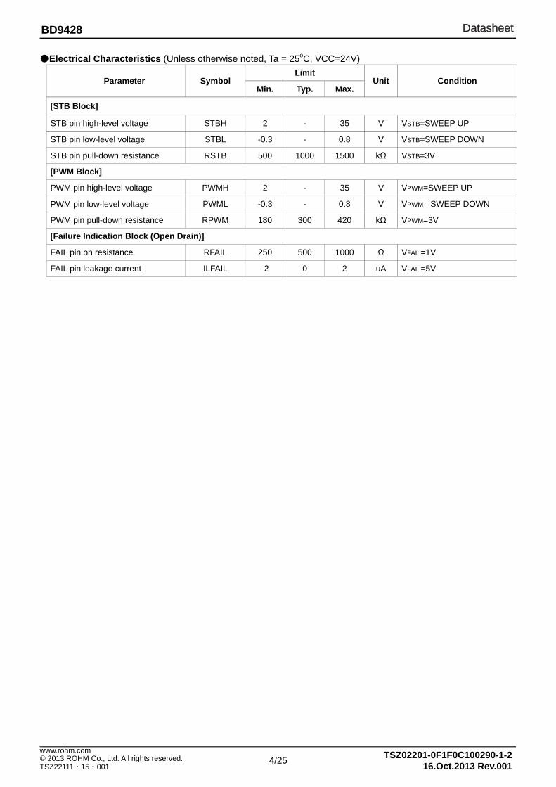
Electrical Characteristics (Unless otherwise noted, Ta = 25oC, VCC=24V)
Parameter Symbol Limit
Unit Condition Min. Typ. Max.
[Whole Device]
Circuit current while in operation ICC - 4.5 9 mA VSTB=3V,VPWM=3V, RRT=100kΩ
Circuit current while in standby ISTB - 40 80 μA STB=0V
[REG100 Block]
REG100 Output Voltage REG100 9.9 10 10.1 V IO=0mA
REG100 Maximum Output Current IREG100 15 - - mA
[UVLO Block]
UVLO release voltage VUVLO_VCC 6.5 7.5 8.5 V VCC=SWEEP UP
UVLO hysteresis voltage VUHYS_VCC 150 300 600 mV VCC=SWEEP DOWN
REG100 UVLO detect voltage VUVLO_REG 5.4 6 6.6 V VCC=SWEEP DOWN
REG100 UVLO hysteresis voltage VUHYS_REG 250 500 750 mV VCC=SWEEP UP
[DC/DC Block]
Error amp. Reference voltage VLED 0.36 0.40 0.44 V ILED=100mA
Oscillation frequency fsw 142.5 150.0 157.5 kHz RRT=100kΩ
Max. duty cycle per output of N pin DMAX 90 95 99 % RRT=100kΩ
On resistance on N pin source side RONH - 5 10 Ω ION=-10mA
On resistance on N pin sink side RONL - 3 6 Ω ION=10mA
Soft start source current ISSSO -10.4 -8 -5.6 uA VSSFB=2V
SSFB sink current IFBSI 80 100 120 μA VLED=2V, VSSFB=1V
SSFB source current IFBSO -115 -100 -85 μA VLED=0V, VSSFB=1V
SSFB sink current (Slave Mode) IFBSI_SL -5 0 5 μA VLED=2V, VSSFB=1V, VCS=5V
SSFB source current (Slave Mode) IFBSO_SL -190 -160 -130 μA VLED=0V, VSSFB=1V, VCS=5V
Over current detection voltage VCS 0.40 0.45 0.50 V VCS=SWEEP UP
[DC/DC Protection Block]
Overvoltage protection detection voltage
VOVP 2.7 3.0 3.3 V VOVP=SWEEP UP
Overvoltage protection detection hysteresis voltage
VOVP_HYS 50 100 200 mV VOVP=SWEEP DOWN
Short circuit protection detection voltage
VSCP 0.04 0.10 0.25 V VOVP=SWEEP DOWN
[LED Driver Block]
LED pin current accuracy dILED -2 - 2 % ILED=100mA
LED pin Leakage Current ILLED -2.5 - 2.5 uA VLED=80V
LED open detection voltage VOPEN 0.05 0.20 0.285 V VLED=SWEEP DOWN
LED short detection voltage VSHORT 8.5 9 9.5 V VLED=SWEEP UP
DatasheetDatasheet
4/25
TSZ02201-0F1F0C100290-1-2© 2013 ROHM Co., Ltd. All rights reserved. 16.Oct.2013 Rev.001
www.rohm.com
TSZ22111・15・001
BD9428
Electrical Characteristics (Unless otherwise noted, Ta = 25oC, VCC=24V)
Parameter Symbol Limit
Unit Condition Min. Typ. Max.
[STB Block]
STB pin high-level voltage STBH 2 - 35 V VSTB=SWEEP UP
STB pin low-level voltage STBL -0.3 - 0.8 V VSTB=SWEEP DOWN
STB pin pull-down resistance RSTB 500 1000 1500 kΩ VSTB=3V
[PWM Block]
PWM pin high-level voltage PWMH 2 - 35 V VPWM=SWEEP UP
PWM pin low-level voltage PWML -0.3 - 0.8 V VPWM= SWEEP DOWN
PWM pin pull-down resistance RPWM 180 300 420 kΩ VPWM=3V
[Failure Indication Block (Open Drain)]
FAIL pin on resistance RFAIL 250 500 1000 Ω VFAIL=1V
FAIL pin leakage current ILFAIL -2 0 2 uA VFAIL=5V
DatasheetDatasheet
5/25
TSZ02201-0F1F0C100290-1-2© 2013 ROHM Co., Ltd. All rights reserved. 16.Oct.2013 Rev.001
www.rohm.com
TSZ22111・15・001
BD9428
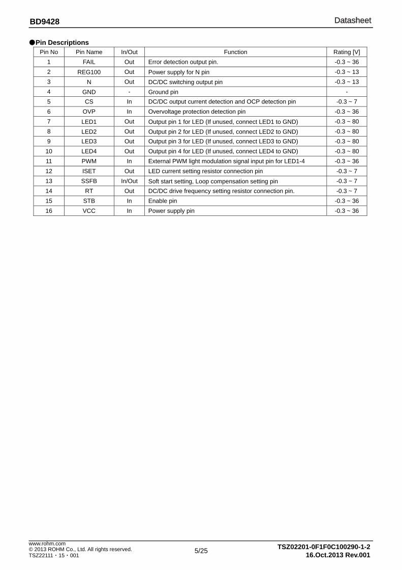
Pin Descriptions Pin No Pin Name In/Out Function Rating [V]
1 FAIL Out Error detection output pin. -0.3 ~ 36
2 REG100 Out Power supply for N pin -0.3 ~ 13
3 N Out DC/DC switching output pin -0.3 ~ 13
4 GND - Ground pin -
5 CS In DC/DC output current detection and OCP detection pin -0.3 ~ 7
6 OVP In Overvoltage protection detection pin -0.3 ~ 36
7 LED1 Out Output pin 1 for LED (If unused, connect LED1 to GND) -0.3 ~ 80
8 LED2 Out Output pin 2 for LED (If unused, connect LED2 to GND) -0.3 ~ 80
9 LED3 Out Output pin 3 for LED (If unused, connect LED3 to GND) -0.3 ~ 80
10 LED4 Out Output pin 4 for LED (If unused, connect LED4 to GND) -0.3 ~ 80
11 PWM In External PWM light modulation signal input pin for LED1-4 -0.3 ~ 36
12 ISET Out LED current setting resistor connection pin -0.3 ~ 7
13 SSFB In/Out Soft start setting, Loop compensation setting pin -0.3 ~ 7
14 RT Out DC/DC drive frequency setting resistor connection pin. -0.3 ~ 7
15 STB In Enable pin -0.3 ~ 36
16 VCC In Power supply pin -0.3 ~ 36
DatasheetDatasheet
6/25
TSZ02201-0F1F0C100290-1-2© 2013 ROHM Co., Ltd. All rights reserved. 16.Oct.2013 Rev.001
www.rohm.com
TSZ22111・15・001
BD9428
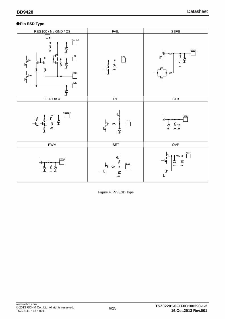
Pin ESD Type
Figure 4. Pin ESD Type
REG100 / N / GND / CS FAIL SSFB
N
GND
CS
REG100
FAIL
SSFB
LED1 to 4 RT STB
LED1-4
RT
STB
PWM ISET OVP
PWM
ISET
OVP
DatasheetDatasheet
7/25
TSZ02201-0F1F0C100290-1-2© 2013 ROHM Co., Ltd. All rights reserved. 16.Oct.2013 Rev.001
www.rohm.com
TSZ22111・15・001
BD9428
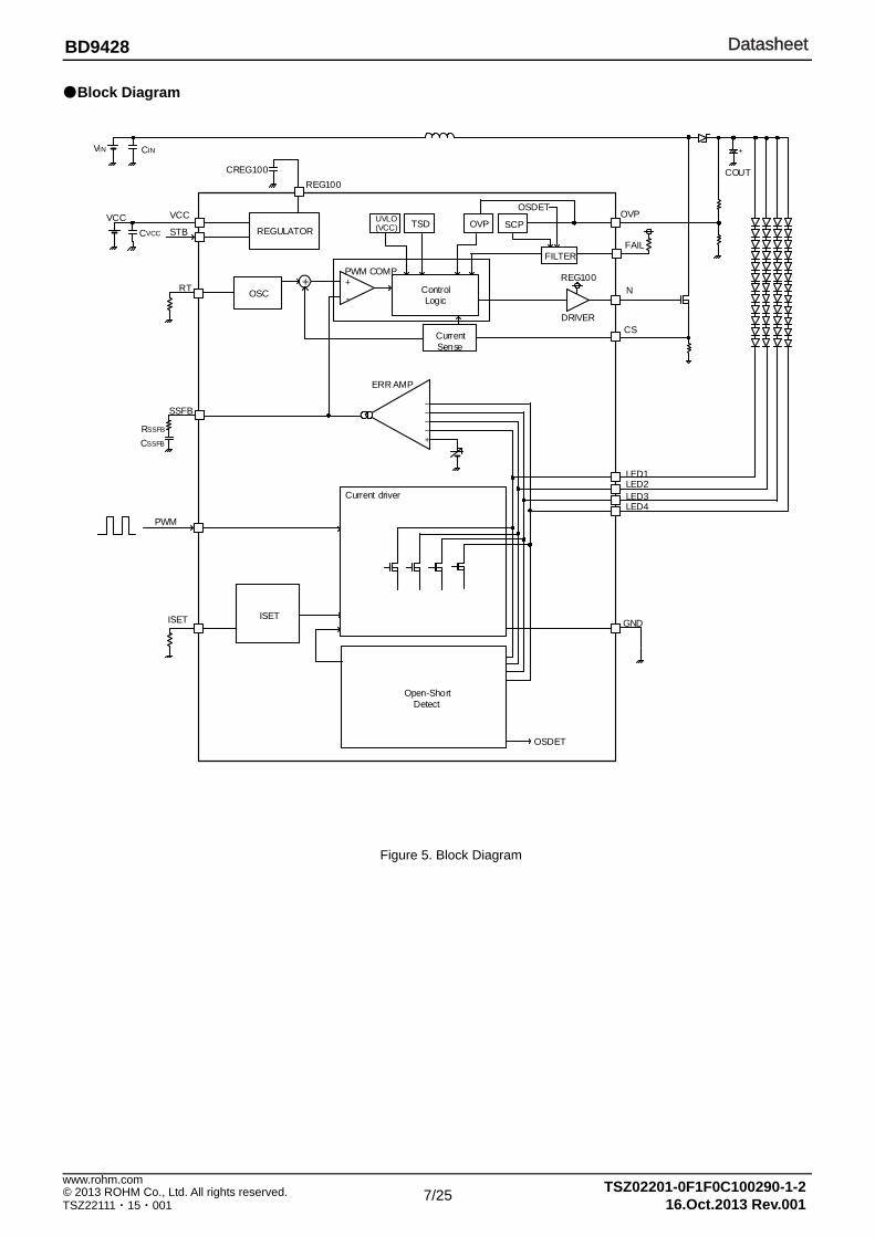
REGULATORSCP
ControlLogic
CurrentSense
+
+----
PWM COMP
DRIVER
ERR AMP
Current driver
VCC
STB
SSFB
CS
N
OVP
REG100
RSSFB
CSSFB
CVCC
VCC
COUT
LED4LED3LED2LED1
OSCRT
UVLO(VCC)
CREG100
+
Open-ShortDetect
ISET
OSDET
+-
VIN CIN
OSDET
ISET GND
TSD OVP
PWM
REG100
FAILFILTER
Block Diagram
Figure 5. Block Diagram
DatasheetDatasheet
8/25
TSZ02201-0F1F0C100290-1-2© 2013 ROHM Co., Ltd. All rights reserved. 16.Oct.2013 Rev.001
www.rohm.com
TSZ22111・15・001
BD9428
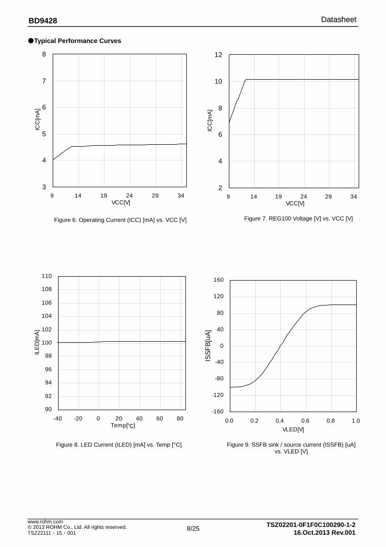
Typical Performance Curves
2
4
6
8
10
12
9 14 19 24 29 34VCC[V]
ICC
[mA
]
Figure 7. REG100 Voltage [V] vs. VCC [V]
90
92
94
96
98
100
102
104
106
108
110
-40 -20 0 20 40 60 80Temp[]
ILE
D[m
A]
-160
-120
-80
-40
0
40
80
120
160
0.0 0.2 0.4 0.6 0.8 1.0
VLED[V]
ISS
FB
[uA
]
3
4
5
6
7
8
9 14 19 24 29 34VCC[V]
ICC
[mA
]
Figure 6. Operating Current (ICC) [mA] vs. VCC [V]
Figure 8. LED Current (ILED) [mA] vs. Temp [°C] Figure 9. SSFB sink / source current (ISSFB) [uA] vs. VLED [V]
DatasheetDatasheet
9/25
TSZ02201-0F1F0C100290-1-2© 2013 ROHM Co., Ltd. All rights reserved. 16.Oct.2013 Rev.001
www.rohm.com
TSZ22111・15・001
BD9428
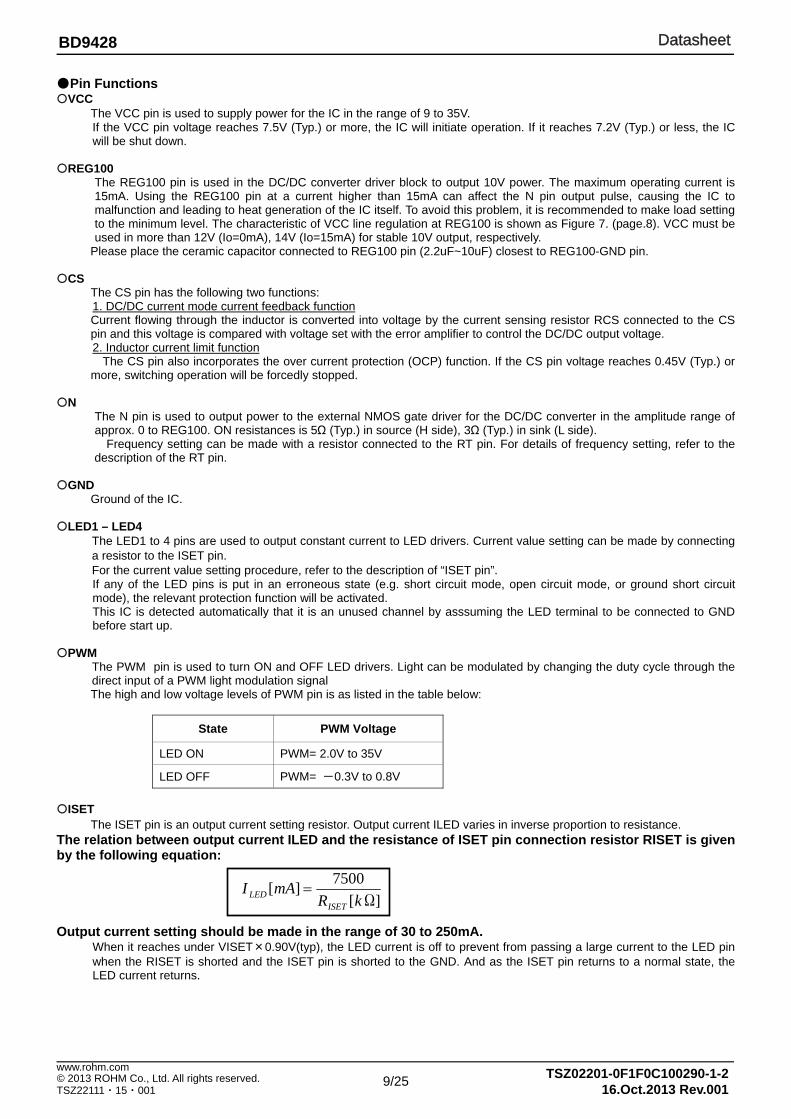
Pin Functions VCC
The VCC pin is used to supply power for the IC in the range of 9 to 35V. If the VCC pin voltage reaches 7.5V (Typ.) or more, the IC will initiate operation. If it reaches 7.2V (Typ.) or less, the IC will be shut down.
REG100
The REG100 pin is used in the DC/DC converter driver block to output 10V power. The maximum operating current is 15mA. Using the REG100 pin at a current higher than 15mA can affect the N pin output pulse, causing the IC to malfunction and leading to heat generation of the IC itself. To avoid this problem, it is recommended to make load setting to the minimum level. The characteristic of VCC line regulation at REG100 is shown as Figure 7. (page.8). VCC must be used in more than 12V (Io=0mA), 14V (Io=15mA) for stable 10V output, respectively.
Please place the ceramic capacitor connected to REG100 pin (2.2uF~10uF) closest to REG100-GND pin. CS
The CS pin has the following two functions: 1. DC/DC current mode current feedback function Current flowing through the inductor is converted into voltage by the current sensing resistor RCS connected to the CS pin and this voltage is compared with voltage set with the error amplifier to control the DC/DC output voltage. 2. Inductor current limit function
The CS pin also incorporates the over current protection (OCP) function. If the CS pin voltage reaches 0.45V (Typ.) or more, switching operation will be forcedly stopped.
N
The N pin is used to output power to the external NMOS gate driver for the DC/DC converter in the amplitude range of approx. 0 to REG100. ON resistances is 5Ω (Typ.) in source (H side), 3Ω (Typ.) in sink (L side).
Frequency setting can be made with a resistor connected to the RT pin. For details of frequency setting, refer to the description of the RT pin.
GND
Ground of the IC. LED1 – LED4
The LED1 to 4 pins are used to output constant current to LED drivers. Current value setting can be made by connecting a resistor to the ISET pin. For the current value setting procedure, refer to the description of “ISET pin”. If any of the LED pins is put in an erroneous state (e.g. short circuit mode, open circuit mode, or ground short circuit mode), the relevant protection function will be activated. This IC is detected automatically that it is an unused channel by asssuming the LED terminal to be connected to GND before start up.
PWM
The PWM pin is used to turn ON and OFF LED drivers. Light can be modulated by changing the duty cycle through the direct input of a PWM light modulation signal The high and low voltage levels of PWM pin is as listed in the table below:
State PWM Voltage
LED ON PWM= 2.0V to 35V
LED OFF PWM= -0.3V to 0.8V
ISET
The ISET pin is an output current setting resistor. Output current ILED varies in inverse proportion to resistance. The relation between output current ILED and the resistance of ISET pin connection resistor RISET is given by the following equation: Output current setting should be made in the range of 30 to 250mA.
When it reaches under VISET×0.90V(typ), the LED current is off to prevent from passing a large current to the LED pin when the RISET is shorted and the ISET pin is shorted to the GND. And as the ISET pin returns to a normal state, the LED current returns.
Ω][
7500][
kRmAI
ISETLED
DatasheetDatasheet
10/25
TSZ02201-0F1F0C100290-1-2© 2013 ROHM Co., Ltd. All rights reserved. 16.Oct.2013 Rev.001
www.rohm.com
TSZ22111・15・001
BD9428
It prepares automatically to suitable LED feedback voltage that can output LED current set by ISET pin. In short LED feedback voltage is dropped when the LED current is small and the IC heating is held automatically. In case of a large current is needed, raise the LED pin feedback voltage. And it adjusts automatically to LED pin voltage that can be flow large LED current. The calculation is as below. The LED feedback voltage (VLED) is clamped to 0.40V (Typ.) when the LED current (ILED) is less than 133.3mA.
SSFB
The SSFB pin is used to make setting of soft start time and duty for soft start, and DC/DC current mode control error amplifier. It performs constant current charge of 8 uA to the external capacitor connected to SSFB terminal, which enables soft-start of DC/DC converter. The SSFB pin detects the voltages of LED pins (1 to 4) and controls inductor current so that the pin voltage of the LED located in the row with the highest Vf will come to 0.40V (ILED=100mA). As a result, the pin voltages of other LEDs become higher by Vf variation. After completion of soft start, the SSFB pin is put into the high-impedance state with the PWM signal being in the low state, thus maintaining the SSFB voltage. Since the LED protection function (OPEN/SHORT detection) works when it turns to the LED feedback mode.
RT
The RT pin is used to connect a DC/DC frequency setting resistor. DC/DC drive frequency is determined by connecting
the RT resistor. Drive frequency vs. RT resistance (Ideal)
When RT is 100kΩ, Fsw is 150kHz(Typ.). However, drive frequency setting should be made in the range of 100 kHz to 800 kHz.
OVP
The OVP pin is an input pin for over-voltage protection and short circuit protection of DC/DC output voltage. If over-voltage is detected, the OVP pin will stop the DC/DC converter conducting step-up operation. When the short circuit protection (SCP) function is activated, the DC/DC converter will stop operation, and then the timer will start counting. When the timer completes counting the preset period of time, the LED drivers are stopped. The OVP pin is of the high impedance type and involves no pull-down resistor, resulting in unstable potential in the open-circuited state. To avoid this problem, be sure to make input voltage setting with the use of a resistive divider or otherwise.
STB
The STB pin is used to make setting of turning ON and OFF the IC and allowed for use to reset the IC from shutdown. Note: The IC state is switched (i.e., the IC is switched between ON and OFF state) according to voltages input in the STB pin. Avoid using the STB pin between two states (0.8 to 2.0V).
FAIL
This FAIL pin is used to output FAIL signal (open drain). If any error is detected, NMOS will be put into the open-circuited state. If no LED pin is used, LED pin processing will be conducted in the open-circuited state, LED_OPEN protection will be detected to output the OPEN signal from the FAIL pin.
STATE FAIL Signal Output
Normal operation GND Level
Error detection (after timer is latched) OPEN
][][
15000 k
kHzfR
SWRT
][][0.3 VAIVLED LED
DatasheetDatasheet
11/25
TSZ02201-0F1F0C100290-1-2© 2013 ROHM Co., Ltd. All rights reserved. 16.Oct.2013 Rev.001
www.rohm.com
TSZ22111・15・001
BD9428
STB
ILED
LED_OK
①
OSC
Soft-Start(ISS=8uA) IFB(Sink, Source)=±100uA)
SSFB
PWM
N
VOUT
②
③
④
⑤⑥
LED_OK
SSFB
5V
0.4V
LED_DRIVER
OSC
DRIVER
COMPN
LED
VOUT
ILE
D
PWM
PW
M=
L:S
TO
P
8uA
DQPWM
CS
CSSFB
RS SFB
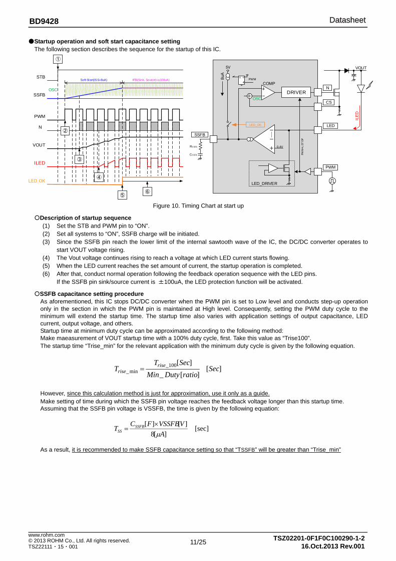
Startup operation and soft start capacitance setting The following section describes the sequence for the startup of this IC.
Description of startup sequence (1) Set the STB and PWM pin to “ON”. (2) Set all systems to “ON”, SSFB charge will be initiated. (3) Since the SSFB pin reach the lower limit of the internal sawtooth wave of the IC, the DC/DC converter operates to
start VOUT voltage rising. (4) The Vout voltage continues rising to reach a voltage at which LED current starts flowing. (5) When the LED current reaches the set amount of current, the startup operation is completed. (6) After that, conduct normal operation following the feedback operation sequence with the LED pins.
If the SSFB pin sink/source current is ±100uA, the LED protection function will be activated.
SSFB capacitance setting procedure As aforementioned, this IC stops DC/DC converter when the PWM pin is set to Low level and conducts step-up operation only in the section in which the PWM pin is maintained at High level. Consequently, setting the PWM duty cycle to the minimum will extend the startup time. The startup time also varies with application settings of output capacitance, LED current, output voltage, and others. Startup time at minimum duty cycle can be approximated according to the following method: Make maeasurement of VOUT startup time with a 100% duty cycle, first. Take this value as “Trise100”. The startup time “Trise_min” for the relevant application with the minimum duty cycle is given by the following equation.
][][_
][100_min_ Sec
ratioDutyMin
SecTT rise
rise
However, since this calculation method is just for approximation, use it only as a guide. Make setting of time during which the SSFB pin voltage reaches the feedback voltage longer than this startup time. Assuming that the SSFB pin voltage is VSSFB, the time is given by the following equation:
[sec]][8
][][
A
VVSSFBFCT SSFB
SS
As a result, it is recommended to make SSFB capacitance setting so that “TSSFB” will be greater than “Trise_min”
Figure 10. Timing Chart at start up
DatasheetDatasheet
12/25
TSZ02201-0F1F0C100290-1-2© 2013 ROHM Co., Ltd. All rights reserved. 16.Oct.2013 Rev.001
www.rohm.com
TSZ22111・15・001
BD9428
][][
15000 k
kHzfR
SWRT
LED current setting Setting of LED output current “ILED” can be made by connecting a resistor RISET to the ISET pin.
RISET vs. ILED current relation equation
However, LED current setting should be made in the range of 30mA to 150mA.
[Setting example] To set ILED current to 100mA, RISET resistance is given by the following equation:
DC/DC converter drive frequency setting
DC/DC converter drive frequency is determined by making RT resistance setting.
Drive frequency vs. RT resistance (ideal) relation equation
[Setting example] To set DC/DC drive frequency “fsw” to 200 kHz, RRT is given by the following equation:
][][
7500 k
mAIR
LEDISET
][75][100
7500
][
7500 k
mAmAIR
LEDISET
where fsw DC/DC converter oscillation frequency [kHz]
This equation has become an ideal equation without any correction item included. For accurate frequency settings, thorough verification should be performed on practical sets.
][75][200
15000
][
15000 k
kHzkHzfR
swRT
DatasheetDatasheet
13/25
TSZ02201-0F1F0C100290-1-2© 2013 ROHM Co., Ltd. All rights reserved. 16.Oct.2013 Rev.001
www.rohm.com
TSZ22111・15・001
BD9428
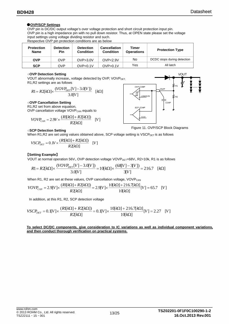
OVP
VOUT
2.9V/3.0V
+
-
+
-
OVP COMP
0.1V
R2
R1
SCP COMP
COVP
OVP/SCP Settings OVP pin is DC/DC output voltage’s over voltage protection and short circuit protection input pin. OVP pin is a high impedance pin with no pull down resistor. Thus, at OPEN state please set the voltage input settings using voltage dividing resistor and such. Respective OVP pin protection conditions are as below
Protection Name
Detection Pin
Detection Condition
Cancellation Condition
Timer Operations
Protection Type
OVP OVP OVP>3.0V OVP<2.9V No DCDC stops during detection
SCP OVP OVP<0.1V OVP>0.1V Yes All latch
OVP Detection Setting VOUT abnormally increase、voltage detected by OVP, VOVPDET, R1,R2 settings are as follows OVP Cancellation Setting R1,R2 set from above equation, OVP cancellation voltage VOVPCAN equals to SCP Detection Setting When R1,R2 are set using values obtained above, SCP voltage setting is VSCPDET is as follows 【Setting Example】 VOUT at normal operation 56V、OVP detection voltage VOVPDET=68V、R2=10k, R1 is as follows When R1, R2 are set at these values, OVP cancellation voltage, VOVPCAN In addition, at this R1, R2, SCP detection voltage To select DC/DC components, give consideration to IC variations as well as individual component variations, and then conduct thorough verification on practical systems.
][][0.3
])[0.3][(][21
k
V
VVVOVPkRR DET
][][2
])[2][1(9.2 V
kR
kRkRVVOVPCAN
][7.216][3
])[3][68(][10
][0.3
])[0.3][(][21
k
V
VVk
V
VVVOVPkRR DET
][7.65][][10
][7.216][10][9.2
][2
])[2][1(][9.2 VV
k
kkV
kR
kRkRVVOVPCAN
][][2
])[2][1(1.0 V
kR
kRkRVVSCPDET
][27.2][][10
][7.216][10][1.0
][2
])[2][1(][1.0 VV
k
kkV
kR
kRkRVVSCPDET
Figure 11. OVP/SCP Block Diagrams
DatasheetDatasheet
14/25
TSZ02201-0F1F0C100290-1-2© 2013 ROHM Co., Ltd. All rights reserved. 16.Oct.2013 Rev.001
www.rohm.com
TSZ22111・15・001
BD9428
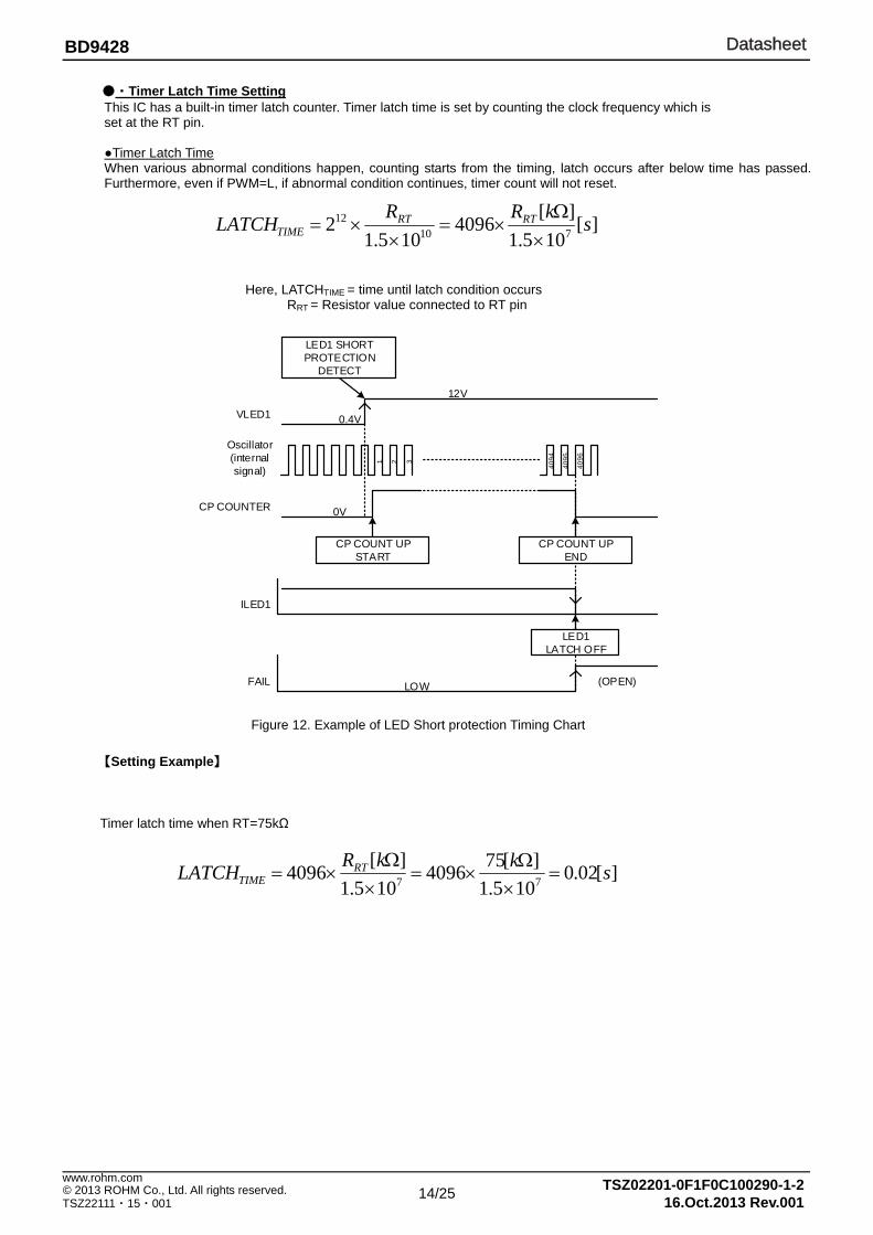
CP COUNT UPSTART
Oscillator(internal signal)
LED1 SHORT PROTECTION
DETECT
FAIL
3
CP COUNT UPEND
LED1LATCH OFF
LOW
ILED1
CP COUNTER 0V
1 2
40
94
40
95
40
96
VLED1 0.4V
12V
(OPEN)
・Timer Latch Time Setting This IC has a built-in timer latch counter. Timer latch time is set by counting the clock frequency which is set at the RT pin. Timer Latch Time When various abnormal conditions happen, counting starts from the timing, latch occurs after below time has passed. Furthermore, even if PWM=L, if abnormal condition continues, timer count will not reset.
Here, LATCHTIME = time until latch condition occurs RRT = Resistor value connected to RT pin
【Setting Example】
Timer latch time when RT=75kΩ
][105.1
][4096
105.12
71012 s
kRRLATCH RTRT
TIME
Figure 12. Example of LED Short protection Timing Chart
][02.0105.1
][754096
105.1
][4096
77s
kkRLATCH RT
TIME
DatasheetDatasheet
15/25
TSZ02201-0F1F0C100290-1-2© 2013 ROHM Co., Ltd. All rights reserved. 16.Oct.2013 Rev.001
www.rohm.com
TSZ22111・15・001
BD9428
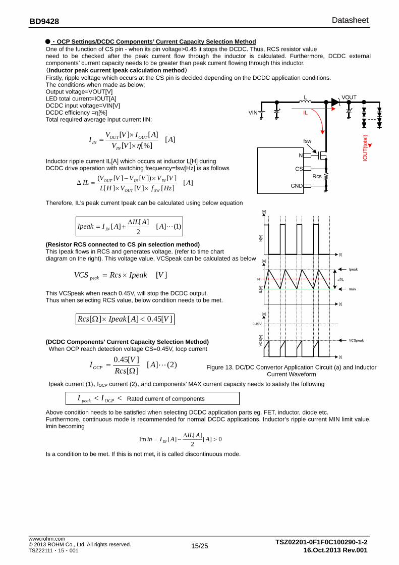
VIN
VOUT
N
CS
GND
Rcs
IL
L
IOU
T(t
otal
)
fsw
0.45V
[V]
VC
S[V
]
VCSpeak
[t]
[t]
IL[A
][A]
Imin
Ipeak
⊿ILIIN
[t]
N[V
]
[V]
・OCP Settings/DCDC Components’ Current Capacity Selection Method One of the function of CS pin - when its pin voltage>0.45 it stops the DCDC. Thus, RCS resistor value need to be checked after the peak current flow through the inductor is calculated. Furthermore, DCDC external components’ current capacity needs to be greater than peak current flowing through this inductor. (Inductor peak current Ipeak calculation method) Firstly, ripple voltage which occurs at the CS pin is decided depending on the DCDC application conditions. The conditions when made as below; Output voltage=VOUT[V] LED total current=IOUT[A] DCDC input voltage=VIN[V] DCDC efficiency =η[%] Total required average input current IIN: Inductor ripple current IL[A] which occurs at inductor L[H] during DCDC drive operation with switching frequency=fsw[Hz] is as follows Therefore, IL’s peak current Ipeak can be calculated using below equation (Resistor RCS connected to CS pin selection method) This Ipeak flows in RCS and generates voltage. (refer to time chart diagram on the right). This voltage value, VCSpeak can be calculated as below This VCSpeak when reach 0.45V, will stop the DCDC output. Thus when selecting RCS value, below condition needs to be met. (DCDC Components’ Current Capacity Selection Method) When OCP reach detection voltage CS=0.45V, Iocp current Ipeak current (1)、IOCP current (2)、and components’ MAX current capacity needs to satisfy the following Above condition needs to be satisfied when selecting DCDC application parts eg. FET, inductor, diode etc. Furthermore, continuous mode is recommended for normal DCDC applications. Inductor’s ripple current MIN limit value, lmin becoming Is a condition to be met. If this is not met, it is called discontinuous mode.
][[%]][
][][A
VV
AIVVI
IN
OUTOUTIN
][][][][
][])[][(A
HzfVVHL
VVVVVVIL
SWOUT
ININOUT
Δ
)1(][2
][][ A
AILAIIpeak IN
][VIpeakRcsVCS peak
OCPpeak II
)2(][][
][45.0A
Rcs
VIOCP
][45.0][][ VAIpeakRcs
Rated current of components
0][2
][][Im
A
AILAIin IN
Figure 13. DC/DC Convertor Application Circuit (a) and Inductor Current Waveform
DatasheetDatasheet
16/25
TSZ02201-0F1F0C100290-1-2© 2013 ROHM Co., Ltd. All rights reserved. 16.Oct.2013 Rev.001
www.rohm.com
TSZ22111・15・001
BD9428
【Setting Example】 Output voltage=VOUT[V]=56V LED total current=IOUT[A]=100mA×4ch=0.40A DCDC input voltage=VIN[V]=14V DCDC efficiency=η[%]=90% Total required average input current IIN: When, DCDC switching frequency =fsw[Hz]=200kHz Inductor L[H]=33uH, Inductor ripple current ΔIL[A]: Thus, IL peak current Ipeak becomes
RCS resistor value when set at 0.1Ω and satisfy the condition. In addition、OCP detection current IOCP at this time is If parts used (FET,INDUCTOR、DIODE etc)’s current capacity<5A, Thus, there is no problem of parts selection as the above condition is satisfied. In addition、IL ripple current minimum limit Imin is Thus、will not become discontinuous mode。
To select DC/DC components, give consideration to IC variations as well as individual component variations, and then conduct thorough verification on practical systems.
][78.1[%]90][14
][40.0][56
[%]][
][][][ A
V
AV
VV
AIVVAI
IN
OUTOUTIN
][59.1][10200][56][1033
][14])[14][56(
][][][
][])[][(36
AHzVH
VVV
HzfVVHL
VVVVVVIL
SWOUT
ININOUT
Δ
][58.22
][59.1][78.1][
2
][][ A
AAA
AILAIIpeak IN
0][985.0][795.0][78.1][2
][][Im
AAAA
AILAIin IN
VVAIpeakRcsVCS peak 45.0][258.0][58.2][10.0
][5.4][1.0
][45.0A
VIOCP
OCPpeak II Rated current of components ][5][5.4][58.2 AAA
…Peak current calculation result
…RCS resistor consideration
…DCDC current capacity consideration
DatasheetDatasheet
17/25
TSZ02201-0F1F0C100290-1-2© 2013 ROHM Co., Ltd. All rights reserved. 16.Oct.2013 Rev.001
www.rohm.com
TSZ22111・15・001
BD9428
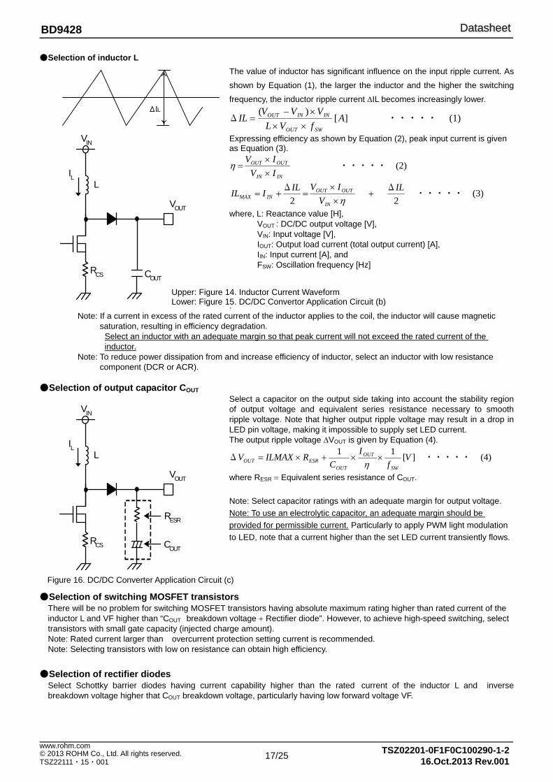
Selection of inductor L
The value of inductor has significant influence on the input ripple current. As
shown by Equation (1), the larger the inductor and the higher the switching
frequency, the inductor ripple current ∆IL becomes increasingly lower.
(1)][)(
・・・・・ Δ AfVL
VVVIL
SWOUT
ININOUT
Expressing efficiency as shown by Equation (2), peak input current is given as Equation (3).
(2) ・・・・・ININ
OUTOUT
IV
IV
(3)22
・・・・・ Δ
Δ IL
V
IVILIIL
IN
OUTOUTINMAX
where, L: Reactance value [H], VOUT : DC/DC output voltage [V], VIN: Input voltage [V], IOUT: Output load current (total output current) [A], IIN: Input current [A], and FSW: Oscillation frequency [Hz] .
Note: If a current in excess of the rated current of the inductor applies to the coil, the inductor will cause magnetic saturation, resulting in efficiency degradation.
Select an inductor with an adequate margin so that peak current will not exceed the rated current of the inductor.
Note: To reduce power dissipation from and increase efficiency of inductor, select an inductor with low resistance component (DCR or ACR).
Selection of output capacitor COUT
Select a capacitor on the output side taking into account the stability region of output voltage and equivalent series resistance necessary to smooth ripple voltage. Note that higher output ripple voltage may result in a drop in LED pin voltage, making it impossible to supply set LED current. The output ripple voltage ∆VOUT is given by Equation (4).
(4)][11
・・・・・ Δ Vf
I
CRILMAXV
SW
OUT
OUTESROUT
where RESR Equivalent series resistance of COUT.
Note: Select capacitor ratings with an adequate margin for output voltage.
Note: To use an electrolytic capacitor, an adequate margin should be
provided for permissible current. Particularly to apply PWM light modulation
to LED, note that a current higher than the set LED current transiently flows.
Selection of switching MOSFET transistors
There will be no problem for switching MOSFET transistors having absolute maximum rating higher than rated current of the inductor L and VF higher than “COUT breakdown voltage Rectifier diode”. However, to achieve high-speed switching, select transistors with small gate capacity (injected charge amount). Note: Rated current larger than overcurrent protection setting current is recommended. Note: Selecting transistors with low on resistance can obtain high efficiency.
Selection of rectifier diodes Select Schottky barrier diodes having current capability higher than the rated current of the inductor L and inverse breakdown voltage higher that COUT breakdown voltage, particularly having low forward voltage VF.
ΔIL
VOUT
VIN
COUTRCS
LIL
VOUT
VIN
COUTRCS
L
RESR
IL
Upper: Figure 14. Inductor Current Waveform Lower: Figure 15. DC/DC Convertor Application Circuit (b)
Figure 16. DC/DC Converter Application Circuit (c)
DatasheetDatasheet
18/25
TSZ02201-0F1F0C100290-1-2© 2013 ROHM Co., Ltd. All rights reserved. 16.Oct.2013 Rev.001
www.rohm.com
TSZ22111・15・001
BD9428
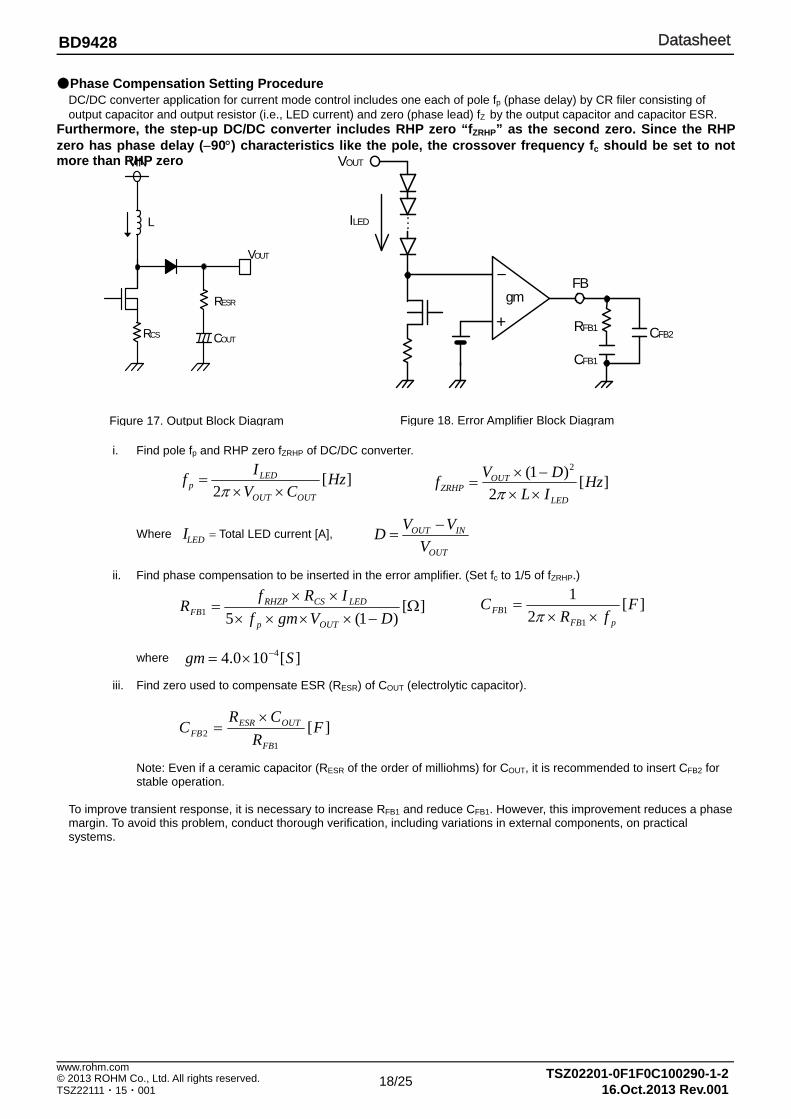
Phase Compensation Setting Procedure DC/DC converter application for current mode control includes one each of pole fp (phase delay) by CR filer consisting of output capacitor and output resistor (i.e., LED current) and zero (phase lead) fZ by the output capacitor and capacitor ESR.
Furthermore, the step-up DC/DC converter includes RHP zero “fZRHP” as the second zero. Since the RHP zero has phase delay (90) characteristics like the pole, the crossover frequency fc should be set to not more than RHP zero
i. Find pole fp and RHP zero fZRHP of DC/DC converter. Where Total LED current [A], ii. Find phase compensation to be inserted in the error amplifier. (Set fc to 1/5 of fZRHP.)
where iii. Find zero used to compensate ESR (RESR) of COUT (electrolytic capacitor).
Note: Even if a ceramic capacitor (RESR of the order of milliohms) for COUT, it is recommended to insert CFB2 for stable operation.
To improve transient response, it is necessary to increase RFB1 and reduce CFB1. However, this improvement reduces a phase margin. To avoid this problem, conduct thorough verification, including variations in external components, on practical systems.
VOUT
VIN
COUTRCS
L
RESR
+
-
CFB1
FB
RFB1
gm
VOUT
ILED
CFB2
Figure 17. Output Block Diagram Figure 18. Error Amplifier Block Diagram
][2
)1( 2
HzIL
DVf
LED
OUTZRHP
][)1(51
DVgmf
IRfR
OUTp
LEDCSRHZPFB
][2
1
11 F
fRC
pFBFB
][1
2 FR
CRC
FB
OUTESRFB
][2
HzCV
If
OUTOUT
LEDp
OUT
INOUT
V
VVD
][100.4 4 Sgm
LEDI
DatasheetDatasheet
19/25
TSZ02201-0F1F0C100290-1-2© 2013 ROHM Co., Ltd. All rights reserved. 16.Oct.2013 Rev.001
www.rohm.com
TSZ22111・15・001
BD9428
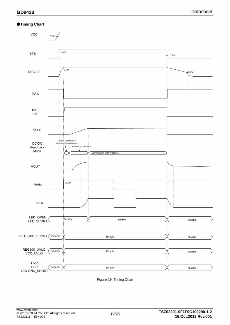
7.5V
STB
VCC
REG100
ISETRT
SSFB
DC/DCFeedback
Mode
VOUT
PWM
ILEDx
LED_OPEN LED_SHORT
OVPSCP
LED GND_SHORT
Disable Enable
ISET_GND_SHORT
REG100_UVLOVCC_UVLO
EnableDisable
Disable
2.0V
6.5V
Soft-start (ISSFB=8uA)
LED feedback (ISSFB=±100uA)
FAIL
2.0V
Disable
EnableDisable Disable
EnableDisable Disable
Unused LED channelAuto-detection sequence
0.8V
6.0V
Timing Chart
Figure 19. Timing Chart
DatasheetDatasheet
20/25
TSZ02201-0F1F0C100290-1-2© 2013 ROHM Co., Ltd. All rights reserved. 16.Oct.2013 Rev.001
www.rohm.com
TSZ22111・15・001
BD9428
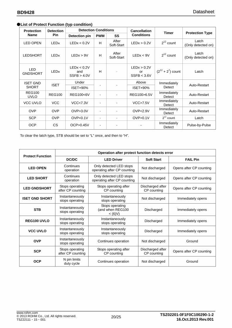
List of Protect Function (typ condition)
Protection Name
Detection Pin
Detection Conditions Cancellation Conditions
Timer Protection TypeDetection pin PWM SS
LED OPEN LEDx LEDx < 0.2V H After
Soft-StartLEDx > 0.2V 212 count
Latch (Only detected on)
LEDSHORT LEDx LEDx > 9V H After
Soft-StartLEDx < 9V 212 count
Latch (Only detected on)
LED GNDSHORT
LEDx LEDx < 0.2V
and SSFB > 4.0V
H -
LEDx > 0.2V or
SSFB < 3.6V (212 + 27) count Latch
ISET GND SHORT
ISET Under
- - Above Immediately
Detect Auto-Restart
ISET×90% ISET×90% REG100 UVLO
REG100 REG100<6V - - REG100>6.5VImmediately
Detect Auto-Restart
VCC UVLO VCC VCC<7.3V - - VCC>7.5V Immediately
Detect Auto-Restart
OVP OVP OVP>3.0V - - OVP<2.9V Immediately
Detect Auto-Restart
SCP OVP OVP<0.1V - - OVP>0.1V 212 count Latch
OCP CS OCP>0.45V - - - Immediately
Detect Pulse-by-Pulse
To clear the latch type, STB should be set to “L” once, and then to “H”.
Protect Function Operation after protect function detects error
DC/DC LED Driver Soft Start FAIL Pin
LED OPEN Continues operation
Only detected LED stops operating after CP counting
Not discharged Opens after CP counting
LED SHORT Continues operation
Only detected LED stops operating after CP counting
Not discharged Opens after CP counting
LED GNDSHORT Stops operating
after CP counting Stops operating after
CP counting Discharged after
CP counting Opens after CP counting
ISET GND SHORT Instantaneously stops operating
Instantaneously stops operating
Not discharged Immediately opens
STB Instantaneously stops operating
Stops operating (and when REG100
< (6)V) Discharged Immediately opens
REG100 UVLO Instantaneously stops operating
Instantaneously stops operating
Discharged Immediately opens
VCC UVLO Instantaneously stops operating
Instantaneously stops operating
Discharged Immediately opens
OVP Instantaneously stops operating
Continues operation Not discharged Ground
SCP Stops operating
after CP counting Stops operating after
CP counting Discharged after
CP counting Opens after CP counting
OCP N pin limits duty cycle
Continues operation Not discharged Ground
DatasheetDatasheet
21/25
TSZ02201-0F1F0C100290-1-2© 2013 ROHM Co., Ltd. All rights reserved. 16.Oct.2013 Rev.001
www.rohm.com
TSZ22111・15・001
BD9428
Operational Notes
1. Reverse Connection of Power Supply Connecting the power supply in reverse polarity can damage the IC. Take precautions against reverse polarity when connecting the power supply, such as mounting an external diode between the power supply and the IC’s power supply terminals.
2. Power Supply Lines Design the PCB layout pattern to provide low impedance supply lines. Separate the ground and supply lines of the digital and analog blocks to prevent noise in the ground and supply lines of the digital block from affecting the analog block. Furthermore, connect a capacitor to ground at all power supply pins. Consider the effect of temperature and aging on the capacitance value when using electrolytic capacitors.
3. Ground Voltage
Ensure that no pins are at a voltage below that of the ground pin at any time, even during transient condition.
4. Ground Wiring Pattern When using both small-signal and large-current ground traces, the two ground traces should be routed separately but connected to a single ground at the reference point of the application board to avoid fluctuations in the small-signal ground caused by large currents. Also ensure that the ground traces of external components do not cause variations on the ground voltage. The ground lines must be as short and thick as possible to reduce line impedance.
5. Thermal Consideration
Should by any chance the power dissipation rating be exceeded the rise in temperature of the chip may result in deterioration of the properties of the chip. The absolute maximum rating of the Pd stated in this specification is when the IC is mounted on a 70mm x 70mm x 1.6mm glass epoxy board. In case of exceeding this absolute maximum rating, increase the board size and copper area to prevent exceeding the Pd rating.
6. Recommended Operating Conditions
These conditions represent a range within which the expected characteristics of the IC can be approximately obtained. The electrical characteristics are guaranteed under the conditions of each parameter.
7. Inrush Current
When power is first supplied to the IC, it is possible that the internal logic may be unstable and inrush current may flow instantaneously due to the internal powering sequence and delays, especially if the IC has more than one power supply. Therefore, give special consideration to power coupling capacitance, power wiring, width of ground wiring, and routing of connections.
8. Testing on Application Boards
When testing the IC on an application board, connecting a capacitor directly to a low-impedance output pin may subject the IC to stress. Always discharge capacitors completely after each process or step. The IC’s power supply should always be turned off completely before connecting or removing it from the test setup during the inspection process. To prevent damage from static discharge, ground the IC during assembly and use similar precautions during transport and storage.
9. Inter-pin Short and Mounting Errors Ensure that the direction and position are correct when mounting the IC on the PCB. Incorrect mounting may result in damaging the IC. Avoid nearby pins being shorted to each other especially to ground, power supply and output pin. Inter-pin shorts could be due to many reasons such as metal particles, water droplets (in very humid environment) and unintentional solder bridge deposited in between pins during assembly to name a few.
DatasheetDatasheet
22/25
TSZ02201-0F1F0C100290-1-2© 2013 ROHM Co., Ltd. All rights reserved. 16.Oct.2013 Rev.001
www.rohm.com
TSZ22111・15・001
BD9428
Operational Notes – continued
10. Unused Input Terminals Input terminals of an IC are often connected to the gate of a MOS transistor. The gate has extremely high impedance and extremely low capacitance. If left unconnected, the electric field from the outside can easily charge it. The small charge acquired in this way is enough to produce a significant effect on the conduction through the transistor and cause unexpected operation of the IC. So unless otherwise specified, unused input terminals should be connected to the power supply or ground line.
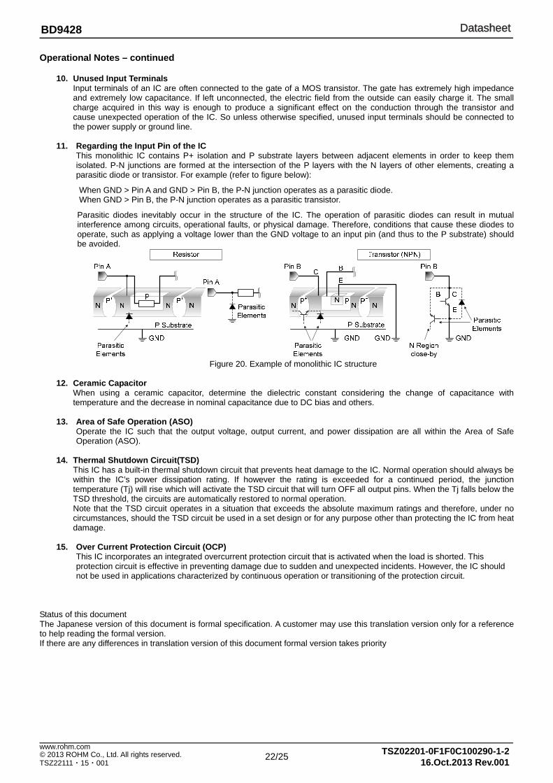
11. Regarding the Input Pin of the IC This monolithic IC contains P+ isolation and P substrate layers between adjacent elements in order to keep them isolated. P-N junctions are formed at the intersection of the P layers with the N layers of other elements, creating a parasitic diode or transistor. For example (refer to figure below):
When GND > Pin A and GND > Pin B, the P-N junction operates as a parasitic diode. When GND > Pin B, the P-N junction operates as a parasitic transistor.
Parasitic diodes inevitably occur in the structure of the IC. The operation of parasitic diodes can result in mutual interference among circuits, operational faults, or physical damage. Therefore, conditions that cause these diodes to operate, such as applying a voltage lower than the GND voltage to an input pin (and thus to the P substrate) should be avoided.
Figure 20. Example of monolithic IC structure
12. Ceramic Capacitor When using a ceramic capacitor, determine the dielectric constant considering the change of capacitance with temperature and the decrease in nominal capacitance due to DC bias and others.
13. Area of Safe Operation (ASO)
Operate the IC such that the output voltage, output current, and power dissipation are all within the Area of Safe Operation (ASO).
14. Thermal Shutdown Circuit(TSD)
This IC has a built-in thermal shutdown circuit that prevents heat damage to the IC. Normal operation should always be within the IC’s power dissipation rating. If however the rating is exceeded for a continued period, the junction temperature (Tj) will rise which will activate the TSD circuit that will turn OFF all output pins. When the Tj falls below the TSD threshold, the circuits are automatically restored to normal operation. Note that the TSD circuit operates in a situation that exceeds the absolute maximum ratings and therefore, under no circumstances, should the TSD circuit be used in a set design or for any purpose other than protecting the IC from heat damage.
15. Over Current Protection Circuit (OCP)
This IC incorporates an integrated overcurrent protection circuit that is activated when the load is shorted. This protection circuit is effective in preventing damage due to sudden and unexpected incidents. However, the IC should not be used in applications characterized by continuous operation or transitioning of the protection circuit.
Status of this document The Japanese version of this document is formal specification. A customer may use this translation version only for a reference to help reading the formal version. If there are any differences in translation version of this document formal version takes priority
DatasheetDatasheet
23/25
TSZ02201-0F1F0C100290-1-2© 2013 ROHM Co., Ltd. All rights reserved. 16.Oct.2013 Rev.001
www.rohm.com
TSZ22111・15・001
BD9428
Ordering Information
B D 9 4 2 8 -
Part Number
Package Blank:DIP16
Packaging and forming specification Blank: Tube
DatasheetDatasheet
24/25
TSZ02201-0F1F0C100290-1-2© 2013 ROHM Co., Ltd. All rights reserved. 16.Oct.2013 Rev.001
www.rohm.com
TSZ22111・15・001
BD9428
Physical Dimension, Tape and Reel Information
Package Name DIP-16

DatasheetDatasheet
25/25
TSZ02201-0F1F0C100290-1-2© 2013 ROHM Co., Ltd. All rights reserved. 16.Oct.2013 Rev.001
www.rohm.com
TSZ22111・15・001
BD9428
Revision History
Date Revision Changes
16.Oct.2013 001 New Release
DatasheetDatasheet
Notice - GE Rev.002© 2014 ROHM Co., Ltd. All rights reserved.
Notice Precaution on using ROHM Products
1. Our Products are designed and manufactured for application in ordinary electronic equipments (such as AV equipment, OA equipment, telecommunication equipment, home electronic appliances, amusement equipment, etc.). If you intend to use our Products in devices requiring extremely high reliability (such as medical equipment (Note 1), transport equipment, traffic equipment, aircraft/spacecraft, nuclear power controllers, fuel controllers, car equipment including car accessories, safety devices, etc.) and whose malfunction or failure may cause loss of human life, bodily injury or serious damage to property (“Specific Applications”), please consult with the ROHM sales representative in advance. Unless otherwise agreed in writing by ROHM in advance, ROHM shall not be in any way responsible or liable for any damages, expenses or losses incurred by you or third parties arising from the use of any ROHM’s Products for Specific Applications.
(Note1) Medical Equipment Classification of the Specific Applications JAPAN USA EU CHINA
CLASSⅢ CLASSⅢ
CLASSⅡb CLASSⅢ
CLASSⅣ CLASSⅢ
2. ROHM designs and manufactures its Products subject to strict quality control system. However, semiconductor
products can fail or malfunction at a certain rate. Please be sure to implement, at your own responsibilities, adequate safety measures including but not limited to fail-safe design against the physical injury, damage to any property, which a failure or malfunction of our Products may cause. The following are examples of safety measures:
[a] Installation of protection circuits or other protective devices to improve system safety [b] Installation of redundant circuits to reduce the impact of single or multiple circuit failure
3. Our Products are designed and manufactured for use under standard conditions and not under any special or extraordinary environments or conditions, as exemplified below. Accordingly, ROHM shall not be in any way responsible or liable for any damages, expenses or losses arising from the use of any ROHM’s Products under any special or extraordinary environments or conditions. If you intend to use our Products under any special or extraordinary environments or conditions (as exemplified below), your independent verification and confirmation of product performance, reliability, etc, prior to use, must be necessary:
[a] Use of our Products in any types of liquid, including water, oils, chemicals, and organic solvents [b] Use of our Products outdoors or in places where the Products are exposed to direct sunlight or dust [c] Use of our Products in places where the Products are exposed to sea wind or corrosive gases, including Cl2,
H2S, NH3, SO2, and NO2
[d] Use of our Products in places where the Products are exposed to static electricity or electromagnetic waves [e] Use of our Products in proximity to heat-producing components, plastic cords, or other flammable items [f] Sealing or coating our Products with resin or other coating materials [g] Use of our Products without cleaning residue of flux (even if you use no-clean type fluxes, cleaning residue of
flux is recommended); or Washing our Products by using water or water-soluble cleaning agents for cleaning residue after soldering
[h] Use of the Products in places subject to dew condensation
4. The Products are not subject to radiation-proof design. 5. Please verify and confirm characteristics of the final or mounted products in using the Products. 6. In particular, if a transient load (a large amount of load applied in a short period of time, such as pulse. is applied,
confirmation of performance characteristics after on-board mounting is strongly recommended. Avoid applying power exceeding normal rated power; exceeding the power rating under steady-state loading condition may negatively affect product performance and reliability.
7. De-rate Power Dissipation (Pd) depending on Ambient temperature (Ta). When used in sealed area, confirm the actual
ambient temperature. 8. Confirm that operation temperature is within the specified range described in the product specification. 9. ROHM shall not be in any way responsible or liable for failure induced under deviant condition from what is defined in
this document.
Precaution for Mounting / Circuit board design 1. When a highly active halogenous (chlorine, bromine, etc.) flux is used, the residue of flux may negatively affect product
performance and reliability. 2. In principle, the reflow soldering method must be used; if flow soldering method is preferred, please consult with the
ROHM representative in advance. For details, please refer to ROHM Mounting specification

DatasheetDatasheet
Notice - GE Rev.002© 2014 ROHM Co., Ltd. All rights reserved.
Precautions Regarding Application Examples and External Circuits 1. If change is made to the constant of an external circuit, please allow a sufficient margin considering variations of the
characteristics of the Products and external components, including transient characteristics, as well as static characteristics.
2. You agree that application notes, reference designs, and associated data and information contained in this document
are presented only as guidance for Products use. Therefore, in case you use such information, you are solely responsible for it and you must exercise your own independent verification and judgment in the use of such information contained in this document. ROHM shall not be in any way responsible or liable for any damages, expenses or losses incurred by you or third parties arising from the use of such information.
Precaution for Electrostatic
This Product is electrostatic sensitive product, which may be damaged due to electrostatic discharge. Please take proper caution in your manufacturing process and storage so that voltage exceeding the Products maximum rating will not be applied to Products. Please take special care under dry condition (e.g. Grounding of human body / equipment / solder iron, isolation from charged objects, setting of Ionizer, friction prevention and temperature / humidity control).
Precaution for Storage / Transportation 1. Product performance and soldered connections may deteriorate if the Products are stored in the places where:
[a] the Products are exposed to sea winds or corrosive gases, including Cl2, H2S, NH3, SO2, and NO2 [b] the temperature or humidity exceeds those recommended by ROHM [c] the Products are exposed to direct sunshine or condensation [d] the Products are exposed to high Electrostatic
2. Even under ROHM recommended storage condition, solderability of products out of recommended storage time period may be degraded. It is strongly recommended to confirm solderability before using Products of which storage time is exceeding the recommended storage time period.
3. Store / transport cartons in the correct direction, which is indicated on a carton with a symbol. Otherwise bent leads
may occur due to excessive stress applied when dropping of a carton. 4. Use Products within the specified time after opening a humidity barrier bag. Baking is required before using Products of
which storage time is exceeding the recommended storage time period.
Precaution for Product Label QR code printed on ROHM Products label is for ROHM’s internal use only.
Precaution for Disposition When disposing Products please dispose them properly using an authorized industry waste company.
Precaution for Foreign Exchange and Foreign Trade act Since our Products might fall under controlled goods prescribed by the applicable foreign exchange and foreign trade act, please consult with ROHM representative in case of export.
Precaution Regarding Intellectual Property Rights 1. All information and data including but not limited to application example contained in this document is for reference
only. ROHM does not warrant that foregoing information or data will not infringe any intellectual property rights or any other rights of any third party regarding such information or data. ROHM shall not be in any way responsible or liable for infringement of any intellectual property rights or other damages arising from use of such information or data.:
2. No license, expressly or implied, is granted hereby under any intellectual property rights or other rights of ROHM or any
third parties with respect to the information contained in this document.
Other Precaution 1. This document may not be reprinted or reproduced, in whole or in part, without prior written consent of ROHM. 2. The Products may not be disassembled, converted, modified, reproduced or otherwise changed without prior written
consent of ROHM. 3. In no event shall you use in any way whatsoever the Products and the related technical information contained in the
Products or this document for any military purposes, including but not limited to, the development of mass-destruction weapons.
4. The proper names of companies or products described in this document are trademarks or registered trademarks of
ROHM, its affiliated companies or third parties.
DatasheetDatasheet
Notice – WE Rev.001© 2014 ROHM Co., Ltd. All rights reserved.
General Precaution 1. Before you use our Pro ducts, you are requested to care fully read this document and fully understand its contents.
ROHM shall n ot be in an y way responsible or liabl e for fa ilure, malfunction or acci dent arising from the use of a ny ROHM’s Products against warning, caution or note contained in this document.
2. All information contained in this docume nt is current as of the issuing date and subj ect to change without any prior
notice. Before purchasing or using ROHM’s Products, please confirm the la test information with a ROHM sale s representative.
3. The information contained in this doc ument is provi ded on an “as is” basis and ROHM does not warrant that all
information contained in this document is accurate an d/or error-free. ROHM shall not be in an y way responsible or liable for any damages, expenses or losses incurred by you or third parties resulting from inaccuracy or errors of or concerning such information.