
LED Drivers for LCD Backlights White LED Driver for...
30
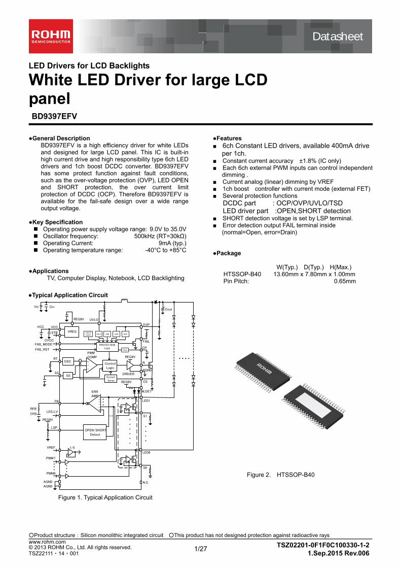
Datasheet ○Product structure:Silicon monolithic integrated circuit ○This product has not designed protection against radioactive rays . 1/27 TSZ02201-0F1F0C100330-1-2 © 2013 ROHM Co., Ltd. All rights reserved. 1.Sep.2015 Rev.006 TSZ22111・14・001 www.rohm.com LED Drivers for LCD Backlights White LED Driver for large LCD panel BD9397EFV ●General Description BD9397EFV is a high efficiency driver for white LEDs and designed for large LCD panel. This IC is built-in high current drive and high responsibility type 6ch LED drivers and 1ch boost DCDC converter. BD9397EFV has some protect function against fault conditions, such as the over-voltage protection (OVP), LED OPEN and SHORT protection, the over current limit protection of DCDC (OCP). Therefore BD9397EFV is available for the fail-safe design over a wide range output voltage. ●Key Specification Operating power supply voltage range: 9.0V to 35.0V Oscillator frequency: 500kHz (RT=30kΩ) Operating Current: 9mA (typ.) Operating temperature range: -40°C to +85°C ●Applications TV, Computer Display, Notebook, LCD Backlighting ●Features ■ 6ch Constant LED drivers, available 400mA drive per 1ch. ■ Constant current accuracy ±1.8% (IC only) ■ Each 6ch external PWM inputs can control independent dimming . ■ Current analog (linear) dimming by VREF ■ 1ch boost controller with current mode (external FET) ■ Several protection functions DCDC part : OCP/OVP/UVLO/TSD LED driver part :OPEN,SHORT detection ■ SHORT detection voltage is set by LSP terminal. ■ Error detection output FAIL terminal inside (normal=Open, error=Drain) ●Package W(Typ.) D(Typ.) H(Max.) HTSSOP-B40 13.60mm x 7.80mm x 1.00mm Pin Pitch: 0.65mm ●Typical Application Circuit Figure 1. Typical Application Circuit Figure 2. HTSSOP-B40 + - - - - - + - + - OPEN/SHORT Detect ERR AMP Control Logic DRIVER Current Sense SS OSC + + PWM COMP - - VREG PROTECTION Logic + PWM1 VREF LSP FB AGND SS RT STB VCC REG9V UVLO FAIL OVP CP N PGND LED1 S1 CS Vin Cin VCC CVCC RFB CFB Cout REG9V + - LED6 S6 LED_LV REG9V UVLO (VCC) UVLO TSD OVP SCP Filter FAIL_MODE PWM6 AGND N.C. REG9V M_DET FAIL_RST 1/5
Transcript of LED Drivers for LCD Backlights White LED Driver for...
Datasheet
Product structure:Silicon monolithic integrated circuit This product has not designed protection against radioactive rays.
1/27 TSZ02201-0F1F0C100330-1-2© 2013 ROHM Co., Ltd. All rights reserved.
1.Sep.2015 Rev.006TSZ22111・14・001
www.rohm.com
LED Drivers for LCD Backlights
White LED Driver for large LCD panel BD9397EFV
General DescriptionBD9397EFV is a high efficiency driver for white LEDs and designed for large LCD panel. This IC is built-in high current drive and high responsibility type 6ch LED drivers and 1ch boost DCDC converter. BD9397EFV has some protect function against fault conditions, such as the over-voltage protection (OVP), LED OPEN and SHORT protection, the over current limit protection of DCDC (OCP). Therefore BD9397EFV is available for the fail-safe design over a wide range output voltage.
Key Specification Operating power supply voltage range: 9.0V to 35.0V Oscillator frequency: 500kHz (RT=30kΩ) Operating Current: 9mA (typ.) Operating temperature range: -40°C to +85°C
ApplicationsTV, Computer Display, Notebook, LCD Backlighting
Features 6ch Constant LED drivers, available 400mA drive
per 1ch. Constant current accuracy ±1.8% (IC only) Each 6ch external PWM inputs can control independent
dimming . Current analog (linear) dimming by VREF 1ch boost controller with current mode (external FET) Several protection functions
DCDC part : OCP/OVP/UVLO/TSDLED driver part :OPEN,SHORT detection
SHORT detection voltage is set by LSP terminal. Error detection output FAIL terminal inside
(normal=Open, error=Drain)
Package
W(Typ.) D(Typ.) H(Max.) HTSSOP-B40 13.60mm x 7.80mm x 1.00mm Pin Pitch: 0.65mm
Typical Application Circuit
Figure 1. Typical Application Circuit
Figure 2. HTSSOP-B40
+
-----
+-
+-
OPEN/SHORT
Detect
ERR AMP
ControlLogic
DRIVERCurrent
Sense
SS
OSC + +
PWM COMP
--
VREG
PROTECTION Logic
+
PWM1
VREF
LSP
FB
AGND
SS
RT
STB
VCC
REG9V UVLO
FAIL
OVP
CP
N
PGND
LED1
S1
CS
Vin Cin
VCC
CVCC
RFB
CFB
Cout
REG9V
+-
LED6
S6
LED_LV
REG9V
UVLO(VCC) UVLO TSD OVP SCP
Filter
FAIL_MODE
PWM6
AGNDN.C.
REG9V
M_DET
FAIL_RST
1/5

DatasheetDatasheet
2/27 TSZ02201-0F1F0C100330-1-2© 2013 ROHM Co., Ltd. All rights reserved.
1.Sep.2015 Rev.006
www.rohm.com
TSZ22111・15・001
BD9397EFV
Absolute maximum ratings (Ta=25°C) Parameter Symbol Ratings Unit
Operating Temperature Range Ta(opr) -40 to +85 °C
Storage Temperature Range Tstg -55 to +150 °C
Power Dissipation Pd 4.7 *1 W
Thermal resistance between junction and case θjc 7 *2 °C/W
Maximum Junction Temperature Tjmax 150 °C
Maximum LED output current ILED 400 *3 *4 mA *1 In the case of mounting 4 layer glass epoxy base-plate of 70mm×70mm×1.6mm, 37.6mW is reduced at 1°C above Ta=25. *2 In the case of mounting 4 layer glass epoxy base-plate of 70mm×70mm×1.6mm. *3 Wide VF variation of LED increases loss at the driver, which results in rise in package temperature. Therefore, the board needs to be designed
with attention paid to heat radiation. *4 This current value is per 1ch. It needs be used within a range not exceeding Pd.
Operating Ratings (Ta = 25°C)
Parameter Symbol Range Unit
Power supply voltage VCC 9 to 35 V
DC/DC oscillation frequency FCT 100 to 1250 *5 kHz
VREF input voltage VREF 0.2 to 2.5 V
LSP terminal input voltage VLSP 0.8 to 3 V
FB terminal output voltage VFB 0 to 3.3 V
M_DET terminal output voltage VM_DET 0 to REG9V V The operating conditions written above are constants of the IC unit. Be careful enough when setting the constant in the actual set.
External Components Recommended Range
Item Symbol Setting Range Unit
VCC terminal connection capacitance CVCC 1.0 to 10 μF
Soft-start set capacitance SS 0.001 to 1.0 μF
Timer latch set capacitance CP 0.001 to 2.7 μF
Operating frequency set resistance RT 12 to 150 kΩ
REG9V terminal connection capacitance CREG9V 2.2 to 10 μF The values described above are constants for a single IC. Adequate attention must be paid to setting of a constant for an actual set of parts
Pin Configuration Physical Dimension Tape and Marking Diagram
Figure 3.
Figure 4-1. SOP-24
LOT No.
BD9397EFV
Figure 4. HTSSOP-B40
BD
9397EF
V

DatasheetDatasheet
3/27 TSZ02201-0F1F0C100330-1-2© 2013 ROHM Co., Ltd. All rights reserved.
1.Sep.2015 Rev.006
www.rohm.com
TSZ22111・15・001
BD9397EFV
1.1 Electrical Characteristics 1(Unless otherwise specified, Ta=25°C,VCC=24V)
Parameter Symbol Limit
Unit Condition Min. Typ. Max.
【Whole device】
Operating circuit current ICC - 9 16 mA STB=3V,LED1-6=ON, RT=30kΩ
Stand-by circuit current ISTB - 12 20 μA STB=0V
【REG9V block】
REG9V output voltage REG9V 8.9 9.0 9.1 V IO=0mA
Maximum REG9V output current IREG9V 20 - - mA
【Switching block】
N terminal source resistance RONH - 2.5 3.5 Ω ION=-10mA
N terminal sink resistance RONL - 3.0 4.2 Ω ION=10mA
【Over current protection (OCP) block】
Over current protection voltage VOCP 0.40 0.45 0.50 V VCS=SWEEP UP
【Soft-start block】
SS terminal source current ISS -1.4 -1.0 -0.6 μA
SS terminal release voltage VSS 2.9 3.0 3.1 V SS=SWEEP UP
【Error amplifier block】
LED control voltage VLED 0.66 0.7 0.74 V LED_LV=0.7V
FB sink current IFBSINK 55 100 155 μA LED=2.0V, VFB=1.0V
FB source current IFBSOURCE -155 -100 -55 μA LED=0V, VFB=1.0V
LED_LV terminal input current ILED_LV -2 0 2 uA VLED_LV=3V
【CT oscillator block】
Oscillation frequency FCT 440 500 560 kHz RT=30kΩ
MAX DUTY DMAX 78 84 91 %
【Over voltage protection (OVP) block】
OVP detection voltage VOVP 2.34 2.43 2.52 V VOVP=SWEEP UP
OVP hysteresis voltage VOVPHYS 10 50 100 mV VOVP=SWEEP DOWN
OVP feedback voltage FBOVP 0.93 1.05 1.17 V PMW1-6=0V,SS=2.8V, VLED_LV=0.7V
【Short current protection (SCP) block】
Short circuit protection voltage VSCPmL 0.12 0.20 0.28 V
VOVP=SWEEP DOWN, FAILMODE=0V
VSCPmH 0.74 0.79 0.84 V VOVP=SWEEP DOWN, FAILMODE=3V
【M_LED block】
Diode forward voltage VFLED 1120 1340 1560 mV VLED=0V
Forward voltage offset each ch VFOFFSET - - 20 mV VLED=0V
REG9V pull up resistance RM_DET 60 100 140 kΩ

DatasheetDatasheet
4/27 TSZ02201-0F1F0C100330-1-2© 2013 ROHM Co., Ltd. All rights reserved.
1.Sep.2015 Rev.006
www.rohm.com
TSZ22111・15・001
BD9397EFV
1.2 Electrical Characteristics 2(Unless otherwise specified, Ta=25°C,VCC=24V)
Parameter Symbol Limit
Unit Condition Min. Typ. Max.
【UVLO block】
Operation power source voltage (VCC) VUVLO_VCC 7.0 7.5 8.0 V VCC=SWEEP UP
Hysteresis voltage (VCC) VUHYS_VCC 150 300 600 mV VCC=SWEEP DOWN
UVLO Release voltage VUVLO_U 2.375 2.5 2.625 V VUVLO=SWEEP UP
Hysteresis voltage (UVLO) VUHYS_U 50 100 150 mV VUVLO=SWEEP DOWN
UVLO terminal input resistance RUVLO 370 610 850 kΩ VUVLO=3V
【Filter block】
CP detection voltage VCP 1.9 2.0 2.1 V CP=SWEEP UP
CP source current ICP -1.2 -1.0 -0.8 μA VCP=0V
【LED driver block】
S terminal voltage VSLED
196 200 204 mV VREF=1.0V
294.6 300 305.4 mV VREF=1.5V
392.8 400 407.2 mV VREF=2.0V
491 500 509 mV VREF=2.5V
LED current rise time ILEDtr - 400 760 ns VREF=0.3V,RS=2Ω
LED current fall time ILEDtf - 100 280 ns VREF=0.3V,RS=2Ω
OPEN detection voltage VOPEN 0.12 0.20 0.28 V VLED=SWEEP DOWN
SHORT detection voltage VSHORT 5.7 6.0 6.3 V VLED=SWEEPUP, VLSP=1.2V
SHORT MASK voltage VSHTMASK 2.85 3.0 3.15 V
VREF terminal input current IVREF -2 0 2 μA VVREF=3V
LSP terminal input current ILSP -2 0 2 μA VLSP=3V
【STB block】
STB terminal HIGH voltage STBH 2.0 - VCC V
STB terminal LOW voltage STBL -0.3 - 0.8 V
STB terminal Pull Down resistance RSTB 0.5 1.0 1.5 MΩ STB=3V
【PWM IN block】
PWM terminal HIGH voltage PWMH 2.0 - 20 V
PWM terminal LOW voltage PWML -0.3 - 0.8 V
PWM terminal Pull Down resistance RPWM 200 300 400 kΩ PWM=3V
【FAIL_MODE,FAIL_RST,SUMPWM block】
Input terminal High voltage VINH 2.0 - 20 V
Input terminal Low voltage VINL -0.3 - 0.8 V
Input terminal Pull Down resistance RVIN 60 100 140 kΩ VIN=3V
【FAIL block(OPEN DRAIN)】
FAIL LOW output voltage VOL 0.25 0.5 1.0 V IOL=1mA

DatasheetDatasheet
5/27 TSZ02201-0F1F0C100330-1-2© 2013 ROHM Co., Ltd. All rights reserved.
1.Sep.2015 Rev.006
www.rohm.com
TSZ22111・15・001
BD9397EFV
1.3 Pin Descriptions
No Pin name In/Out Function rating
[V]
1 VCC IN Power source terminal -0.3 to 36
2 FAIL OUT Abnormality detection output terminal (OPEN DRAIN) -0.3 to 36
3 REG9V OUT 9V regulator output terminal -0.3 to 13
4 N.C. - Non connection terminal -
5 N OUT DC/DC switching output terminal -0.3 to 13
6 PGND IN Power GND terminal -
7 CS IN DC/DC FET output current detection terminal -0.3 to 7
8 OVP IN Overvoltage protection detection terminal -0.3 to 7
9 M_DET OUT LED Diode OR output terminal -0.3 to 13
10 AGND IN GND terminal for analog part -
11 LED1 OUT LED output 1 -0.3 to 50
12 LED2 OUT LED output 2 -0.3 to 50
13 LED3 OUT LED output 3 -0.3 to 50
14 LED4 OUT LED output 4 -0.3 to 50
15 LED5 OUT LED output 5 -0.3 to 50
16 LED6 OUT LED output 6 -0.3 to 50
17 STB IN Standby control terminal -0.3 to 36
18 PWM1 IN PWM dimming input signal terminal for LED 1 -0.3 to 22
19 PWM2 IN PWM dimming input signal terminal for LED 2 -0.3 to 22
20 PWM3 IN PWM dimming input signal terminal for LED 3 -0.3 to 22
21 PWM4 IN PWM dimming input signal terminal for LED 4 -0.3 to 22
22 PWM5 IN PWM dimming input signal terminal for LED 5 -0.3 to 22
23 PWM6 IN PWM dimming input signal terminal for LED 6 -0.3 to 22
24 FAIL_RST IN FAIL output reset terminal -0.3 to 22
25 S6 IN Connecting terminal for LED 6 constant current setting resistor -0.3 to 7
26 S5 IN Connecting terminal for LED 5 constant current setting resistor -0.3 to 7
27 S4 IN Connecting terminal for LED 4 constant current setting resistor -0.3 to 7
28 S3 IN Connecting terminal for LED 3 constant current setting resistor -0.3 to 7
29 S2 IN Connecting terminal for LED 2 constant current setting resistor -0.3 to 7
30 S1 IN Connecting terminal for LED 1 constant current setting resistor -0.3 to 7
31 CP OUT Connecting terminal for non-reaction time setting capacitor -0.3 to 7
32 SS OUT Connecting terminal for soft-start time setting capacitor -0.3 to 7
33 FB OUT Error amplifier output terminal -0.3 to 7
34 RT OUT Connecting terminal for DC/DC frequency setting resistor -0.3 to 7
35 VREF IN Analog dimming DC voltage input terminal -0.3 to 7
36 LED_LV IN LED control voltage set terminal -0.3 to 7
37 LSP IN LED SHORT detection voltage setting terminal -0.3 to 7
38 FAIL_MODE IN FAIL function change terminal -0.3 to 7
39 UVLO IN Low voltage malfunction prevention detection terminal -0.3 to 10.5
40 AGND IN GND terminal for analog part -
DatasheetDatasheet
6/27 TSZ02201-0F1F0C100330-1-2© 2013 ROHM Co., Ltd. All rights reserved.
1.Sep.2015 Rev.006
www.rohm.com
TSZ22111・15・001
BD9397EFV
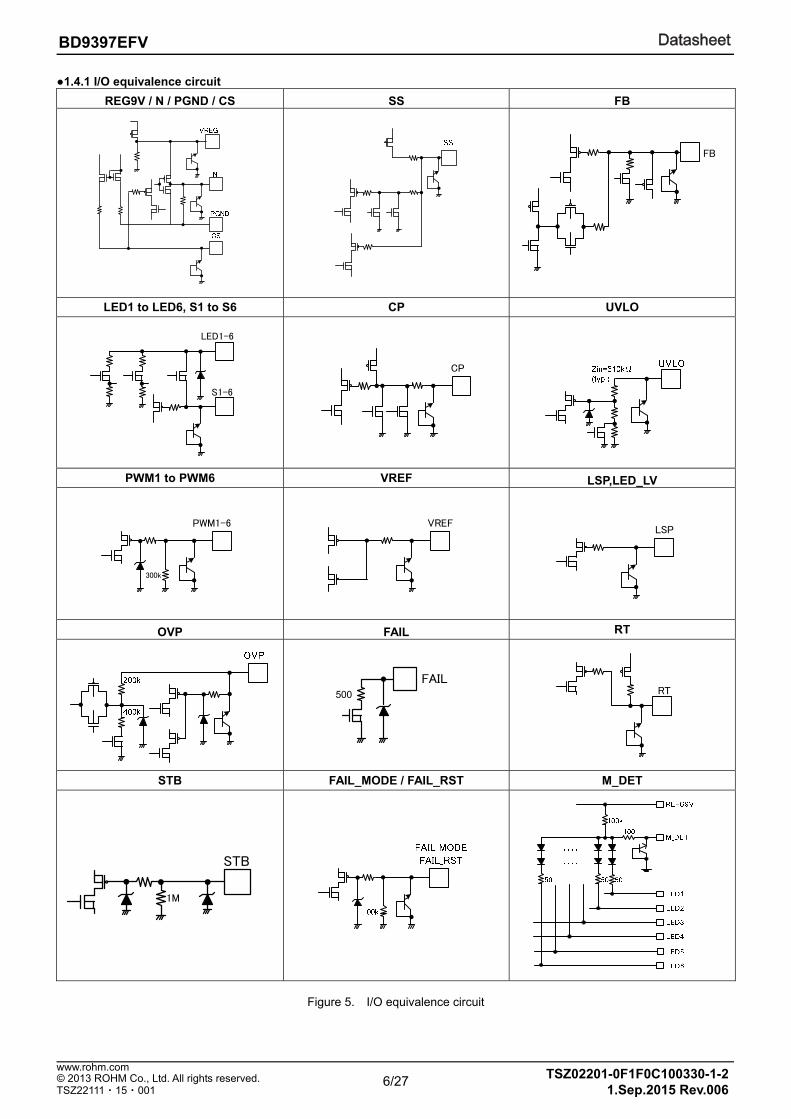
1.4.1 I/O equivalence circuit
REG9V / N / PGND / CS SS FB
FB
LED1 to LED6, S1 to S6 CP UVLO
LED1-6
S1-6
CP
PWM1 to PWM6 VREF LSP,LED_LV
PWM1-6
300k
VREF
LSP
OVP FAIL RT
FAIL500
RT
STB FAIL_MODE / FAIL_RST M_DET
STB
1M
Figure 5. I/O equivalence circuit

DatasheetDatasheet
7/27 TSZ02201-0F1F0C100330-1-2© 2013 ROHM Co., Ltd. All rights reserved.
1.Sep.2015 Rev.006
www.rohm.com
TSZ22111・15・001
BD9397EFV
1.5Typical Performance Curves(reference data)
0
10
20
30
40
50
10 14 18 22 26 30 34VCC [V]
Istb
[uA
]
0
2
4
6
8
10
12
14
10 14 18 22 26 30 34VCC [V]
Icc
[mA
]
Figure 7. Stand-by circuit current
STB=3V
PWM1-6=0V
Ta=25°C
Figure 6. Circuit current
0
30
60
0 1 2 3PWM1 [V]
ILED
1 [
mA
]
VCC=24V
RS=20Ω
Ta=25°C
Figure 9. VREF v.s. Sx
Figure 10. PWM terminal threshold voltage
STB=0V
PWM1-6=0V
Ta=25°C
0
200
400
600
800
1000
0 1 2 3 4VREF [V]
S1
[mV
]
VCC=24V
RS=2Ω
LED1=2.5V
Ta=25°C
0
20
40
60
80
100
0 1 2 3 4FB [V]
Duty
Cyc
le [
%]
VCC=24V
Ta=25°C
Figure 8. FB v.s. Duty Cycle
DatasheetDatasheet
8/27 TSZ02201-0F1F0C100330-1-2© 2013 ROHM Co., Ltd. All rights reserved.
1.Sep.2015 Rev.006
www.rohm.com
TSZ22111・15・001
BD9397EFV
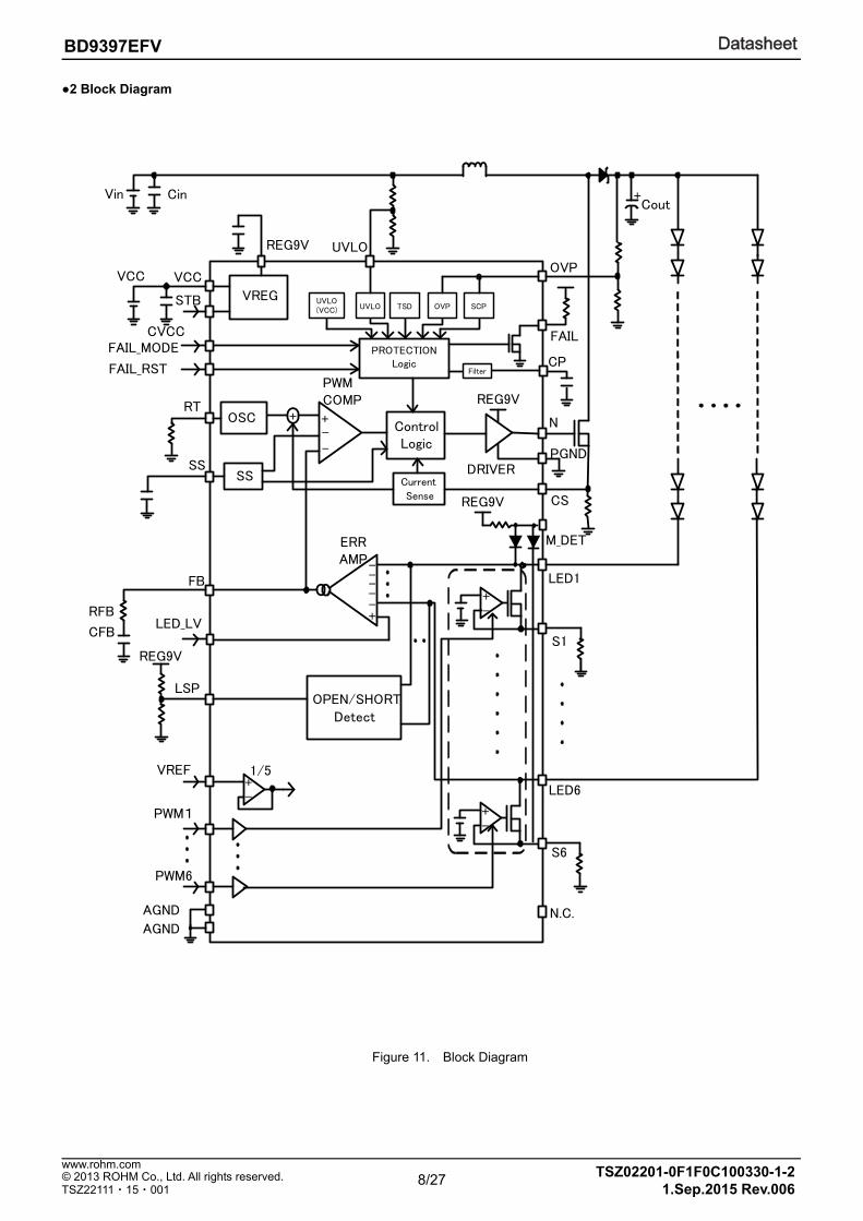
2 Block Diagram
+
-----
+-
+-
OPEN/SHORTDetect
ERR AMP
ControlLogic
DRIVERCurrent
Sense
SS
OSC + +
PWM COMP
--
VREG
PROTECTION Logic
+
PWM1
VREF
LSP
FB
AGND
SS
RT
STB
VCC
REG9V UVLO
FAIL
OVP
CP
N
PGND
LED1
S1
CS
Vin Cin
VCC
CVCC
RFB
CFB
Cout
REG9V
+-
LED6
S6
LED_LV
REG9V
UVLO(VCC) UVLO TSD OVP SCP
Filter
FAIL_MODE
PWM6
AGNDN.C.
REG9V
M_DET
FAIL_RST
1/5
Figure 11. Block Diagram
DatasheetDatasheet
9/27 TSZ02201-0F1F0C100330-1-2© 2013 ROHM Co., Ltd. All rights reserved.
1.Sep.2015 Rev.006
www.rohm.com
TSZ22111・15・001
BD9397EFV
3.1 Pin Configuration 1 pin. VCC
Power supply terminal of IC. The input range is 9 to 35V. The operation starts over VCC=7.5V(typ.) and the system stops under VCC=7.2V(typ.).
2 pin. FAIL
FAIL signal output terminal (NMOS open-drain). NMOS is OPEN at the normal operation so FAIL pin is Hi-Z. NMOS becomes ON state (500 ohm typ.) at the abnormal detection. It is possible to select the FAIL type from latch type (FAIL_MODE=L) or one shot pulse (FAIL_MODE=H).Please refer to the detail explanation<38pin. FAIL_MODE terminal>
3 pin. REG9V
REG9V is a 9 V output pin used delivering 20mA at maximum for switching power supply of N terminal. Use at a current higher than 20mA may affect the reference voltage within IC, which may result in malfunction. It will also cause heating of IC itself. Therefore it is recommended to set the load as small as possible. The characteristic of VCC line regulation at REG9V is shown as figure. VCC must be used in more than 10.5V for stable 9V output. Install an oscillation prevention ceramic capacitor (2.2 to 10μF) nearest to VREG between VREG-AGND terminals.
4 pin. N.C
Non connect pin. Please set it the open state or deal with connecting the GND. 5 pin. N
Gate driving output pin of external NMOS of DC/DC converter with 0 to 9V (REG9V) swing. Output resistance of High side is 2.5 ohm(typ.), Low side is 3.0 ohm(typ.) in ON state. The oscillation frequency is set by a resistance connected to RT pin. For details, see the explanation of <34pin. RT terminal>.
6pin. PGND
Power GND terminal of output terminal, N driver: 7pin. CS
Inductor current detection resistor connecting terminal of DC/DC current mode: it transforms the current flowing through the inductor into voltage by sense resistor RCS connected to CS terminal, and this voltage is compared with that set in the error amplifier by current detection comparator to control DC/DC output voltage. RCS also performs over current protection (OCP) and stops switching action when the voltage of CS terminal is 0.45 V (typ.) or higher (Pulse by Pulse).
8 pin. OVP
OVP terminal is the detection terminal of overvoltage protection (OVP) and short circuit protection (SCP) for DC/DC output voltage. Depending on the setting of the FAIL_MODE terminal, FAIL and CP terminal behave differently when an abnormality is detected. For details, see the table for each protection operation is described in 3.2 and 3.3. During the soft start (SS), there is a function which returns the OVP voltage to error amplifier to boost DC/DC output voltage at all Low PWM (OVPFB function). After completion of SS, this function is disabled.
9 pin. M_DET
The Di OR output terminal of LED 1 to 6. The output is the voltage which is added a diode forward voltage(two diode stack) to the lowest voltage among 6 LED terminals.
10pin. AGND
Analog GND for IC
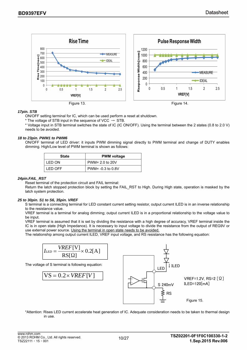
11 to 16pin. LED1 to LED6 LED constant current driver output terminal. Setting of LED current value is adjustable by setting the VREF voltage and connecting a resistor to S terminal. For details, see the explanation of <25 to 30pin. S1 to S6, 35pin. VREF >. The PWM dimming frequency of LED current driver and upper/lower limit of the duty need to be set in a manner that necessary linearity of PWM dimming characteristics can be secured referring to the following figures: Start/Stop time of constant current driver (PWM pulse response) Start-up time depends on the VREF value; the response becomes quick, so that voltage is high. In the way of reference, the current response upon application of current rise rate and pulse PWM1us (current pulse) to describe the dependence of VREF. It needs to be adequately verified with an actual device because the response rate may vary with application conditions.
Figure 12.
‐1
0
1
2
3
4
5
6
7
8
9
10
0 5 10 15 20 25 30 35
REG
9V [V]
VCC [V]
REG9V ‐VCC (Line Regulation)
DatasheetDatasheet
10/27 TSZ02201-0F1F0C100330-1-2© 2013 ROHM Co., Ltd. All rights reserved.
1.Sep.2015 Rev.006
www.rohm.com
TSZ22111・15・001
BD9397EFV
17pin. STB
ON/OFF setting terminal for IC, which can be used perform a reset at shutdown. * The voltage of STB input in the sequence of VCC → STB. * Voltage input in STB terminal switches the state of IC (IC ON/OFF). Using the terminal between the 2 states (0.8 to 2.0 V) needs to be avoided.
18 to 23pin. PWM1 to PWM6
ON/OFF terminal of LED driver: it inputs PWM dimming signal directly to PWM terminal and change of DUTY enables dimming. High/Low level of PWM terminal is shown as follows:
State PWM voltage
LED ON PWM= 2.0 to 20V
LED OFF PWM= -0.3 to 0.8V
24pin.FAIL_RST
Reset terminal of the protection circuit and FAIL terminal: Return the latch stopped protection block by setting the FAIL_RST to High. During High state, operation is masked by the latch system protection.
25 to 30pin. S1 to S6, 35pin. VREF
S terminal is a connecting terminal for LED constant current setting resistor, output current ILED is in an inverse relationship to the resistance value. VREF terminal is a terminal for analog dimming; output current ILED is in a proportional relationship to the voltage value to be input. VREF terminal is assumed that it is set by dividing the resistance with a high degree of accuracy, VREF terminal inside the IC is in open state (High Impedance). It is necessary to input voltage to divide the resistance from the output of REG9V or use external power source. Using the terminal in open state needs to be avoided. The relationship among output current ILED, VREF input voltage, and RS resistance has the following equation:
The voltage of S terminal is following equation: *Attention: Rises LED current accelerate heat generation of IC. Adequate consideration needs to be taken to thermal design
in use.
LED
+
-
↓ILED
RS
S 240mV
VREF=1.2V, RS=2 [Ω]ILED=120[mA]
Ω
]A[0.2]RS[
[V]
VREFILED
][2.0VS VVREF
Figure 13. Figure 14.
Figure 15.
0
200
400
600
800
1000
1200
0 0.5 1 1.5 2 2.5
Rsep
on
se W
idth
[nsec]
VREF[V]
Pulse Response Width
MEASURE
IDEAL0
100200300400500600700800
0 0.5 1 1.5 2 2.5
Ris
e T
ime
[ns
ec
]
VREF[V]
Rise Time
MEASURE
IDEAL

DatasheetDatasheet
11/27 TSZ02201-0F1F0C100330-1-2© 2013 ROHM Co., Ltd. All rights reserved.
1.Sep.2015 Rev.006
www.rohm.com
TSZ22111・15・001
BD9397EFV
0
0.2
0.4
0.6
0.8
1
1.2
0 50 100 150 200 250 300 350 400
Nee
ded
LED
-S V
olta
ge
LED Current Setting
Voltage between LEDx to Sx vs LED Current (Tj=25, 85deg.)
85 25
* For the adjustment of LED current with analog dimming by VREF, note that the output voltage of the DC/DC converter largely changes accompanied by LED VF changes if the VREF voltage is changed rapidly. In particularly, when the VREF voltages become high to low, it makes the LED terminal voltage seem higher transiently, which may influence application such as activation of the LED short circuit protection. It needs to be adequately verified with an actual device when analog dimming is used.
31pin. CP
Terminal which sets the time from detection of abnormality until shutdown (Timer latch). When the LED short protection, LED open protection or SCP is detected, it perform s constant current charge of 1.0uA (typ.) to external capacitor. When the CP terminal voltage reaches 2.0V (typ.), the IC is latched and FAIL terminal operates (at FAIL_MODE = L).
32pin. SS
Terminal which sets soft-start time of DC/DC converter: it performs constant current charge of 1.0uA to the external capacitor connected with SS terminal, which enables soft-start of DC/DC converter. Since the LED protection function (OPEN/SHORT detection) works when the SS terminal voltage reaches 3.0 V (typ.) or higher, it must be set to bring stability to conditions such as DC/DC output voltage and LED constant current drive operation, etc. before the voltage of 3.0 V is detected.
33pin. FB
Output terminal of the error amplifier of DC/DC converter which controls current mode: The voltage of LED terminal which is the highest VF voltage among 6 LED strings and the voltage of LED_LV terminal become input of the error amplifier. The DC/DC output voltage is kept constant to control the duty of the output N terminal by adjusting the FB voltage. The voltage of other LED terminals is, as a result, higher by the variation of Vf. Phase compensation setting is separately described in 3.7 How to set phase compensation. A resistor and a capacitor need to be connected in series nearest to the terminal between FB and AGND. The state in which all PWM signals are in LOW state brings high Impedance, keeping FB voltage. This action removes the time of charge to the specified voltage, which results in speed-up in DC/DC conversion.
34pin. RT RT sets charge/discharge current determining frequency inside IC. Only a resistor connected to RT determines the drive frequency inside IC, the relationship has the following equation: FCT is 500 kHz at RT= 30 kohm.
36pin. LED_LV
LED_LV terminal sets the reference voltage error amplifier. LED_LV terminal is assumed that it is set by dividing the resistance with a high degree of accuracy, LED_LV terminal inside the IC is in open state (High Impedance). It is necessary to input voltage to divide the resistance from the output of REG9V or use external power source. Using the terminal in open state needs to be avoided. According to output current, lowering LED_LV voltage can reduce the loss and heat generation inside IC. However, it is necessary to ensure the voltage between drain and source of FET inside IC, so LED_LV voltage has restriction on the following equation.
VLED_LV ≧ (LED-S terminal voltage) + 0.2×VREF [V] For example, at ILED = 100mA setting by VREF = 1V, from figure the voltage between LED and S terminal is required 0.27 V at Tj = 85°C, so LED_LV voltage must be at least a minimum 0.47V.
Note: Rises in VLED_LV voltage and LED current accelerate heat generation of IC. Adequate consideration needs to be taken to thermal design in use.
Note: LED_LV voltage is not allowed setting below 0.3V. Note: LED current by raising LED_LV voltage can flow to MAX 400mA, use with care in the dissipation of the package.
Figure 16. Figure 17.
10
100
1000
10000
1 10 100 1000
FCT [kHz]
RT [kOhm]
FCT vs RT(measurement data)

DatasheetDatasheet
12/27 TSZ02201-0F1F0C100330-1-2© 2013 ROHM Co., Ltd. All rights reserved.
1.Sep.2015 Rev.006
www.rohm.com
TSZ22111・15・001
BD9397EFV
LED_LV
LED1
LED2
S1
-
+
S2
S3
S4
S5
S6
-
+
-
+
-
+
-
+
-
+
LED3
LED4
LED5
LED6
REG9V
AMP
+
--
---
-
37pin. LSP Terminal which sets LED SHORT detection voltage: The input impedance of LSP pin is High Impedance, because it is assumed that the input of LSP terminal is set by dividing the resistance with a high degree of accuracy. The LSP terminal is assumed that it is set by dividing the resistance with a high degree of accuracy, LSP terminal inside the IC is in open state (High Impedance). It is necessary to input voltage to divide the resistance from the output of REG9V or use external power source. Using the terminal in open state needs to be avoided. Set LSP voltage in the range of 0.8V to 3.0V.
LEDSHORT:LSP detection Voltage, VLSP:LSP terminal voltage The conditions there are restrictions on short LED detection. For details, see the explanation of section 3.5.2 Setting the LED short detect voltage (LSP pin).
. 38pin. FAIL_MODE
Output mode of FAIL can be change by FAIL_MODE terminal. When FAIL_MODE is in Low state, the output of FAIL terminal is the latch mode. FAIL terminal is latched after the CP charge time from detection of abnormal state. When FAIL_MODE is in High state, the output of FAIL terminal is one-shot-pulse mode. At detected abnormality, firstly FAIL is in Low state (Drain state). FAIL returns to High state (Open state) if abnormality is cleared after CP charge time, In this mode, there is no latch stop for protection operation in IC. Monitoring the FAIL with the Microcomputer, decide to stop working IC. For FAIL_MODE = H when the detection sequence, see the explanation of section 3.8.3 Protective operation sequence at FAIL_MODE=H. On application to change modes is prohibited.
39pin. UVLO
UVLO terminal of the power of step-up DC/DC converter: at 2.5 V (typ.) or higher, IC starts step-up operation and stops at 2.4V or lower (typ.). (It is not shutdown of IC.) UVLO can be used to perform a reset after latch stop of the protections. The power of step-up DC/DC converter needs to be set detection level by dividing the resistance. If any problem on the application causes noise on UVLO terminal which results in unstable operation of DC/DC converter, a capacitance of approximately 1000 pF needs to be connected between UVLO and AGND terminals.
40pin. AGND
Analog GND for IC
][5 VVLSPLED SHORT
Figure 18.
DatasheetDatasheet
13/27 TSZ02201-0F1F0C100330-1-2© 2013 ROHM Co., Ltd. All rights reserved.
1.Sep.2015 Rev.006
www.rohm.com
TSZ22111・15・001
BD9397EFV
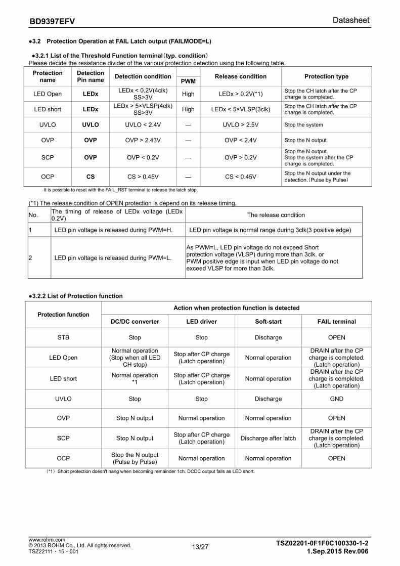
3.2 Protection Operation at FAIL Latch output (FAILMODE=L) 3.2.1 List of the Threshold Function terminal(typ. condition)
Please decide the resistance divider of the various protection detection using the following table.
Protection name
Detection Pin name
Detection condition
Release condition Protection type PWM
LED Open LEDx LEDx < 0.2V(4clk)
SS>3V High LEDx > 0.2V(*1) Stop the CH latch after the CP
charge is completed.
LED short LEDx LEDx > 5×VLSP(4clk)
SS>3V High LEDx < 5×VLSP(3clk) Stop the CH latch after the CP
charge is completed.
UVLO UVLO UVLO < 2.4V ― UVLO > 2.5V Stop the system
OVP OVP OVP > 2.43V ― OVP < 2.4V Stop the N output
SCP OVP OVP < 0.2V ― OVP > 0.2V Stop the N output. Stop the system after the CP charge is completed.
OCP CS CS > 0.45V ― CS < 0.45V Stop the N output under the detection.(Pulse by Pulse)
It is possible to reset with the FAIL_RST terminal to release the latch stop.
(*1) The release condition of OPEN protection is depend on its release timing.
No. The timing of release of LEDx voltage (LEDx 0.2V)
The release condition
1 LED pin voltage is released during PWM=H. LED pin voltage is normal range during 3clk(3 positive edge)
2 LED pin voltage is released during PWM=L.
As PWM=L, LED pin voltage do not exceed Short protection voltage (VLSP) during more than 3clk. or PWM positive edge is input when LED pin voltage do not exceed VLSP for more than 3clk.
3.2.2 List of Protection function
(*1)Short protection doesn't hang when becoming remainder 1ch. DCDC output falls as LED short.
Protection function Action when protection function is detected
DC/DC converter LED driver Soft-start FAIL terminal
STB Stop Stop Discharge OPEN
LED Open Normal operation
(Stop when all LED CH stop)
Stop after CP charge (Latch operation)
Normal operation DRAIN after the CP charge is completed.
(Latch operation)
LED short Normal operation
*1 Stop after CP charge
(Latch operation) Normal operation
DRAIN after the CP charge is completed.
(Latch operation)
UVLO Stop Stop Discharge GND
OVP Stop N output Normal operation Normal operation OPEN
SCP Stop N output Stop after CP charge
(Latch operation) Discharge after latch
DRAIN after the CP charge is completed.
(Latch operation)
OCP Stop the N output (Pulse by Pulse)
Normal operation Normal operation OPEN

DatasheetDatasheet
14/27 TSZ02201-0F1F0C100330-1-2© 2013 ROHM Co., Ltd. All rights reserved.
1.Sep.2015 Rev.006
www.rohm.com
TSZ22111・15・001
BD9397EFV
3.3 Protection operation when the FAIL one shot outputs(FAILMODE=H) 3.3.1 List of the threshold function terminal (typ. condition)
Please decide the resistance divider of the various protection detection using the following table.
Protection name
Detection Pin name
Detection condition
Release condition Protection type
PWM
LED Open LEDx LEDx < 0.2V(4clk)
SS>3V High LEDx > 0.2V(3clk)
FAIL drain state under the detection.
LED short LEDx LEDx > 5×VLSP(4clk)
SS>3V High LEDx < 5×VLSP(3clk)
FAIL drain state under the detection.
UVLO UVLO UVLO < 2.4V ― UVLO > 2.5V Stop the system.
OVP OVP OVP > 2.43V ― OVP < 2.4V Stop the system FAIL drain state under the detection..
SCP OVP OVP < 0.79V ― OVP > 0.79V Stop the system. FAIL drain state under the detection..
OCP CS CS > 0.45V ― CS < 0.45V Stop the N output under the detection. (Pulse by Pulse)
3.3.2 List of the protection function
Protection function
Action when protection function is detected
DC/DC converter LED driver Soft-start FAIL terminal
STB Stop Stop Discharge OPEN
LED Open Normal operation
(Stop when the all CH stop)
Normal operation Normal operation DRAIN under the detection
LED short Normal operation Normal operation Normal operation DRAIN under the detection
UVLO Stop Stop Discharge DRAIN
OVP Stop the N output Normal operation Normal operation DRAIN
SCP Stop the N output Normal operation Normal operation DRAIN
OCP Stop the N output (Pulse by Pulse)
Normal operation Normal operation OPEN

DatasheetDatasheet
15/27 TSZ02201-0F1F0C100330-1-2© 2013 ROHM Co., Ltd. All rights reserved.
1.Sep.2015 Rev.006
www.rohm.com
TSZ22111・15・001
BD9397EFV
5][
][][
AI
VVohmR
LED
VREFS
]V[0.3
]A[100.1]S[T]F[C
6SS
SS
]V[0.2
]A[100.1]S[T]F[C
6CP
CP
+
-
LSP
CLSP
REG9V=9V
R1
R2
LEDx3200kΩ
800kΩ
LSP COMP
3.4 Setting of the external components.(typ. condition) 3.4.1 Setting the LED current (VREF and Sx pin)
First, VREF pin voltage is determined. When performing Analog dimming, be careful of VREF pin input range (0.2 to 2.5V) and decide typical voltage. In BD9397EFV, LED constant current is controlled by Sx terminal voltage as a reference point. Sx terminal is controlled to become one fifth of the voltage of VREF terminal voltage. In the case of VREF=1V, it is set to Sx=0.2V. Therefore, when the resistance to Sx terminal versus GND is set to "RS", the relationship between RS, VREF and ILED is as follows
3.4.2 Setting the LED short detect voltage (LSP pin)
The voltage of LED short detection can be arbitrarily set up with LSP pin voltage. LSP pin cannot be used by OPEN because of High Impedance. Please be sure to applied voltage from the exterior. About LED short detection voltage, if "VLEDshort" and LSP pin voltage are set to "VLSP", it is as follows. Since the setting range of a LSP pin is set to 0.8V to 3.0V, VLEDshort can be set up in 4Vto15V.
Equation of setting LSP detect Voltage When the detection voltage VLSP of LSP is set up by resistance division of R1 and R2 using REG9V, it becomes like the following formula.
*Also including the variation in IC, please also take the part variation in a set into consideration for an actual constant setup, and inquire enough to it.
3.4.3 Timer latch time(CP pin)
When various abnormalities are detected, the source current of 1.0uA is first flowed from CP pin. BD9397EFV don’t stop by latch, unless abnormal state is continues and CP pin voltage reaches continues 2V. With the capacity linked to CP pin, the unresponded time from detection to a latch stop. The relationship between the unresponded time “Tcp” and CP pin connection capacitor “Ccp” is as follows.
3.4.4 Setting the soft-start time (SS pin)
The starting time of a DCDC output is dependent on SS pin connection capacity. Moreover, although SS pin is charged by source current of 1uA, IC does not perform LED protection as under DCDC starting state until SS pin voltage arrive to 3.0V. (The soft starting time set up here should be the mask time of a under [ starting ], and please keep in mind that it differs from time until a DCDC output is stabilized.) Time until a DCDC output is stabilized is greatly dependent on a ratio of step-up or load. The relationship between soft starting time "TSS" and SS pin connection capacity "CSS" is as follows.
3.4.5 DCDC operation frequency (RT pin)
The oscillation frequency of the DCDC output is decided by RT resistance. BD9397EFV is designed to become a 500-kHz setup at the time of 30kohm. RT resistance and frequency have a relation of an inverse proportion, and become settled as the following formula.
=DCDC convertor oscillation frequency [Hz]
Please connect RT resistance close as much as possible from RT pin and an AGND pin.
][105.1 10
SW
RT fR swf
5
][][
VVLEDVV short
LSP
][521
29 V
RR
RVREGVLEDshort
Figure 19.

DatasheetDatasheet
16/27 TSZ02201-0F1F0C100330-1-2© 2013 ROHM Co., Ltd. All rights reserved.
1.Sep.2015 Rev.006
www.rohm.com
TSZ22111・15・001
BD9397EFV
3.4.6 Maximum DCDC output voltage(Vout ,Max) The DCDC output maximum voltage is restricted by Max Duty of N output. Moreover, the voltage needed in order that Vf may modulate by LED current also with the same number of LEDs. Vf becomes high, so that there is generally much current. When you have grasped the variation factor of everythings, such as variation in a DCDC input voltage range, the variation and temperature characteristics of LED load, and external parts, please carry out a margin setup.
3.4.7 Setting the OVP
In BD9397EFV, when over voltage in VOUT line is detected, the instant stop of the N pin output is carried out, and voltage rise operation is stopped. But the latch stop by CP charge is not performed. If VOUT drops by naturally discharge, it is less than the hysteresis voltage of OVP detection and the oscillation condition is fulfilled, N output will be resumed again.
Equation of setting OVP detect
N pin output is suspended at the time of SCP detection, it stops step-up operation, and the latch protection by CP timer.
Equation of setting SCP detect
Moreover, there is an OVPFB function which returns OVP voltage and controls error amplifier so that output voltage may be raised, even when there is no PWM signal during a soft start.
The VOUT setting formula by OVPFB in Soft Start
3.4.8 FAIL Logic
FAIL signal output pin (OPEN DRAIN); when an abnormality is detected, NMOS is brought into GND Level. The rating of this pin is 36V.
State FAIL output
In normal state, In STB OPEN
In completion of an abnormality, when the UVLO is detected(after CP latch)
GND Level (500ohm typ.)
3.4.9 How to set the UVLO
UVLO pin detect the power supply voltage: Vin for step-up DC/DC converters. Operation starts operation on more than 2.5V (typ.) and Operation stops on less than 2.4V (typ.) . Since internal impedance exists in UVLO pin, cautions are needed for selection of resistance for resistance division. A Vin voltage level to make it detecting becomes settled like the following formula by resistance division of R1 and R2 (unit: kΩ). Equation of setting UVLO release Equation of setting UVLO lock
*Also including the variation in IC, please also take the part variation in a set into consideration for an actual constant setup, and inquire enough to it.
][1480530
1
1251400
1
2
215.2 VR
kkkkR
RRVinDET
UVLO
1000pF
AGND AGND
Vin
R2
ΩZin=610k(typ.)
530k
480k
1400k
125k
R1
][140480530
1
1251400
1
2
214.2 VR
kkkkkR
RRVinlock
][2
2143.2 V
R
RRVOVP
][2
212.0 V
R
RRVSCP
OVP
VOUT
R2
R1
2.43V
+
-
+
-
OVP COMP
SCP COMP
0.2V
+
-ERR AMP
LED_LV
FB
REG9V=9V
200k
400k
][400
1
2
21
2
3_ VV
R
R
RRVOUT LVLED
Figure 21.
Figure 20.

DatasheetDatasheet
17/27 TSZ02201-0F1F0C100330-1-2© 2013 ROHM Co., Ltd. All rights reserved.
1.Sep.2015 Rev.006
www.rohm.com
TSZ22111・15・001
BD9397EFV
3.4.10 Setting of the LED_LV voltage (LED_LV pin) LED_LV pin is in the OPEN (High Impedance) state. Please be sure to use an external seal of approval, carrying out by inputting REG9V output by resistance division. It cannot use in the state of OPEN. Equation of Setting LED_LV voltage When LED_LV voltage is set up by resistance division of R1 and R2 using REG9V, it becomes like the following formula. *Also including the variation in IC, please also take the part variation in a set into consideration for an actual constant setup, and inquire enough to it.
3.5 Selecting of DCDC part Selecting inductor L
The value of inductor has a great influence on input ripple current. As shown in Equation (1), as the inductor becomes large and switching frequency becomes high, the ripple current of an inductor ⊿IL becomes low.
(1)][)(
・・・・・ Δ AfVL
VVVIL
SWOUT
ININOUT
When the efficiency is expressed by Equation (2), input peak current will be given by Equation (3).
(2) ・・・・・ININ
OUTOUT
IV
IV
(3)22
・・・・・ Δ
Δ IL
V
IVILIIL
IN
OUTOUTINMAX
Here,
L: reactance value [H] VOUT: DC/DC output voltage [V]
VIN: input voltage [V]
LOUT: output load current (total of LED current) [A]
IIN: input current [A] FSW: oscillation frequency [Hz] Generally, ⊿IL is set at around 30 to 50 % of output load current.
* Current exceeding the rated current value of inductor flown through the coil causes magnetic saturation, resulting in decrease in efficiency. Inductor needs to be selected to have such adequate margin that peak current does not exceed the rated current value of the inductor.
* To reduce inductor loss and improve efficiency, inductor with low resistance components (DCR, ACR) needs to be selected.
Selecting output capacitor COUT
Output capacitor needs to be selected in consideration of equivalent series resistance required to even the stable area of output voltage or ripple voltage. Be aware that set LED current may not be flown due to decrease in LED terminal voltage if output ripple voltage is high. Output ripple voltage ⊿VOUT is determined by Equation (4):
(4)][11
・・・・・ Δ Vf
I
CRILMAXV
SW
OUT
OUTESROUT
RESR: equivalent series resistance of COUT
* Rating of capacitor needs to be selected to have adequate margin against output voltage. * To use an electrolytic capacitor, adequate margin against allowable current is also necessary. Be aware that current larger than set value flows transitionally in case that LED is provided with PWM dimming especially.
VOUT
VIN
COUTRCS
LIL
][21
29_ V
RR
RVREGV LVLED
Figure 24.
ΔIL
VOUT
VIN
COUTRCS
L
RESR
IL
Figure 23.
Figure 22.

DatasheetDatasheet
18/27 TSZ02201-0F1F0C100330-1-2© 2013 ROHM Co., Ltd. All rights reserved.
1.Sep.2015 Rev.006
www.rohm.com
TSZ22111・15・001
BD9397EFV
Selecting switching MOSFET Though there is no problem if the absolute maximum rating is the rated current of L or (withstand voltage of COUT + rectifying diode) VF or higher, one with small gate capacitance (injected charge) needs to be selected to achieve high-speed switching. * One with over current protection setting or higher is recommended. * Selection of one with small ON resistance results in high efficiency.
Selecting rectifying diode
A schottky barrier diode which has current ability higher than the rated current of L, reverse voltage larger than withstand voltage of COUT, and low forward voltage VF especially needs to be selected.
Selecting MOSFET for load switch and its soft-start
As a normal step-up DC/DC converter does not have a switch on the path from VIN to VOUT, output voltage is generated even though IC is OFF. To keep output voltage at 0 V until IC works, PMOSFET for load switch needs to be inserted between VIN and the inductor. FAIL terminal needs to be used to drive the load switch. PMOSFET for the load switch of which gate-source withstand voltage and drain-source withstand voltage are both higher than VIN needs to be selected. To provide soft-start for the load switch, a capacitor must be inserted among gates and sources.
3.6 How to set phase compensation
DC/DC converter application controlling current mode has each one pole (phase lag) fp due to CR filter composed of output capacitor and output resistance (= LED current) and ZERO (phase lead) fZ by output capacitor and ESR of the capacitor. Moreover, step-up DC/DC converter has RHP ZERO fZRHP as another ZERO. Since RHP ZERO has a characteristic of phase lag (-90°) as pole does, cross-over frequency fc needs to be set at RHP ZERO or lower.
i. Determine Pole fp and RHPZERO fZRHP of DC/DC converter: Here,、 ==sum of LED current,
ii. Determine Phase compensation to be inserted into error amplifier (with fc set at 1/5 of fZRHP)
Here,
iii. Determine ZERO to compensate ESR (RESR) of COUT (electrolytic capacitor)
* When a ceramic capacitor (with RESR of the order of millimeters) is used to COUT, too, operation is
stabilized by insertion of RESR and CFB2.
Though increase in RFB1 and decrease in CFB1 are necessary to improve transient response, it needs to be adequately verified with an actual device in consideration of variation between external parts since phase margin is decreased.
VOUT
VIN
COUTRCS
L
RESR
Figure 25. Output part Figure 26. Error Amplifier
][2
)1( 2
HzIL
DVf
LED
OUTZRHP
][)1(51
DVgmf
IRfR
OUTp
LEDCSRHZPFB
][2
1
11 F
fRC
pFBFB
][1
2 FR
CRC
FB
OUTESRFB
][2
HzCV
If
OUTOUT
LEDp
OUT
INOUT
V
VVD
+
-
CFB1
FB
RFB1
gm
VOUT
ILED
CFB2
LEDI
][10036.1 3 Sgm

DatasheetDatasheet
19/27 TSZ02201-0F1F0C100330-1-2© 2013 ROHM Co., Ltd. All rights reserved.
1.Sep.2015 Rev.006
www.rohm.com
TSZ22111・15・001
BD9397EFV
3.7 Timing chart 3.7.1 Normal operation sequence
DisableEnableDisable
VCC
, ,
LED open detectionLED short detection
7.5V
STB 2.0V
REG9V5.8V
FAIL
UVLO
SS
VOUT
PWM*
ILED*
5.4V
0.8V
・ILED* current is independent controlled by each PWM* pin.・FAIL pin is pulled up.
3.0V
2.5V
Figure 27.

DatasheetDatasheet
20/27 TSZ02201-0F1F0C100330-1-2© 2013 ROHM Co., Ltd. All rights reserved.
1.Sep.2015 Rev.006
www.rohm.com
TSZ22111・15・001
BD9397EFV
3.8.2 Protective operation state transition table at FAIL_MODE=L (Open detection)
PWM Error state PWM Error state PWM Error state
L(no pulse) orpulse less than
4cnt.don't care discharge - - - - normal state
Not detect discharge - - - - normal stateNot detect discharge - - normal state
Not detect normal state
detectCH latchFAIL latch
Not detect normal state
detectCH latchFAIL latch
Not detect discharge - - normal stateNot detect normal state
detectCH latchFAIL latch
Not detect normal state
detectCH latchFAIL latch
L(no pulse)
H(input pulse)
detect charge
L(no pulse)
H(input pulse)
detect charge
L(no pulse)
H(input pulse)
before CP charge→
CP charge→
CP=2V arrivalend of state
pulse over 4cnt.detect
startcharge
(Short detection)
PWM Error state PWM Error state PWM Error state
L(no pulse) orpuse less than
4cnt.don't care discharge - - - - normal state
Not detect discharge - - - - normal state
L(no pulse) don't careCH latchFAIL latch
Not deetect normal state
detectCH latchFAIL latch
Not detect discharge - - normal state
L(no pulse) don't careCH latchFAIL latch
Not deetect normal state
detectCH latchFAIL latch
end of statebefore CP charge CP charge CP=2V arrival
→ →
H(input pulse)
chargeH(input pulse)
chargedetect
don't care
H(input pulse)
pulse over 4cnt.detect
startcharge
L(no pulse)
With "the pulse of less than 4 cnt", it is defined as the pulse width from (100n)sec to (Hi time of less than 4 cnt of DCDC frequency). In the pulse below (100n)sec, since delay from a PWM pin input to internal logic exists, it becomes unfixed.

DatasheetDatasheet
21/27 TSZ02201-0F1F0C100330-1-2© 2013 ROHM Co., Ltd. All rights reserved.
1.Sep.2015 Rev.006
www.rohm.com
TSZ22111・15・001
BD9397EFV
3.7.3 Protective operation sequence at FAIL_MODE=H ・Basic sequence
・Actual sequence
(CLK)
(ERR)
FAIL
CP
……
PWM*
LED*
…
2V
……
synchronize
(3clk) CP charge time
Error detect MASK
(4clk)CP reset time2V detect hold
(3clk)CP reset timeCP charge time (1024clk)(1024clk)
SHORT detect state SHORT detect state
LSP detect voltage
After it pasts CP charge time and CP reset time, FAIL Output 1shot pulse.
If error signal input in this period, it is ignored.
Discharge CP by 2 times error signalCharge is started at 1 times error detect, but it moved to reset period at 2 times error detect immediately, therefore error signal can’t be detected.
The above chart is sample of SHORT detection, but the chart of OPEN detection is also same structure.
Figure 29.
Figure 28.

DatasheetDatasheet
22/27 TSZ02201-0F1F0C100330-1-2© 2013 ROHM Co., Ltd. All rights reserved.
1.Sep.2015 Rev.006
www.rohm.com
TSZ22111・15・001
BD9397EFV
3.7.4 About LED SHORT detection
LED SHORT detection don’t work by individual ch. The followings are needed for detection.
・Detection channel is PWM=H and LED terminal voltage is over LED SHORT detection threshold voltage. ・Except for detection ch, any 1ch is PWM=H and LED terminal voltage is under 3V. ・The above-mentioned 2 states continue over 4clk of DCDC oscillation frequency.
Detection sequence is the followings.(omit 4clk mask)
Figure 30.

DatasheetDatasheet
23/27 TSZ02201-0F1F0C100330-1-2© 2013 ROHM Co., Ltd. All rights reserved.
1.Sep.2015 Rev.006
www.rohm.com
TSZ22111・15・001
BD9397EFV
Operational Notes
1. Reverse Connection of Power Supply Connecting the power supply in reverse polarity can damage the IC. Take precautions against reverse polarity when connecting the power supply, such as mounting an external diode between the power supply and the IC’s power supply terminals.
2. Power Supply Lines Design the PCB layout pattern to provide low impedance supply lines. Separate the ground and supply lines of the digital and analog blocks to prevent noise in the ground and supply lines of the digital block from affecting the analog block. Furthermore, connect a capacitor to ground at all power supply pins. Consider the effect of temperature and aging on the capacitance value when using electrolytic capacitors.
3. Ground Voltage Ensure that no pins are at a voltage below that of the ground pin at any time, even during transient condition.
4. Ground Wiring Pattern
When using both small-signal and large-current ground traces, the two ground traces should be routed separately but connected to a single ground at the reference point of the application board to avoid fluctuations in the small-signal ground caused by large currents. Also ensure that the ground traces of external components do not cause variations on the ground voltage. The ground lines must be as short and thick as possible to reduce line impedance.
5. Thermal Consideration
Should by any chance the power dissipation rating be exceeded the rise in temperature of the chip may result in
deterioration of the properties of the chip. The absolute maximum rating of the Pd stated in this specification is when
the IC is mounted on a 70mm x 70mm x 1.6mm glass epoxy board. In case of exceeding this absolute maximum
rating, increase the board size and copper area to prevent exceeding the Pd rating.
6. Recommended Operating Conditions These conditions represent a range within which the expected characteristics of the IC can be approximately obtained. The electrical characteristics are guaranteed under the conditions of each parameter.
7. Rush Current
When power is first supplied to the IC, it is possible that the internal logic may be unstable and inrush current may flow instantaneously due to the internal powering sequence and delays, especially if the IC has more than one power supply. Therefore, give special consideration to power coupling capacitance, power wiring, width of ground wiring, and routing of connections.
8. Testing on Application Boards
When testing the IC on an application board, connecting a capacitor directly to a low-impedance output pin may subject the IC to stress. Always discharge capacitors completely after each process or step. The IC’s power supply should always be turned off completely before connecting or removing it from the test setup during the inspection process. To prevent damage from static discharge, ground the IC during assembly and use similar precautions during transport and storage.
9. Inter-pin Short and Mounting Errors Ensure that the direction and position are correct when mounting the IC on the PCB. Incorrect mounting may result in damaging the IC. Avoid nearby pins being shorted to each other especially to ground, power supply and output pin. Inter-pin shorts could be due to many reasons such as metal particles, water droplets (in very humid environment) and unintentional solder bridge deposited in between pins during assembly to name a few.
DatasheetDatasheet
24/27 TSZ02201-0F1F0C100330-1-2© 2013 ROHM Co., Ltd. All rights reserved.
1.Sep.2015 Rev.006
www.rohm.com
TSZ22111・15・001
BD9397EFV
Operational Notes – continued
10. Unused Input Terminals Input terminals of an IC are often connected to the gate of a MOS transistor. The gate has extremely high impedance and extremely low capacitance. If left unconnected, the electric field from the outside can easily charge it. The small charge acquired in this way is enough to produce a significant effect on the conduction through the transistor and cause unexpected operation of the IC. So unless otherwise specified, unused input terminals should be connected to the power supply or ground line.
11. Regarding the Input Pin of the IC
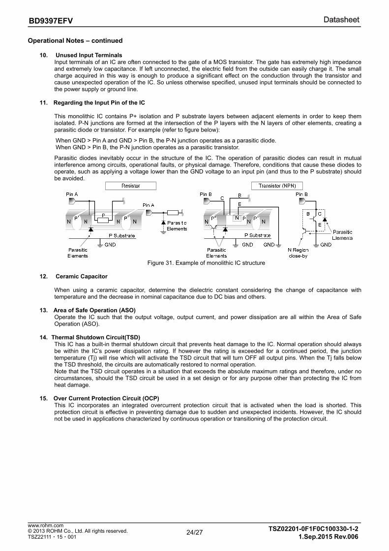
This monolithic IC contains P+ isolation and P substrate layers between adjacent elements in order to keep them isolated. P-N junctions are formed at the intersection of the P layers with the N layers of other elements, creating a parasitic diode or transistor. For example (refer to figure below):
When GND > Pin A and GND > Pin B, the P-N junction operates as a parasitic diode. When GND > Pin B, the P-N junction operates as a parasitic transistor.
Parasitic diodes inevitably occur in the structure of the IC. The operation of parasitic diodes can result in mutual interference among circuits, operational faults, or physical damage. Therefore, conditions that cause these diodes to operate, such as applying a voltage lower than the GND voltage to an input pin (and thus to the P substrate) should be avoided.
Figure 31. Example of monolithic IC structure
12. Ceramic Capacitor When using a ceramic capacitor, determine the dielectric constant considering the change of capacitance with temperature and the decrease in nominal capacitance due to DC bias and others.
13. Area of Safe Operation (ASO)
Operate the IC such that the output voltage, output current, and power dissipation are all within the Area of Safe Operation (ASO).
14. Thermal Shutdown Circuit(TSD)
This IC has a built-in thermal shutdown circuit that prevents heat damage to the IC. Normal operation should always be within the IC’s power dissipation rating. If however the rating is exceeded for a continued period, the junction temperature (Tj) will rise which will activate the TSD circuit that will turn OFF all output pins. When the Tj falls below the TSD threshold, the circuits are automatically restored to normal operation. Note that the TSD circuit operates in a situation that exceeds the absolute maximum ratings and therefore, under no circumstances, should the TSD circuit be used in a set design or for any purpose other than protecting the IC from heat damage.
15. Over Current Protection Circuit (OCP)
This IC incorporates an integrated overcurrent protection circuit that is activated when the load is shorted. This protection circuit is effective in preventing damage due to sudden and unexpected incidents. However, the IC should not be used in applications characterized by continuous operation or transitioning of the protection circuit.

DatasheetDatasheet
25/27 TSZ02201-0F1F0C100330-1-2© 2013 ROHM Co., Ltd. All rights reserved.
1.Sep.2015 Rev.006
www.rohm.com
TSZ22111・15・001
BD9397EFV
Ordering Information
B D 9 3 9 7 E F V - E2
Part Number Package EFV:HTSSOP-B
Packaging and forming specification E2: Embossed tape and reel
Marking Diagram
HTSSOP-B40 (TOP VIEW)
BD9397EFV
Part Number Marking
LOT Number
1PIN MARK

DatasheetDatasheet
26/27 TSZ02201-0F1F0C100330-1-2© 2013 ROHM Co., Ltd. All rights reserved.
1.Sep.2015 Rev.006
www.rohm.com
TSZ22111・15・001
BD9397EFV
Physical Dimension, Tape and Reel Information
Package Name HTSSOP-B40
∗ Order quantity needs to be multiple of the minimum quantity.
<Tape and Reel information>
Embossed carrier tape (with dry pack)Tape
Quantity
Direction of feed
The direction is the 1pin of product is at the upper left when you hold reel on the left hand and you pull out the tape on the right hand
2000pcs
E2
( )
Direction of feed
Reel1pin

DatasheetDatasheet
27/27 TSZ02201-0F1F0C100330-1-2© 2013 ROHM Co., Ltd. All rights reserved.
1.Sep.2015 Rev.006
www.rohm.com
TSZ22111・15・001
BD9397EFV
Revision History
Date Revision Changes
9.Jan.2014 001 Draft Version
10.Mar.2014 002 p.5 1.3 Pin Descriptions No.11-16 LED1-LED6 rating -0.3 to 60 [V] → -0.3 to 50 [V]
26.May.2014 003
p.3 Short circuit protection voltage add condition(FAILMODE=3V) p.13 UVLO detection condition UVLO<2.4V→2.3V p.14 UVLO detection condition UVLO<2.4V→2.3V SCP detection condition OVP<0.2V→0.79V
release condition OVP>0.2V→0.79V
22.Dec.2014 004 p.2 Pin Configuration 37pin LPS→LSP
2.Jul.2015 005 p.14 3.3.2 List of the protection function modify table’s contents
1.Sep.2015 006 p.13,14 The detailed timing condition for protections is added.

DatasheetDatasheet
Notice-PGA-E Rev.001© 2015 ROHM Co., Ltd. All rights reserved.
Notice Precaution on using ROHM Products
1. Our Products are designed and manufactured for application in ordinary electronic equipments (such as AV equipment, OA equipment, telecommunication equipment, home electronic appliances, amusement equipment, etc.). If you intend to use our Products in devices requiring extremely high reliability (such as medical equipment (Note 1), transport equipment, traffic equipment, aircraft/spacecraft, nuclear power controllers, fuel controllers, car equipment including car accessories, safety devices, etc.) and whose malfunction or failure may cause loss of human life, bodily injury or serious damage to property (“Specific Applications”), please consult with the ROHM sales representative in advance. Unless otherwise agreed in writing by ROHM in advance, ROHM shall not be in any way responsible or liable for any damages, expenses or losses incurred by you or third parties arising from the use of any ROHM’s Products for Specific Applications.
(Note1) Medical Equipment Classification of the Specific Applications JAPAN USA EU CHINA
CLASSⅢ CLASSⅢ
CLASSⅡb CLASSⅢ
CLASSⅣ CLASSⅢ
2. ROHM designs and manufactures its Products subject to strict quality control system. However, semiconductor
products can fail or malfunction at a certain rate. Please be sure to implement, at your own responsibilities, adequate safety measures including but not limited to fail-safe design against the physical injury, damage to any property, which a failure or malfunction of our Products may cause. The following are examples of safety measures:
[a] Installation of protection circuits or other protective devices to improve system safety [b] Installation of redundant circuits to reduce the impact of single or multiple circuit failure
3. Our Products are designed and manufactured for use under standard conditions and not under any special or extraordinary environments or conditions, as exemplified below. Accordingly, ROHM shall not be in any way responsible or liable for any damages, expenses or losses arising from the use of any ROHM’s Products under any special or extraordinary environments or conditions. If you intend to use our Products under any special or extraordinary environments or conditions (as exemplified below), your independent verification and confirmation of product performance, reliability, etc, prior to use, must be necessary:
[a] Use of our Products in any types of liquid, including water, oils, chemicals, and organic solvents [b] Use of our Products outdoors or in places where the Products are exposed to direct sunlight or dust [c] Use of our Products in places where the Products are exposed to sea wind or corrosive gases, including Cl2,
H2S, NH3, SO2, and NO2
[d] Use of our Products in places where the Products are exposed to static electricity or electromagnetic waves [e] Use of our Products in proximity to heat-producing components, plastic cords, or other flammable items [f] Sealing or coating our Products with resin or other coating materials [g] Use of our Products without cleaning residue of flux (even if you use no-clean type fluxes, cleaning residue of
flux is recommended); or Washing our Products by using water or water-soluble cleaning agents for cleaning residue after soldering
[h] Use of the Products in places subject to dew condensation
4. The Products are not subject to radiation-proof design. 5. Please verify and confirm characteristics of the final or mounted products in using the Products. 6. In particular, if a transient load (a large amount of load applied in a short period of time, such as pulse. is applied,
confirmation of performance characteristics after on-board mounting is strongly recommended. Avoid applying power exceeding normal rated power; exceeding the power rating under steady-state loading condition may negatively affect product performance and reliability.
7. De-rate Power Dissipation (Pd) depending on Ambient temperature (Ta). When used in sealed area, confirm the actual
ambient temperature. 8. Confirm that operation temperature is within the specified range described in the product specification. 9. ROHM shall not be in any way responsible or liable for failure induced under deviant condition from what is defined in
this document.
Precaution for Mounting / Circuit board design 1. When a highly active halogenous (chlorine, bromine, etc.) flux is used, the residue of flux may negatively affect product
performance and reliability.
2. In principle, the reflow soldering method must be used on a surface-mount products, the flow soldering method must be used on a through hole mount products. If the flow soldering method is preferred on a surface-mount products, please consult with the ROHM representative in advance.
For details, please refer to ROHM Mounting specification

DatasheetDatasheet
Notice-PGA-E Rev.001© 2015 ROHM Co., Ltd. All rights reserved.
Precautions Regarding Application Examples and External Circuits 1. If change is made to the constant of an external circuit, please allow a sufficient margin considering variations of the
characteristics of the Products and external components, including transient characteristics, as well as static characteristics.
2. You agree that application notes, reference designs, and associated data and information contained in this documentare presented only as guidance for Products use. Therefore, in case you use such information, you are solelyresponsible for it and you must exercise your own independent verification and judgment in the use of such informationcontained in this document. ROHM shall not be in any way responsible or liable for any damages, expenses or lossesincurred by you or third parties arising from the use of such information.
Precaution for Electrostatic This Product is electrostatic sensitive product, which may be damaged due to electrostatic discharge. Please take proper caution in your manufacturing process and storage so that voltage exceeding the Products maximum rating will not be applied to Products. Please take special care under dry condition (e.g. Grounding of human body / equipment / solder iron, isolation from charged objects, setting of Ionizer, friction prevention and temperature / humidity control).
Precaution for Storage / Transportation 1. Product performance and soldered connections may deteriorate if the Products are stored in the places where:
[a] the Products are exposed to sea winds or corrosive gases, including Cl2, H2S, NH3, SO2, and NO2 [b] the temperature or humidity exceeds those recommended by ROHM [c] the Products are exposed to direct sunshine or condensation [d] the Products are exposed to high Electrostatic
2. Even under ROHM recommended storage condition, solderability of products out of recommended storage time periodmay be degraded. It is strongly recommended to confirm solderability before using Products of which storage time isexceeding the recommended storage time period.
3. Store / transport cartons in the correct direction, which is indicated on a carton with a symbol. Otherwise bent leadsmay occur due to excessive stress applied when dropping of a carton.
4. Use Products within the specified time after opening a humidity barrier bag. Baking is required before using Products ofwhich storage time is exceeding the recommended storage time period.
Precaution for Product Label QR code printed on ROHM Products label is for ROHM’s internal use only.
Precaution for Disposition When disposing Products please dispose them properly using an authorized industry waste company.
Precaution for Foreign Exchange and Foreign Trade act Since concerned goods might be fallen under listed items of export control prescribed by Foreign exchange and Foreign trade act, please consult with ROHM in case of export.
Precaution Regarding Intellectual Property Rights 1. All information and data including but not limited to application example contained in this document is for reference
only. ROHM does not warrant that foregoing information or data will not infringe any intellectual property rights or any other rights of any third party regarding such information or data.
2. ROHM shall not have any obligations where the claims, actions or demands arising from the combination of theProducts with other articles such as components, circuits, systems or external equipment (including software).
3. No license, expressly or implied, is granted hereby under any intellectual property rights or other rights of ROHM or anythird parties with respect to the Products or the information contained in this document. Provided, however, that ROHMwill not assert its intellectual property rights or other rights against you or your customers to the extent necessary tomanufacture or sell products containing the Products, subject to the terms and conditions herein.
Other Precaution 1. This document may not be reprinted or reproduced, in whole or in part, without prior written consent of ROHM.
2. The Products may not be disassembled, converted, modified, reproduced or otherwise changed without prior writtenconsent of ROHM.
3. In no event shall you use in any way whatsoever the Products and the related technical information contained in theProducts or this document for any military purposes, including but not limited to, the development of mass-destructionweapons.
4. The proper names of companies or products described in this document are trademarks or registered trademarks ofROHM, its affiliated companies or third parties.

DatasheetDatasheet
Notice – WE Rev.001© 2015 ROHM Co., Ltd. All rights reserved.
General Precaution 1. Before you use our Pro ducts, you are requested to care fully read this document and fully understand its contents.
ROHM shall n ot be in an y way responsible or liabl e for fa ilure, malfunction or acci dent arising from the use of a ny ROHM’s Products against warning, caution or note contained in this document.
2. All information contained in this docume nt is current as of the issuing date and subj ect to change without any prior
notice. Before purchasing or using ROHM’s Products, please confirm the la test information with a ROHM sale s representative.
3. The information contained in this doc ument is provi ded on an “as is” basis and ROHM does not warrant that all
information contained in this document is accurate an d/or error-free. ROHM shall not be in an y way responsible or liable for any damages, expenses or losses incurred by you or third parties resulting from inaccuracy or errors of or concerning such information.


![VA2037-LED VA2037m-LED VA2037a-LED LCD Z … · VA2037-LED VA2037m-LED VA2037a-LED LCD Z gªz ] lz e²k¯l jNUºf" Model No. VS15032](https://static.fdocuments.in/doc/165x107/5ba2c11809d3f2d14d8c9a57/va2037-led-va2037m-led-va2037a-led-lcd-z-va2037-led-va2037m-led-va2037a-led.jpg)
