LED Driver with I2C Compatible and 3-wire Serial Interface for...
33
Datasheet ○Product structure:Silicon monolithic integrated circuit ○This product is not designed protection against radioactive rays 1/30 © 2014 ROHM Co., Ltd. All rights reserved. www.rohm.com TSZ22111・14・001 TSZ02201-0G3G0CZ00250-1-2 14.Mar.2016 Rev.003 LED Driver with I 2 C Compatible and 3-wire Serial Interface for 8×16 LEDs in Dot Matrix BU16501KS2 General Description BU16501KS2 is “Matrix LED Driver” that is the most suitable for Home Appliance. It can control 8x16 (128 dot) LED Matrix by internal 8-channel PMOS SWs and 16-channel LED drivers. It can control the brightness in each dot by the setting of the internal register. It supports SPI and I 2 C interface. Features LED Matrix driver (8x16) It has 8-channel PMOS SWs and 16-channel current drivers with 1/8 TDM timing driven sequentially. Put ON/OFF (for every dot) The current drivers can drive from 0 to 20.00mA current with “16” steps(for every dot) The current drivers can drive maximum 42.5mA/Line (ISET=47kΩ) 64 steps of the luminance control by PWM (common setting for all dots) Interface SPI and I 2 C BUS FS mode (max 400 kHz) Compability. For I 2 C mode, I 2 C Device address is selectable (74h or 75h). Thermal Shutdown Pin Configuration(s) Key Specifications Operating power supply voltage range: 2.7V to 5.5V Oscillator frequency: 1.2MHz (Typ.) Operating temperature range: -40℃ to +85℃ Package(s) W(Typ) x D(Typ) x H(Max) SQFP-T52M 12.00mm x 12.00mm x 1.60mm SQFP-T52 12.00mm x 12.00mm x 1.50mm Applications Mobile phone, portable device, home electrical appliance, and general consumer equipment. Device provided with LED display application. LED display. Amusement, Traffic Signboards, hobby, etc. GND4 TEST1 N.C. LED16 LED15 LED14 LEDGND2 LED13 LED12 LED11 LED10 VBAT1 GND5 14 26 CLKIO SYNC VBAT2 VBAT3 IFMODE GND2 RESETB VIO SCL GND3 CE SDA TESTO SW1 SW2 SW3 VINSW SW4 SW5 SW6 SW7 N.C. SW8 ISET LED9 LED8 LED7 LED6 LED5 LEDGND3 N.C. LED4 LED3 LED2 LED1 N.C. 1 13 40 52 LEDGND1 VINSW GND1 27 39
Transcript of LED Driver with I2C Compatible and 3-wire Serial Interface for...

Datasheet
Product structure:Silicon monolithic integrated circuit This product is not designed protection against radioactive rays
1/30 © 2014 ROHM Co., Ltd. All rights reserved. www.rohm.com
TSZ22111・14・001
TSZ02201-0G3G0CZ00250-1-214.Mar.2016 Rev.003
LED Driver with I2C Compatible and 3-wire Serial Interface for 8×16 LEDs in Dot Matrix BU16501KS2
General Description BU16501KS2 is “Matrix LED Driver” that is the most suitable for Home Appliance. It can control 8x16 (128 dot) LED Matrix by internal 8-channel PMOS SWs and 16-channel LED drivers. It can control the brightness in each dot by the setting of the internal register. It supports SPI and I2C interface.
Features
LED Matrix driver (8x16) It has 8-channel PMOS SWs and
16-channel current drivers with 1/8 TDM timing driven sequentially.
Put ON/OFF (for every dot) The current drivers can drive from 0
to 20.00mA current with “16” steps(for every dot)
The current drivers can drive maximum 42.5mA/Line (ISET=47kΩ)
64 steps of the luminance control by PWM (common setting for all dots)
Interface SPI and I2C BUS FS mode (max 400
kHz) Compability. For I2C mode, I2C Device address is
selectable (74h or 75h). Thermal Shutdown
Pin Configuration(s)
Key Specifications Operating power supply voltage range: 2.7V to 5.5V Oscillator frequency: 1.2MHz (Typ.) Operating temperature range: -40 to +85
Package(s) W(Typ) x D(Typ) x H(Max)
SQFP-T52M 12.00mm x 12.00mm x 1.60mm SQFP-T52 12.00mm x 12.00mm x 1.50mm
Applications
Mobile phone, portable device, home electrical appliance, and general consumer equipment. Device provided with LED display application. LED display. Amusement, Traffic Signboards, hobby, etc.
GN
D4
TE
ST
1
N.C
.
LE
D1
6
LE
D1
5
LE
D1
4
LE
DG
ND
2
LE
D1
3
LE
D1
2
LE
D1
1
LE
D1
0
VB
AT
1
GN
D5
14
26CLKIO
SYNC
VBAT2
VBAT3
IFMODE
GND2
RESETB
VIO
SCL
GND3
CE
SDA
TESTO
SW
1
SW
2
SW
3
VIN
SW
SW
4
SW
5
SW
6
SW
7
N.C
.
SW
8
ISET
LED9
LED8
LED7
LED6
LED5
LEDGND3
N.C.
LED4
LED3
LED2
LED1
N.C.
1 13
40
52
LE
DG
ND
1
VIN
SW
GN
D1
2739
2/30
DatasheetDatasheetBU16501KS2
© 2014 ROHM Co., Ltd. All rights reserved. www.rohm.com
TSZ22111・15・001
TSZ02201-0G3G0CZ00250-1-214.Mar.2016 Rev.003
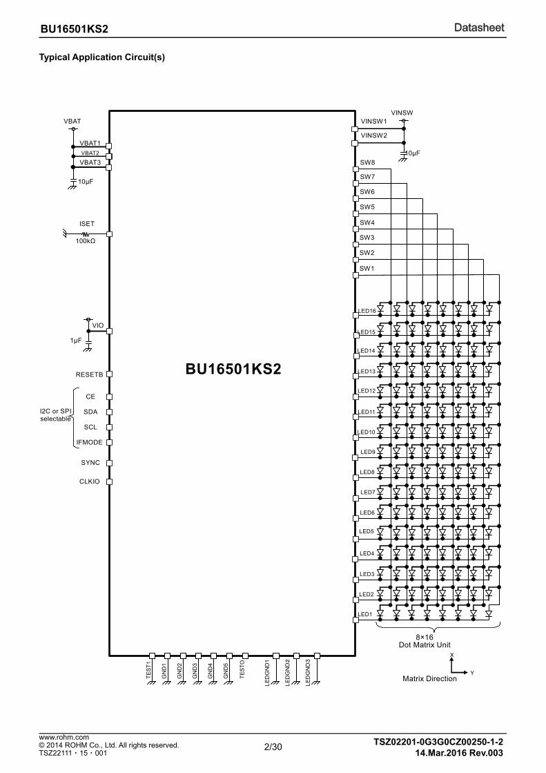
Typical Application Circuit(s)
ISET
LED1
LED2
LED3
LED4
LED5
LED6
LED8
LED9
LED10
LED11
LED13
LED12
LED7
LED14
LED15
LED16
SW1
SW2
SW3
SW4
SW5
SW6
SW7
10μF
8×16 Dot Matrix Unit
100kΩ
TE
ST
1
RESETB
CE
SDA
SCL
IFMODE
SYNC
CLKIO
I2C or SPI selectable
VIO
1µF
GN
D1
GN
D2
GN
D3
GN
D4
TE
ST
O
LE
DG
ND
1
LE
DG
ND
2
VINSW
VBAT2
10µF
VBAT VINSW1
VBAT1
Matrix DirectionY
X
VINSW2
SW8
LE
DG
ND
3
VBAT3
GN
D5
BU16501KS2
3/30
DatasheetDatasheetBU16501KS2
© 2014 ROHM Co., Ltd. All rights reserved. www.rohm.com
TSZ22111・15・001
TSZ02201-0G3G0CZ00250-1-214.Mar.2016 Rev.003
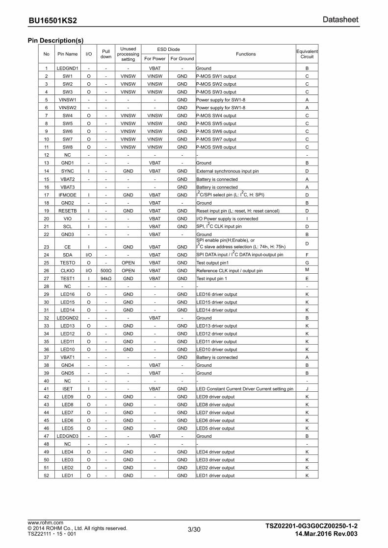
Pin Description(s)
No Pin Name I/O Pull
down
Unused processing
setting
ESD Diode Functions
Equivalent Circuit For Power For Ground
1 LEDGND1 - - - VBAT - Ground B
2 SW1 O - VINSW VINSW GND P-MOS SW1 output C
3 SW2 O - VINSW VINSW GND P-MOS SW2 output C
4 SW3 O - VINSW VINSW GND P-MOS SW3 output C
5 VINSW1 - - - - GND Power supply for SW1-8 A
6 VINSW2 - - - - GND Power supply for SW1-8 A
7 SW4 O - VINSW VINSW GND P-MOS SW4 output C
8 SW5 O - VINSW VINSW GND P-MOS SW5 output C
9 SW6 O - VINSW VINSW GND P-MOS SW6 output C
10 SW7 O - VINSW VINSW GND P-MOS SW7 output C
11 SW8 O - VINSW VINSW GND P-MOS SW8 output C
12 NC - - - - - - -
13 GND1 - - - VBAT - Ground B
14 SYNC I - GND VBAT GND External synchronous input pin D
15 VBAT2 - - - - GND Battery is connected A
16 VBAT3 - - - GND Battery is connected A
17 IFMODE I - GND VBAT GND I2C/SPI select pin (L: I
2C, H: SPI) D
18 GND2 - - - VBAT - Ground B
19 RESETB I - GND VBAT GND Reset input pin (L: reset, H: reset cancel) D
20 VIO - - - VBAT GND I/O Power supply is connected I
21 SCL I - - VBAT GND SPI, I2C CLK input pin D
22 GND3 - - - VBAT - Ground B
23 CE I - GND VBAT GND
SPI enable pin(H;Enable), or
I2C slave address selection (L: 74h, H: 75h)
D
24 SDA I/O - - VBAT GND SPI DATA input / I2C DATA input-output pin F
25 TESTO O - OPEN VBAT GND Test output pin1 G
26 CLKIO I/O 500Ω OPEN VBAT GND Reference CLK input / output pin M
27 TEST1 I 94kΩ GND VBAT GND Test input pin 1 E
28 NC - - - - - - -
29 LED16 O - GND - GND LED16 driver output K
30 LED15 O - GND - GND LED15 driver output K
31 LED14 O - GND - GND LED14 driver output K
32 LEDGND2 - - - VBAT - Ground B
33 LED13 O - GND - GND LED13 driver output K
34 LED12 O - GND - GND LED12 driver output K
35 LED11 O - GND - GND LED11 driver output K
36 LED10 O - GND - GND LED10 driver output K
37 VBAT1 - - - - GND Battery is connected A
38 GND4 - - - VBAT - Ground B
39 GND5 - - - VBAT - Ground B
40 NC - - - - - - -
41 ISET I - - VBAT GND LED Constant Current Driver Current setting pin J
42 LED9 O - GND - GND LED9 driver output K
43 LED8 O - GND - GND LED8 driver output K
44 LED7 O - GND - GND LED7 driver output K
45 LED6 O - GND - GND LED6 driver output K
46 LED5 O - GND - GND LED5 driver output K
47 LEDGND3 - - - VBAT - Ground B
48 NC - - - - - - -
49 LED4 O - GND - GND LED4 driver output K
50 LED3 O - GND - GND LED3 driver output K
51 LED2 O - GND - GND LED2 driver output K
52 LED1 O - GND - GND LED1 driver output K

4/30
DatasheetDatasheetBU16501KS2
© 2014 ROHM Co., Ltd. All rights reserved. www.rohm.com
TSZ22111・15・001
TSZ02201-0G3G0CZ00250-1-214.Mar.2016 Rev.003
Pin ESD Type
VBATB VIO VBAT D
VBAT J
VINSWC VINSW
VIO VBAT E VIOVBAT F VBAT H
K
A
VBAT I VIO VBAT M VIO
VBATG VIO
Figure 1. Pin ESD Type

5/30
DatasheetDatasheetBU16501KS2
© 2014 ROHM Co., Ltd. All rights reserved. www.rohm.com
TSZ22111・15・001
TSZ02201-0G3G0CZ00250-1-214.Mar.2016 Rev.003
Absolute Maximum Ratings (Ta=25) Parameter Symbol Limits Unit
Terminal voltage VMAX -0.3 to +7 V
Power Dissipation (note1) Pd 1.30 W
Operating Temperature Range Topr -40 to +85
Storage Temperature Range Tstg -55 to +125 (Note1) Power dissipation deleting is 13mW/°C, when it’s used in over 25°C (ROHM’s standard one layer board has been mounted.) The power dissipation of the IC has to be less than the one of the package. Caution: Operating the IC over the absolute maximum ratings may damage the IC. The damage can either be a short circuit between pins or an open circuit between pins and the internal circuitry. Therefore, it is important to consider circuit protection measures, such as adding a fuse, in case the IC is operated over the absolute maximum ratings.
Recommended Operating Ratings (Ta=-40 to 85)
Parameter Symbol Limits Unit
VBAT input voltage VBAT 2.7 to 5.5 V
VINSW input voltage VINSW 2.7 to 5.5 V
VIO pin voltage VIO 1.65 to 5.5 V
Electrical Characteristics
(Unless otherwise specified, Ta=25, VBAT=5.0V, VINSW=5.0V, VIO=5.0V)
Parameter Symbol Limit
Unit Condition Min Typ Max
[ Circuit Current ]
VBAT Circuit current 1 IBAT1 - 0 3.0 μA RESETB=0V, VIO=0V
VBAT Circuit current 2 IBAT2 - 0.7 5.0 μA RESETB=0V, VIO=5.0V
VBAT Circuit current 3 IBAT3 - 2.1 3.5 mA When LED1-16 are active with 10.67mA settings.
[ UVLO ]
UVLO Threshold VUVLO - 2.1 2.5 V VBAT falling
UVLO Hysteresis VHYUVLO 50 - - mV
[ LED Driver ] (LED1-16)
Maximum output current ILEDMax1 - 20.00 - mA LED1-16 ,ISET=100kΩ
ILEDMax2 - 42.50 - mA LED1-16 ,ISET=47kΩ
Output current ILED -7.0 - +7.0 % I=10.67mA setting, VLED=1V
ISET=100kΩ
LED current Matching ILEDMT - - 5 % ILEDMT= (ILEDMax-ILEDMin)/(ILEDMax+ILEDMin) I=10.67mA setting, VLED=1V, ISET=100kΩ
Driver pin voltage range VLED1 0.2 - VBAT
- 1.4 V LED1-16 ,ISET=100kΩ
LED OFF Leak current ILKLED - - 1.0 μA
[ PMOS switch ]
Leak current at OFF ILEAKP - - 1.0 μA
Resistor at ON RonP - 1.0 - Ω Isw=160mA, VINSW=5.0V
[ OSC ]
OSC frequency fosc 0.96 1.2 1.44 MHz
[ CE, SYNC, IFMODE ]
L level input voltage VIL1 -0.3 - 0.25 x
VIO V
H level input voltage VIH1 0.75 x
VIO -
VIO
+0.3 V
input current Iin1 - 0 1 μA Input voltage = from (0.1 x VIO) to (0.9 x VIO)

6/30
DatasheetDatasheetBU16501KS2
© 2014 ROHM Co., Ltd. All rights reserved. www.rohm.com
TSZ22111・15・001
TSZ02201-0G3G0CZ00250-1-214.Mar.2016 Rev.003
Electrical Characteristics - continued
Parameter Symbol Limit
Unit Condition Min Typ Max
[ SDA, SCL ]
L level input voltage VIL2 -0.3 - 0.25×VIO V
H level input voltage VIH2 0.75×VIO - VIO+0.3 V
Input hysteresis Vhys 0.05×VIO - - V
L level output voltage (for SDA pin)
VOL2 - - 0.3 V IOL=3mA
Input current Iin2 -3 - 3 μAInput voltage = from (0.1 x VIO) to (0.9 x VIO)
[ RESETB ]
L level input voltage VIL3 -0.3 - 0.25×VIO V
H level input voltage VIH3 0.75×VIO - VIO+0.3 V
Input current Iin3 - 0 1 μAInput voltage = from (0.1 x VIO) to (0.9 x VIO)
【CLKIO(output)】
L level output voltage VOL1 - - 0.4 V IOL=2mA
H level output voltage VOH1 VIO-0.4 - - V IOH=-2mA
【CLKIO(input)】
L level input voltage VIL4 -0.3 - 0.25×VIO V
H level input voltage VIH4 0.75×VIO - VIO+0.3 V
Input current Iin4 - 10 20 μA Input voltage =5.0V
(Unless otherwise specified, Ta=25°C, VBAT=5.0V, VINSW=5.0V, VIO=5.0V)
Parameter Symbol Limit
Unit Condition Min Typ Max
SCL cycle time tscyc 76 - - ns
H period of SCL cycle Twhc 35 - - ns
L period of SCL cycle Twlc 35 - - ns
SDA setup time Tss 38 - - ns
SDA hold time Tsh 38 - - ns
Write interval
Tcsw
38 - - ns
Write interval (after RAM accsess)
2.1 - - μs (Note 1)
ECLK x 2 - - s (Note 2)
CE setup time Tcss 55 - - ns
CE hold time Tcgh 48 - - ns (Note 1) When it used internal clock. (Note 2) When it used external clock. (ECLK means the cycle of external clock)
(Unless otherwise specified, Ta=25 oC, VBAT=5.0V, VINSW=5.0V, VIO=5.0V)
Parameter SymbolStandard-mode Fast-mode
Unit Min Typ Max Min Typ Max
【I2C BUS format】 SCL clock frequency fSCL 0 - 100 0 - 400 kHz
LOW period of the SCL clock tLOW 4.7 - - 1.3 - - μs HIGH period of the SCL clock tHIGH 4.0 - - 0.6 - - μs Hold time (repeated) START condition After this period, the first clock is generated tHD;STA 4.0 - - 0.6 - - μs
Set-up time for a repeated START condition
tSU;STA 4.7 - - 0.6 - - μs
Data hold time tHD;DAT 0 - 3.45 0 - 0.9 μs Data set-up time tSU;DAT 250 - - 100 - - ns Set-up time for STOP condition tSU;STO 4.0 - - 0.6 - - μs Bus free time between a STOP and START condition
tBUF 4.7 - - 1.3 - - μs

7/30
DatasheetDatasheetBU16501KS2
© 2014 ROHM Co., Ltd. All rights reserved. www.rohm.com
TSZ22111・15・001
TSZ02201-0G3G0CZ00250-1-214.Mar.2016 Rev.003
PWM
LED1TDM
TDMLED2
TDMLED3
TDMLED4
TDM
LED5
TDMLED6
TDM
TDMLED8
TDMLED9
TDMLED10
TDMLED11
TDM
TDMLED13
LED12
LED7
TDMLED14
TDMLED15
TDMLED16
SW1 T00
SW2 T01
SW3 T02
T03
T04
T05
T06
SW4
SW5
SW6
SW7
VREF
IREF
Logic TDMISET
Max 42.5mA/ch64 steps DC
TE
ST
1
RESETB
CE
SDA
SCL
IFMODE
SYNC
CLKIO
VIO
I/O SPI / I2C interface
Digital Control
Level
Shift
GN
D1
GN
D2
GN
D3
GN
D4
TE
ST
O
LE
DG
ND
1
LE
DG
ND
2
OSC
VBAT2
VINSW1
VBAT1VINSW2
T07SW8
LE
DG
ND
3
VBAT3
GN
D5
Block Diagram

8/30
DatasheetDatasheetBU16501KS2
© 2014 ROHM Co., Ltd. All rights reserved. www.rohm.com
TSZ22111・15・001
TSZ02201-0G3G0CZ00250-1-214.Mar.2016 Rev.003
Serial Interface 1. SPI format
・ When IFMODE is set to “H”, it can interface with SPI format. ・The serial interface is four terminals (serial clock terminal (SCL), serial data input terminal (SDA), and chip selection
input terminal (CE)).
(1)Write operation ・ Data is taken into an internal shift register with rising edge of SCL. (Max of the frequency is 13MHz.) ・ The receive data becomes enable in the “H" section of CE. (Active “H".) ・ The transmit data is forwarded (with MSB-First) in the order of write command “0”(1bit), the control register address
(7bit) and data (8bit).
Figure 2. Writing format
(2)Timing diagram
Figure 3. Timing diagram (SPI format)
2. I2C BUS format
When IFMODE is set to “L”, it can interface with I2C BUS format.
(1) Slave address CE A7 A6 A5 A4 A3 A2 A1 R/W
L 1 1 1 0 1 0 0 0
H 1 1 1 0 1 0 1
(2) Bit Transfer SCL transfers 1-bit data during H. During H of SCL, SDA cannot be changed at the time of bit transfer. If SDA changes while SCL is H, START conditions or STOP conditions will occur and it will be interpreted as a control signal.
SDA
SCL
SDA a state of stability:Data are effective
SDA It can change
Figure 4. Bit transfer (I2C format)
CE
SCL
SDA W A6 A5 A4 A3 A2 A1 A0 D4 D3 D2 D1 D0 D7 D6 D5
twlc
CE
SCL
SDA
tcsw
twhc
tcss tscyc
tss tsh
tcgh
9/30
DatasheetDatasheetBU16501KS2
© 2014 ROHM Co., Ltd. All rights reserved. www.rohm.com
TSZ22111・15・001
TSZ02201-0G3G0CZ00250-1-214.Mar.2016 Rev.003
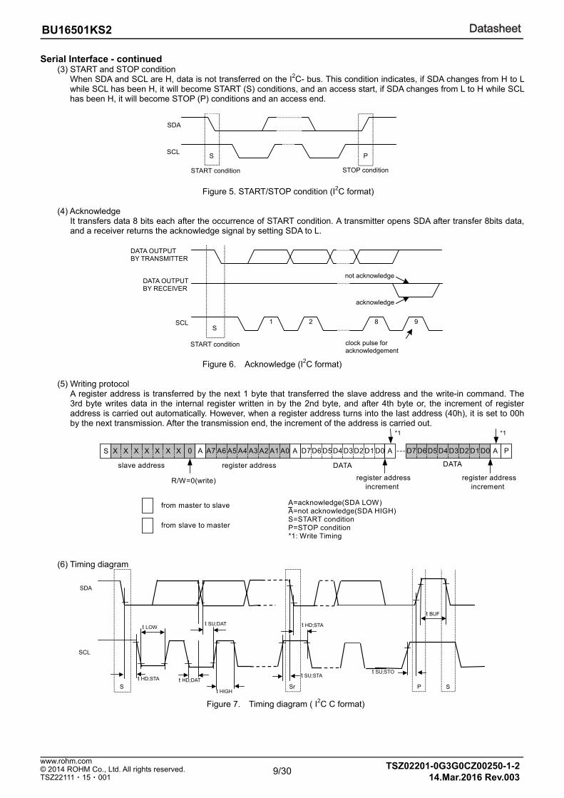
Serial Interface - continued (3) START and STOP condition
When SDA and SCL are H, data is not transferred on the I2C- bus. This condition indicates, if SDA changes from H to L while SCL has been H, it will become START (S) conditions, and an access start, if SDA changes from L to H while SCL has been H, it will become STOP (P) conditions and an access end.
SDA
SCL S P
START condition STOP condition Figure 5. START/STOP condition (I2C format)
(4) Acknowledge
It transfers data 8 bits each after the occurrence of START condition. A transmitter opens SDA after transfer 8bits data, and a receiver returns the acknowledge signal by setting SDA to L.
1 2 8 9
DATA OUTPUT BY TRANSMITTER
DATA OUTPUT BY RECEIVER
acknowledge
not acknowledge
S
START condition clock pulse for acknowledgement
SCL
Figure 6. Acknowledge (I2C format)
(5) Writing protocol
A register address is transferred by the next 1 byte that transferred the slave address and the write-in command. The 3rd byte writes data in the internal register written in by the 2nd byte, and after 4th byte or, the increment of register address is carried out automatically. However, when a register address turns into the last address (40h), it is set to 00h by the next transmission. After the transmission end, the increment of the address is carried out.
S A A A P
register addressslave address
from master to slave
from slave to master
R/W=0(write)
DATA
AD7 D6 D5 D4 D3 D2 D1 D0 D7 D6 D5 D4 D3 D2 D1 D0A7 A6 A5 A4 A3 A2 A1 A00 X X X X X X X
*1 *1
DATA
A=acknowledge(SDA LOW)A=not acknowledge(SDA HIGH)S=START conditionP=STOP condition*1: Write Timing
register address increment
register addressincrement
(6) Timing diagram
SDA
SCL
t SU;DAT t LOW
S Sr P S
t BUF
t HD;STA
t SU;STA
t HIGH
t HD;STA t HD;DAT
t SU;STO
Figure 7. Timing diagram ( I2C C format)
10/30
DatasheetDatasheetBU16501KS2
© 2014 ROHM Co., Ltd. All rights reserved. www.rohm.com
TSZ22111・15・001
TSZ02201-0G3G0CZ00250-1-214.Mar.2016 Rev.003
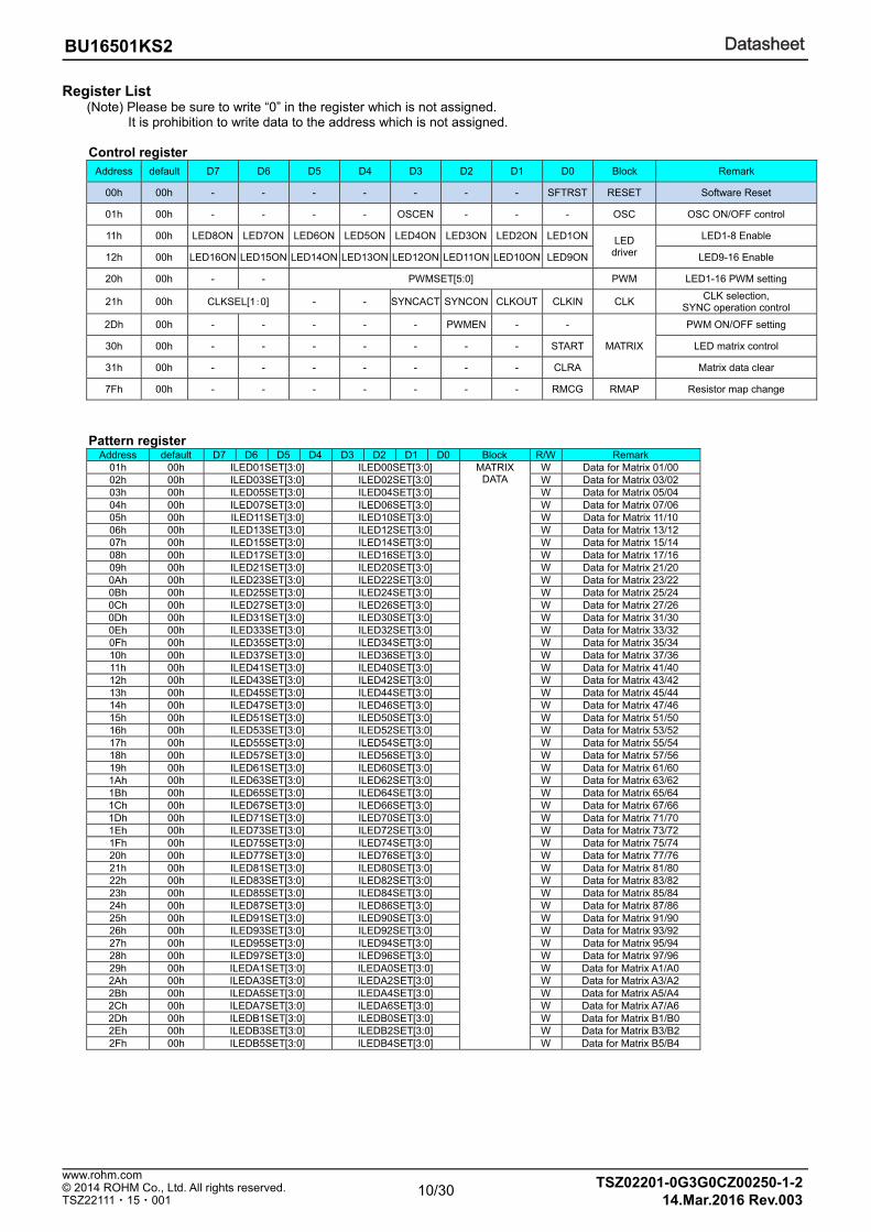
Register List (Note) Please be sure to write “0” in the register which is not assigned.
It is prohibition to write data to the address which is not assigned. Control register
Address default D7 D6 D5 D4 D3 D2 D1 D0 Block Remark
00h 00h - - - - - - - SFTRST RESET Software Reset
01h 00h - - - - OSCEN - - - OSC OSC ON/OFF control
11h 00h LED8ON LED7ON LED6ON LED5ON LED4ON LED3ON LED2ON LED1ON LED driver
LED1-8 Enable
12h 00h LED16ON LED15ON LED14ON LED13ON LED12ON LED11ON LED10ON LED9ON LED9-16 Enable
20h 00h - - PWMSET[5:0] PWM LED1-16 PWM setting
21h 00h CLKSEL[1:0] - - SYNCACT SYNCON CLKOUT CLKIN CLK CLK selection,
SYNC operation control
2Dh 00h - - - - - PWMEN - -
MATRIX
PWM ON/OFF setting
30h 00h - - - - - - - START LED matrix control
31h 00h - - - - - - - CLRA Matrix data clear
7Fh 00h - - - - - - - RMCG RMAP Resistor map change
Pattern register Address default D7 D6 D5 D4 D3 D2 D1 D0 Block R/W Remark
01h 00h ILED01SET[3:0] ILED00SET[3:0] MATRIX DATA
W Data for Matrix 01/00 02h 00h ILED03SET[3:0] ILED02SET[3:0] W Data for Matrix 03/02 03h 00h ILED05SET[3:0] ILED04SET[3:0] W Data for Matrix 05/04 04h 00h ILED07SET[3:0] ILED06SET[3:0] W Data for Matrix 07/06 05h 00h ILED11SET[3:0] ILED10SET[3:0] W Data for Matrix 11/10 06h 00h ILED13SET[3:0] ILED12SET[3:0] W Data for Matrix 13/12 07h 00h ILED15SET[3:0] ILED14SET[3:0] W Data for Matrix 15/14 08h 00h ILED17SET[3:0] ILED16SET[3:0] W Data for Matrix 17/16 09h 00h ILED21SET[3:0] ILED20SET[3:0] W Data for Matrix 21/20 0Ah 00h ILED23SET[3:0] ILED22SET[3:0] W Data for Matrix 23/22 0Bh 00h ILED25SET[3:0] ILED24SET[3:0] W Data for Matrix 25/24 0Ch 00h ILED27SET[3:0] ILED26SET[3:0] W Data for Matrix 27/26 0Dh 00h ILED31SET[3:0] ILED30SET[3:0] W Data for Matrix 31/30 0Eh 00h ILED33SET[3:0] ILED32SET[3:0] W Data for Matrix 33/32 0Fh 00h ILED35SET[3:0] ILED34SET[3:0] W Data for Matrix 35/34 10h 00h ILED37SET[3:0] ILED36SET[3:0] W Data for Matrix 37/36 11h 00h ILED41SET[3:0] ILED40SET[3:0] W Data for Matrix 41/40 12h 00h ILED43SET[3:0] ILED42SET[3:0] W Data for Matrix 43/42 13h 00h ILED45SET[3:0] ILED44SET[3:0] W Data for Matrix 45/44 14h 00h ILED47SET[3:0] ILED46SET[3:0] W Data for Matrix 47/46 15h 00h ILED51SET[3:0] ILED50SET[3:0] W Data for Matrix 51/50 16h 00h ILED53SET[3:0] ILED52SET[3:0] W Data for Matrix 53/52 17h 00h ILED55SET[3:0] ILED54SET[3:0] W Data for Matrix 55/54 18h 00h ILED57SET[3:0] ILED56SET[3:0] W Data for Matrix 57/56 19h 00h ILED61SET[3:0] ILED60SET[3:0] W Data for Matrix 61/60 1Ah 00h ILED63SET[3:0] ILED62SET[3:0] W Data for Matrix 63/62 1Bh 00h ILED65SET[3:0] ILED64SET[3:0] W Data for Matrix 65/64 1Ch 00h ILED67SET[3:0] ILED66SET[3:0] W Data for Matrix 67/66 1Dh 00h ILED71SET[3:0] ILED70SET[3:0] W Data for Matrix 71/70 1Eh 00h ILED73SET[3:0] ILED72SET[3:0] W Data for Matrix 73/72 1Fh 00h ILED75SET[3:0] ILED74SET[3:0] W Data for Matrix 75/74 20h 00h ILED77SET[3:0] ILED76SET[3:0] W Data for Matrix 77/76 21h 00h ILED81SET[3:0] ILED80SET[3:0] W Data for Matrix 81/80 22h 00h ILED83SET[3:0] ILED82SET[3:0] W Data for Matrix 83/82 23h 00h ILED85SET[3:0] ILED84SET[3:0] W Data for Matrix 85/84 24h 00h ILED87SET[3:0] ILED86SET[3:0] W Data for Matrix 87/86 25h 00h ILED91SET[3:0] ILED90SET[3:0] W Data for Matrix 91/90 26h 00h ILED93SET[3:0] ILED92SET[3:0] W Data for Matrix 93/92 27h 00h ILED95SET[3:0] ILED94SET[3:0] W Data for Matrix 95/94 28h 00h ILED97SET[3:0] ILED96SET[3:0] W Data for Matrix 97/96 29h 00h ILEDA1SET[3:0] ILEDA0SET[3:0] W Data for Matrix A1/A0 2Ah 00h ILEDA3SET[3:0] ILEDA2SET[3:0] W Data for Matrix A3/A2 2Bh 00h ILEDA5SET[3:0] ILEDA4SET[3:0] W Data for Matrix A5/A4 2Ch 00h ILEDA7SET[3:0] ILEDA6SET[3:0] W Data for Matrix A7/A6 2Dh 00h ILEDB1SET[3:0] ILEDB0SET[3:0] W Data for Matrix B1/B0 2Eh 00h ILEDB3SET[3:0] ILEDB2SET[3:0] W Data for Matrix B3/B2 2Fh 00h ILEDB5SET[3:0] ILEDB4SET[3:0] W Data for Matrix B5/B4
11/30
DatasheetDatasheetBU16501KS2
© 2014 ROHM Co., Ltd. All rights reserved. www.rohm.com
TSZ22111・15・001
TSZ02201-0G3G0CZ00250-1-214.Mar.2016 Rev.003
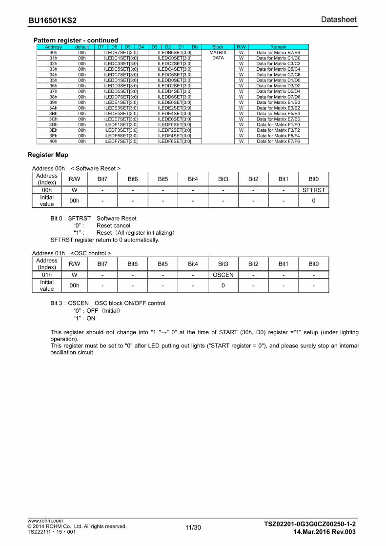
Pattern register - continued Address default D7 D6 D5 D4 D3 D2 D1 D0 Block R/W Remark
30h 00h ILEDB7SET[3:0] ILEDB6SET[3:0] MATRIX DATA
W Data for Matrix B7/B6 31h 00h ILEDC1SET[3:0] ILEDC0SET[3:0] W Data for Matrix C1/C0 32h 00h ILEDC3SET[3:0] ILEDC2SET[3:0] W Data for Matrix C3/C2 33h 00h ILEDC5SET[3:0] ILEDC4SET[3:0] W Data for Matrix C5/C4 34h 00h ILEDC7SET[3:0] ILEDC6SET[3:0] W Data for Matrix C7/C6 35h 00h ILEDD1SET[3:0] ILEDD0SET[3:0] W Data for Matrix D1/D0 36h 00h ILEDD3SET[3:0] ILEDD2SET[3:0] W Data for Matrix D3/D2 37h 00h ILEDD5SET[3:0] ILEDD4SET[3:0] W Data for Matrix D5/D4 38h 00h ILEDD7SET[3:0] ILEDD6SET[3:0] W Data for Matrix D7/D6 39h 00h ILEDE1SET[3:0] ILEDE0SET[3:0] W Data for Matrix E1/E0 3Ah 00h ILEDE3SET[3:0] ILEDE2SET[3:0] W Data for Matrix E3/E2 3Bh 00h ILEDE5SET[3:0] ILEDE4SET[3:0] W Data for Matrix E5/E4 3Ch 00h ILEDE7SET[3:0] ILEDE6SET[3:0] W Data for Matrix E7/E6 3Dh 00h ILEDF1SET[3:0] ILEDF0SET[3:0] W Data for Matrix F1/F0 3Eh 00h ILEDF3SET[3:0] ILEDF2SET[3:0] W Data for Matrix F3/F2 3Fh 00h ILEDF5SET[3:0] ILEDF4SET[3:0] W Data for Matrix F5/F4 40h 00h ILEDF7SET[3:0] ILEDF6SET[3:0] W Data for Matrix F7/F6
Register Map
Address 00h < Software Reset > Address (Index)
R/W Bit7 Bit6 Bit5 Bit4 Bit3 Bit2 Bit1 Bit0
00h W - - - - - - - SFTRSTInitial value
00h - - - - - - - 0
Bit 0:SFTRST Software Reset
“0” : Reset cancel “1” : Reset(All register initializing)
SFTRST register return to 0 automatically.
Address 01h <OSC control > Address (Index)
R/W Bit7 Bit6 Bit5 Bit4 Bit3 Bit2 Bit1 Bit0
01h W - - - - OSCEN - - - Initial value
00h - - - - 0 - - -
Bit 3:OSCEN OSC block ON/OFF control
“0”:OFF(Initial) “1”:ON
This register should not change into "1 "→" 0" at the time of START (30h, D0) register ="1" setup (under lighting operation). This register must be set to "0" after LED putting out lights ("START register = 0"), and please surely stop an internal oscillation circuit.

12/30
DatasheetDatasheetBU16501KS2
© 2014 ROHM Co., Ltd. All rights reserved. www.rohm.com
TSZ22111・15・001
TSZ02201-0G3G0CZ00250-1-214.Mar.2016 Rev.003
Register Map - continued Address 11h < LED1-8 Enable >
Address (Index)
R/W Bit7 Bit6 Bit5 Bit4 Bit3 Bit2 Bit1 Bit0
11h W LED8ON LED7ON LED6ON LED5ON LED4ON LED3ON LED2ON LED1ONInitial value
00h 0 0 0 0 0 0 0 0
Bit 0:LED1ON LED1 ON/OFF setting “0”:LED1 OFF(initial) “1”:LED1 ON Bit 1:LED2ON LED2 ON/OFF setting “0”:LED2 OFF(initial) “1”:LED2 ON Bit 2:LED3ON LED3 ON/OFF setting “0”:LED3 OFF(initial) “1”:LED3 ON Bit 3:LED4ON LED4 ON/OFF setting “0”:LED4 OFF(initial) “1”:LED4 ON Bit 4:LED5ON LED5 ON/OFF setting “0”:LED5 OFF(initial) “1”:LED5 ON Bit 5:LED6ON LED6 ON/OFF setting “0”:LED6 OFF(initial) “1”:LED6 ON Bit 6:LED7ON LED7 ON/OFF setting “0”:LED7 OFF(initial) “1”:LED7 ON Bit 7:LED8ON LED8 ON/OFF setting “0”:LED8 OFF(initial) “1”:LED8 ON
(Note) Current setting follows ILEDXXSET[3:0] register.

13/30
DatasheetDatasheetBU16501KS2
© 2014 ROHM Co., Ltd. All rights reserved. www.rohm.com
TSZ22111・15・001
TSZ02201-0G3G0CZ00250-1-214.Mar.2016 Rev.003
Register Map - continued Address 12h < LED9-16 Enable >
Address (Index)
R/W Bit7 Bit6 Bit5 Bit4 Bit3 Bit2 Bit1 Bit0
12h W LED16
ON LED15
ON LED14
ON LED13
ON LED12
ON LED11
ON LED10
ON LED9 ON
Initial value
00h 0 0 0 0 0 0 0 0
Bit 0:LED9ON LED9 ON/OFF setting “0”:LED9 OFF(initial) “1”:LED9 ON Bit 1:LED10ON LED10 ON/OFF setting “0”:LED10 OFF(initial) “1”:LED10 ON Bit 2:LED11ON LED11 ON/OFF setting “0”:LED11 OFF(initial) “1”:LED11 ON Bit 3:LED12ON LED12 ON/OFF setting “0”:LED12 OFF(initial) “1”:LED12 ON Bit 4:LED13ON LED13 ON/OFF setting “0”:LED13 OFF(initial) “1”:LED13 ON Bit 5:LED14ON LED14 ON/OFF setting “0”:LED14 OFF(initial) “1”:LED14 ON Bit 6:LED15ON LED15 ON/OFF setting “0”:LED15 OFF(initial) “1”:LED15 ON Bit 7:LED16ON LED16 ON/OFF setting “0”:LED16 OFF(initial) “1”:LED16 ON
(Note) Current setting follows ILEDXXSET[3:0] register.

14/30
DatasheetDatasheetBU16501KS2
© 2014 ROHM Co., Ltd. All rights reserved. www.rohm.com
TSZ22111・15・001
TSZ02201-0G3G0CZ00250-1-214.Mar.2016 Rev.003
Register Map - continued Address 20h < LED1-16 PWM setting >
Address (Index)
R/W Bit7 Bit6 Bit5 Bit4 Bit3 Bit2 Bit1 Bit0
20h W - - PWMSET [5:0] Initial value
00h - - 0 0 0 0 0 0
Bit 5-0:PWMSET[5:0] LED1-16 PWM DUTY setting “000000”: 0/63=0%(initial) “000001”: 1/63=1.59% : : “100000”:32/63=50.8% : : “111110”:62/63=98.4% “111111”:63/63=100%
(Note)Please refer to Description of operation, chapter 2
Address 21h <Clock control / SYNC operation control>
Address (Index)
R/W Bit7 Bit6 Bit5 Bit4 Bit3 Bit2 Bit1 Bit0
21h W CLKSEL[1:0] - - SYNCACT SYNCON CLKOUT CLKIN Initial value 00h 0 0 - - 0 0 0 0
Bit 0:CLKIN Selection CLK for PWM control “0”:Internal OSC (initial) “1”:External CLK input (to CLKIO pin)
Bit 1:CLKOUT Output CLK enable “0”:CLK is not output (initial) “1”:Output selected CLK from CLKIO pin
As for CLKIN & CLKOUT, setting change is forbidden under OSCEN (01h, D3) register =”1” and also under clock input to CLKIO terminal.
Bit 2:SYNCON SYNC operation enable “0”:Disable SYNC operation (initial) “1”:SYNC pin control LED driver ON/OFF
Bit 3:SYNCACT SYNC operation setting “0”:When SYNC pin is “L”, LED drivers are ON (initial) “1”:When SYNC pin is “H”, LED drivers are ON
Bit 7-6:CLKSEL[1:0] Select Clock Frequency
“00”:1.2MHz (initial) “01”:300kHz “10”:150kHz “11”:37.5kHz
15/30
DatasheetDatasheetBU16501KS2
© 2014 ROHM Co., Ltd. All rights reserved. www.rohm.com
TSZ22111・15・001
TSZ02201-0G3G0CZ00250-1-214.Mar.2016 Rev.003
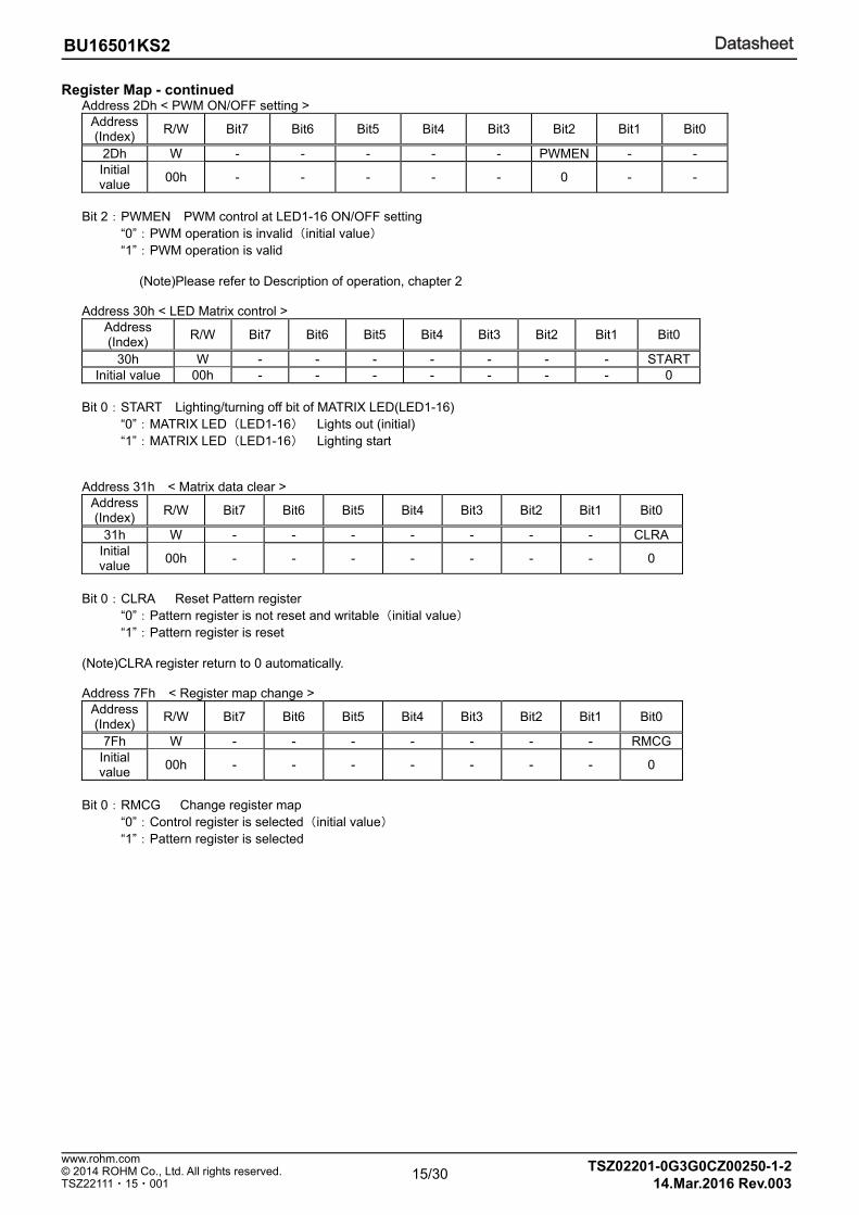
Register Map - continued Address 2Dh < PWM ON/OFF setting >
Address (Index)
R/W Bit7 Bit6 Bit5 Bit4 Bit3 Bit2 Bit1 Bit0
2Dh W - - - - - PWMEN - - Initial value
00h - - - - - 0 - -
Bit 2:PWMEN PWM control at LED1-16 ON/OFF setting “0”:PWM operation is invalid(initial value) “1”:PWM operation is valid
(Note)Please refer to Description of operation, chapter 2
Address 30h < LED Matrix control > Address (Index)
R/W Bit7 Bit6 Bit5 Bit4 Bit3 Bit2 Bit1 Bit0
30h W - - - - - - - START Initial value 00h - - - - - - - 0
Bit 0:START Lighting/turning off bit of MATRIX LED(LED1-16) “0”:MATRIX LED(LED1-16) Lights out (initial) “1”:MATRIX LED(LED1-16) Lighting start Address 31h < Matrix data clear >
Address (Index)
R/W Bit7 Bit6 Bit5 Bit4 Bit3 Bit2 Bit1 Bit0
31h W - - - - - - - CLRA Initial value
00h - - - - - - - 0
Bit 0:CLRA Reset Pattern register “0”:Pattern register is not reset and writable(initial value) “1”:Pattern register is reset (Note)CLRA register return to 0 automatically.
Address 7Fh < Register map change >
Address (Index)
R/W Bit7 Bit6 Bit5 Bit4 Bit3 Bit2 Bit1 Bit0
7Fh W - - - - - - - RMCG Initial value
00h - - - - - - - 0
Bit 0:RMCG Change register map “0”:Control register is selected(initial value) “1”:Pattern register is selected

16/30
DatasheetDatasheetBU16501KS2
© 2014 ROHM Co., Ltd. All rights reserved. www.rohm.com
TSZ22111・15・001
TSZ02201-0G3G0CZ00250-1-214.Mar.2016 Rev.003
Register Map - continued Address 01h-40h < Pattern register data >
Address (Index)
R/W Bit7 Bit6 Bit5 Bit4 Bit3 Bit2 Bit1 Bit0
01-40h W ILEDXXSET [3:0] ILEDXXSET [3:0] Initial value
00h 0 0 0 0 0 0 0 0
Bit7-4/Bit 3-0:ILEDXXSET[3:0] LED output current setting for Pattern matrix data
ILEDxxSET[3:0] 電流値
0 0 0 0 0 [mA] 0 0 0 1 1/15 x ILEDmax [mA] 0 0 1 0 2/15 x ILEDmax [mA] ・ ・ ・ ・
1/15 x ILEDmax [mA] Step
・ ・ ・ ・ ・ ・ ・ ・
・ ・ ・ ・
1 1 0 1 13/15 x ILEDmax [mA]
1 1 1 0 14/15 x ILEDmax [mA]
1 1 1 1 15/15 x ILEDmax [mA]
example : ILEDmax=20mA (ISET=100 kΩ) , LED current setting as below. “0000”: 0.00mA
“0001”: 1.33mA “0010”: 2.67mA “0011”: 4.00mA “0100”: 5.33mA “0101”: 6.67mA “0110”: 8.00mA “0111”: 9.33mA “1000”:10.67mA(initial value) “1001”:12.00mA “1010”:13.33mA “1011”:14.67mA “1100”:16.00mA “1101”:17.33mA “1110”:18.67mA “1111”:20.00mA
(Note) In a SPI interface, the interval to the following access has regulation after this address access. For details, please refer to the clause of the chapter of serial interface, and the electrical property of a SPI format.
(Note) The change of this register needs OSC frequency or CLKIO external input frequency. Please set "Address 01H" or "Address 21H" before the change of this register.

17/30
DatasheetDatasheetBU16501KS2
© 2014 ROHM Co., Ltd. All rights reserved. www.rohm.com
TSZ22111・15・001
TSZ02201-0G3G0CZ00250-1-214.Mar.2016 Rev.003
Description of operation 1. LED Matrix 1-1. Lighting method of dot Matrix
It can control 8 x 16 Matrix.
Figure 8. 8 x 16 LED Matrix coordinate The SW1 – SW8 is turned on by serial. LED is driven one by one within the ON period.
Figure 9. SW timing
SW 4
SW 2
SW 5
SW 3
SW 1
1/8TDMA period=559clk(@1.2MHz、465.8us)
SW 6
SW 7
LED1
PW M period=524clk(@1.2MHz、436.7us) Duty is variable 0/63 and between 1/63 and 63/63 of PW M period.
DF0 DF6 DF7
LED16
DF5DF4DF3DF2 DF1
D00 D06 D07 D05 D04 D03 D02 D01 ・・・・・
TDMA period=4472clk(@1.2MHz、3.73ms)
DF1 DF0
D01 D00
SW 8
00 10 20 30 40 50 60 70 80 90 A0 B0 C0 D0 E0 F0
01 11 21 31 41 51 61 71 81 91 A1 B1 C1 D1 E1 F1
02 12 22 32 42 52 62 72 82 92 A2 B2 C2 D2 E2 F2
03 13 23 33 43 53 63 73 83 93 A3 B3 C3 D3 E3 F3
04 14 24 34 44 54 64 74 84 94 A4 B4 C4 D4 E4 F4
05 15 25 35 45 55 65 75 85 95 A5 B5 C5 D5 E5 F5
06 16 26 36 46 56 66 76 86 96 A6 B6 C6 D6 E6 F6
07 17 27 37 47 57 67 77 87 97 A7 B7 C7 D7 E7 F7
VINSW
TD
M
LED
1
TD
M
LED
2
SW 1
T00 SW 2
T01 SW 3
T02 SW 4
T03 SW 5
T04
TD
M
LE
D3
TD
M
LE
D4
TD
M
LED
5
TD
M
L
ED
6
TD
M
L
ED
7
TD
M
L
ED
8
TD
M
LED
9
TD
M
LED
10
TD
M
LE
D11
TD
M
LE
D1
2
TD
M
LED
13
TD
M
L
ED
14
TD
M
L
ED
15
TD
M
L
ED
16
Matrix Direction
Y
X
SW 8
T07
SW 7
T06
SW 6
T05

18/30
DatasheetDatasheetBU16501KS2
© 2014 ROHM Co., Ltd. All rights reserved. www.rohm.com
TSZ22111・15・001
TSZ02201-0G3G0CZ00250-1-214.Mar.2016 Rev.003
Description of operation - continued 1-2. LED lighting example The following command set is the example of LED matrix lighting. 1) 7Fh 00000000 Select control register 2) 21h 00000000 Select internal OSC for CLK 3) 01h 00001000 Start OSC 4) 11h 11111111 Set LED1-8 enable 5) 12h 11111111 Set LED9-16 enable 6) 20h 00111111 Set Max Duty at Slop Set Max Duty 7) 7Fh 00000001 Select Pattern register to write matrix data 8) 01-40h xxxxxxxx Write pattern data 9) 7Fh 00000000 Select control register, Pattern register to output for matrix 10) 30h 00000001 Start lighting 11) 30h 00000000 Light off
2. LED Driver Current Control It can be controlled PWM Duty and DC current for LED driver current.
Item Control object Control detail Setting Registers
Name (Note1) Bits (A)(Note2) PWM Duty Whole matrix 0/63 to 63/63 (64 step) PWMSET 6 (B)(Note3) DC current Each matrix dot 0 to 20.00mA (16 step) ILEDXXSET 4
(Note1) The “XX” shows the matrix number from “00” to “F7”. Please refer 8x16 LED Matrix coordinate. (Note2) For setting(A), please refer to P14 :register map of address 20H. (Note3) For setting(B), please refer to P16 :register map of address 01H-40H.
~
559clk = 1/8TDMA
~~
(A) PWM DutyMinimum width=5clk
~
Duty is variable by PWMSET[5:0] between 0/63 and 63/63.(Duty 1/63=8clk)
Clk (ex.1.2MHz at internal OSC)
OFF LED Driver Internal enable signal
Figure 10. LED output current timing and PWM cycle
524clk of PWM period is set in the 1/8 TDM period (559clk). PWM is operated 63 steps of 8clk. TDM period is 3.73ms (@1.2MHz). Moreover, it has the starting waiting time of a constant current driver by 20clk. PWM"H" time turns into ON time after waiting 20clk. (However, LED driver is set “OFF” compulsorily at PWM=0% setting.)
Figure 11. LED output current timing and a PWM cycle
PWM = 0/63 setting 0mA
PWM = 1/63 setting
20clk 1/63 = 8clk
20clk 2/63 = 16clk
PWM = 2/63 setting
OFF LED Drive
Internal enable signal
20clk wait

19/30
DatasheetDatasheetBU16501KS2
© 2014 ROHM Co., Ltd. All rights reserved. www.rohm.com
TSZ22111・15・001
TSZ02201-0G3G0CZ00250-1-214.Mar.2016 Rev.003
Description of operation - continued
3. About LEDMax current setting LED Current is variable by RISET resister connecting ISET terminal. Maximum LED current can be leads by next formula.
ILEDmax [A] = 2.0 / RISET [kΩ] (Typ) Caution that Maximum LED current value is up to 42.5mA.
<ISET terminal resister value vs LED Current (calculation)>
0
10
20
30
40
50
60
0 50 100 150 200 250 300 350 400 450 500
Figure 12. ILED vs RISET
In case of RISET = 100[kΩ], Maximum LED current is 20.0mA. There are Maximum LED current and Delta LED current value in next table. If you change the RISET value, you can calculate LED current on each step by next table. Recommended RISET value is 100[kΩ]. In case of RISET under 47.5 [kΩ], ISET short function may be effective.
An example for setting DC current=16mA , PWMDuty=50.8% 1. ILEDMax current setting (set by external resistor):
RISET=100kΩ -> ILEDmax[A]= 2.0 / RISET [kΩ]=20mA.
2. DC current setting (set by register/Each matrix dot can be set): ILEDxxSET[3:0]=”1100” -> ILEDxx[A]=12/15 * ILEDmax=16mA. Please refer to P16 to set register of address01H-40H.
3. PWM duty setting (set by register /whole matrix):
PWMSET[5:0]=”100000” (50.8%) -> ILEDxx[A]=16mA * 50.8%=8.128mA. Please refer to P14 to set register of address20H.
4. 1/8TDM active -> ILEDxx[A]=8.128mA * 1/8=1.016mA.
For this case, average 1.016mA LED current is loaded to one LED.
Prohibit setting area (under 47.5kΩ)
RISET [kΩ]
ILE
D [
mA
]

20/30
DatasheetDatasheetBU16501KS2
© 2014 ROHM Co., Ltd. All rights reserved. www.rohm.com
TSZ22111・15・001
TSZ02201-0G3G0CZ00250-1-214.Mar.2016 Rev.003
Description of operation - continued 4. Power up sequence
COMMAND
VIO
RESETB
VBAT
TVIOON=min 0.5ms
TRSTB=min 0.1ms
Possible
TRST=min 0ms
TVIOOFF=min 1ms
VINSW TVINSWON=min 0ms
TVBATON=min 0ms TVBATOFF2=min 0ms
TVINSWOFF=min 0.1ms
Inhibit Inhibit
2.5V
2.5V
1.55V
0.4V
Figure 13. Power up sequence Please take sufficient wait time for each Power/Control signal.
However, if VBAT<2.1V(Typ) or Ta >TTSD(Typ:175), the command input is not effective because of the protection operation
5. Reset There are two kinds of reset, software reset and hardware reset
(1) Software reset ・All the registers are initialized by SFTRST="1". ・SFTRST is an automatically returned to "0". (Auto Return 0).
(2) Hardware reset ・It shifts to hardware reset by changing RESETB pin “H” → “L”. ・The condition of all the registers under hardware reset pin is returned to the Initial Value,
and it stops accepting all address. All LED driver turn off.
・It’s possible to release from a state of hardware reset by changing RESETB pin “L” → “H”. RESETB pin has delay circuit. lt doesn’t recognize as hardware reset in "L" period under 5μs.
6. Thermal shutdown A thermal shutdown function is effective at all blocks of those other than VREF. Return to the state before detection automatically at the time of release.
7. UVLO Function (VBAT Voltage Low-Voltage Detection)
UVLO function is effective at all blocks of those other than VREF, and when detected, those blocks function is stopped. Return to the state before detection automatically at the time of release.

21/30
DatasheetDatasheetBU16501KS2
© 2014 ROHM Co., Ltd. All rights reserved. www.rohm.com
TSZ22111・15・001
TSZ02201-0G3G0CZ00250-1-214.Mar.2016 Rev.003
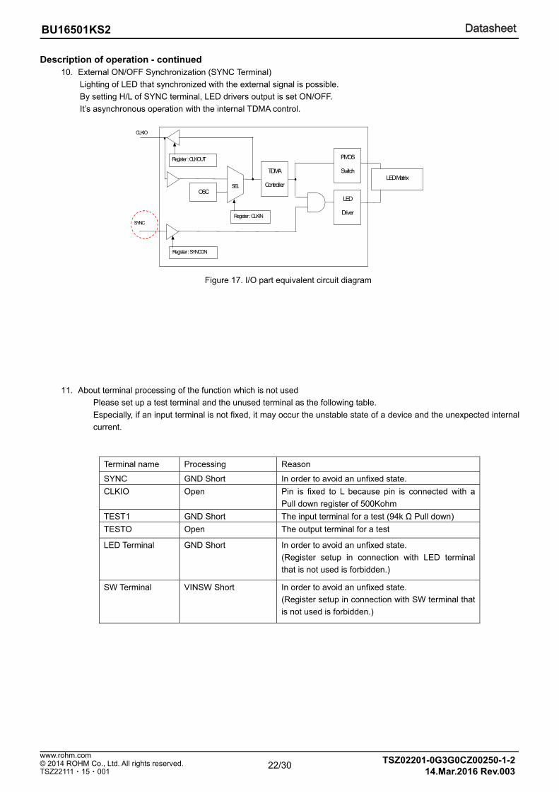
Description of operation - continued 8. I/O
When the RESETB pin is Low, the input buffers (SDA and SCL) are disabling for the Low consumption power.
Figure 14. Input disabling by RESETB
9. Standard Clock Input and Output It is possible to carry out synchronous operation of two or more ICs using the input-and-output function of a standard clock.
Figure 15. I/O part equivalent circuit diagram
・When a clock is supplied from the exterior
Inputting an external standard clock from CLKIN and setting register CLKIN=1, IC operates with the clock inputted from CLKIN as a standard clock.
・When the built-in oscillation circuit of one IC is used
When a clock cannot be supplied from the exterior, it is possible to synchronize between ICs by the connection as the following figure.
Figure 16. It is an example of application for the usage of two or more.
SEL
Register : CLKOUT
SYNC
CLKIO
Register: SYNCON
Register : CLKIN
TDMA
ControllerOSC
PMOS
Switch
LED
Driver
LED Matrix
Level Shift
VBAT
SCL (SDA)
RESETB
LOGIC
VIO
EN
RESETB=L, Output “H”
OSC
CLKIO
IC1
OSC
CLKIO
IC2
OSC
CLKIO
IC3
When a clock supplied from IC1
22/30
DatasheetDatasheetBU16501KS2
© 2014 ROHM Co., Ltd. All rights reserved. www.rohm.com
TSZ22111・15・001
TSZ02201-0G3G0CZ00250-1-214.Mar.2016 Rev.003
Description of operation - continued
10. External ON/OFF Synchronization (SYNC Terminal)
Lighting of LED that synchronized with the external signal is possible.
By setting H/L of SYNC terminal, LED drivers output is set ON/OFF.
It’s asynchronous operation with the internal TDMA control.
Figure 17. I/O part equivalent circuit diagram
11. About terminal processing of the function which is not used
Please set up a test terminal and the unused terminal as the following table.
Especially, if an input terminal is not fixed, it may occur the unstable state of a device and the unexpected internal
current.
Terminal name Processing Reason
SYNC GND Short In order to avoid an unfixed state.
CLKIO Open Pin is fixed to L because pin is connected with a
Pull down register of 500Kohm
TEST1 GND Short The input terminal for a test (94k Ω Pull down)
TESTO Open The output terminal for a test
LED Terminal GND Short In order to avoid an unfixed state.
(Register setup in connection with LED terminal
that is not used is forbidden.)
SW Terminal VINSW Short In order to avoid an unfixed state.
(Register setup in connection with SW terminal that
is not used is forbidden.)
SEL
Register : CLKOUT
SYNC
CLKIO
Register : SYNCON
Register : CLKIN
TDMA
ControllerOSC
PMOS
Switch
LED
Driver
LED Matrix

23/30
DatasheetDatasheetBU16501KS2
© 2014 ROHM Co., Ltd. All rights reserved. www.rohm.com
TSZ22111・15・001
TSZ02201-0G3G0CZ00250-1-214.Mar.2016 Rev.003
Description of operation - continued 12. Setting about VINSW
VINSW is Power Supply about LED Current. It needs proper Voltage range of LED terminal to get proper LED Current
(refer to Page5). If it needs the voltage range, it needs to set up proper Voltage range of VINSW which is Power Supply
about LED.
Figure 18. Set up VINSW Figure 19. SW timing and IOUT
VINSW’s Voltage range is made by V1, V2, V3. (refer to Figure 18)
VINSW_max = V1_min + V2_min + V3_max
VINSW_min = V1_max + V2_max + V3_min
V1:IR Drop Voltage
V1 is IR Voltage drop by SW’s Resistor at ON and IOUT which is the sum of every LED Current. It is V1’s maximum
and minimum that it multiplies by SW’s Resistor at ON and IOUT maximum and minimum in each SW timing. Please
estimate IOUT by setting application. (refer to figure 19). Please refer to page 5 about SW’s Resistor at ON. (And it
needs to estimate parasitic resistor on PCB’s current route).
V1_max = Ron * Iout_max
V1_min = Ron * Iout_min V2: LED Vf V2 is the Voltage drop by LED’s Vf. Please confirm about all LED’s Vf. V2_max = Vf_max V2_min = Vf_min V3: Terminal Voltage to operate
V3 is the terminal Voltage to operate LED Current. (refer to page 5). The minimum is made by IC’s ability. The
maximum is made by VBAT’s minimum in Voltage range. V3_max = VBAT_min – 1.4V V3_min = 0.2V
--Example of Setting VINSW—
Condition: VBAT=3.2 – 4.0 V, Iout_max = 100mA, Iout_min = 20mA, Vf_max = 3.0V, Vf_min = 2.5V
V1_max = 1 ohm * 100mA = 0.1V V1_min = 1 ohm * 20mA = 0.02V
V2_max = 3.0V V2_min = 2.5V
V3_max = 3.2V – 1.4V = 1.8V V3_min = 0.2V
VINSW_max = 0.02V + 2.5V + 1.8V = 4.32V
VINSW_min = 0.1V + 3.0V + 0.2V =3.3V
This is proper Voltage range about VINSW.
SW
LED1
VINSW
V1: IR Drop Voltage
V3: Terminal Voltage to operate
V2: LED Vf
IOUT
LED16
Internal IC External IC
VINSW = V1 + V2 + V3
SW1
SW2
SW3
SW4
SW5
IOUT mA
on/off
on/off
on/off
on/off
on/off
(unit)
Iout_max Iout_min time
IOUT = ILED1 + ILED2 + ************** + ILED16

24/30
DatasheetDatasheetBU16501KS2
© 2014 ROHM Co., Ltd. All rights reserved. www.rohm.com
TSZ22111・15・001
TSZ02201-0G3G0CZ00250-1-214.Mar.2016 Rev.003
Power dissipation (On the ROHM’s standard one layer board)
Figure 20. Power dissipation <Calculator>
Pd=(VINSW-Vf) x ILED x N(Channel) ex ) VINSW=5V, Vf=3.2V, ILED =20mA,N=16channel, Pd =(5-3.2) x 20 x 16=576mW Please adjust VINSW and ILED in order to prevent Pd from exceeding 1300mV of power dissipation. *VINSW: VINSW input voltage *Vf: Diode Vf *ILED: LED Current *N(Channel): LED Channel
0.0
0.2
0.4
0.6
0.8
1.0
1.2
1.4
1.6
1.8
0 25 50 75 100 125 150
Pow
er
Dis
sipa
tion P
d (
W)
Ta()
1300mW

25/30
DatasheetDatasheetBU16501KS2
© 2014 ROHM Co., Ltd. All rights reserved. www.rohm.com
TSZ22111・15・001
TSZ02201-0G3G0CZ00250-1-214.Mar.2016 Rev.003
Operational Notes
1. Reverse Connection of Power Supply Connecting the power supply in reverse polarity can damage the IC. Take precautions against reverse polarity when connecting the power supply, such as mounting an external diode between the power supply and the IC’s power supply pins.
2. Power Supply Lines Design the PCB layout pattern to provide low impedance supply lines. Separate the ground and supply lines of the digital and analog blocks to prevent noise in the ground and supply lines of the digital block from affecting the analog block. Furthermore, connect a capacitor to ground at all power supply pins. Consider the effect of temperature and aging on the capacitance value when using electrolytic capacitors.
3. Ground Voltage Ensure that no pins are at a voltage below that of the ground pin at any time, even during transient condition.
4. Ground Wiring Pattern
When using both small-signal and large-current ground traces, the two ground traces should be routed separately but connected to a single ground at the reference point of the application board to avoid fluctuations in the small-signal ground caused by large currents. Also ensure that the ground traces of external components do not cause variations on the ground voltage. The ground lines must be as short and thick as possible to reduce line impedance.
5. Thermal Consideration
Should by any chance the power dissipation rating be exceeded the rise in temperature of the chip may result in
deterioration of the properties of the chip. The absolute maximum rating of the Pd stated in this specification is when
the IC is mounted on a 70mm x 70mm x 1.6mm glass epoxy board. In case of exceeding this absolute maximum
rating, increase the board size and copper area to prevent exceeding the Pd rating.
6. Recommended Operating Conditions These conditions represent a range within which the expected characteristics of the IC can be approximately obtained. The electrical characteristics are guaranteed under the conditions of each parameter.
7. Inrush Current
When power is first supplied to the IC, it is possible that the internal logic may be unstable and inrush current may flow instantaneously due to the internal powering sequence and delays, especially if the IC has more than one power supply. Therefore, give special consideration to power coupling capacitance, power wiring, width of ground wiring, and routing of connections.
8. Operation Under Strong Electromagnetic Field
Operating the IC in the presence of a strong electromagnetic field may cause the IC to malfunction.
9. Testing on Application Boards When testing the IC on an application board, connecting a capacitor directly to a low-impedance output pin may subject the IC to stress. Always discharge capacitors completely after each process or step. The IC’s power supply should always be turned off completely before connecting or removing it from the test setup during the inspection process. To prevent damage from static discharge, ground the IC during assembly and use similar precautions during transport and storage.
10. Inter-pin Short and Mounting Errors Ensure that the direction and position are correct when mounting the IC on the PCB. Incorrect mounting may result in damaging the IC. Avoid nearby pins being shorted to each other especially to ground, power supply and output pin. Inter-pin shorts could be due to many reasons such as metal particles, water droplets (in very humid environment) and unintentional solder bridge deposited in between pins during assembly to name a few.

26/30
DatasheetDatasheetBU16501KS2
© 2014 ROHM Co., Ltd. All rights reserved. www.rohm.com
TSZ22111・15・001
TSZ02201-0G3G0CZ00250-1-214.Mar.2016 Rev.003
Operational Notes – continued 11. Unused Input Pins
Input pins of an IC are often connected to the gate of a MOS transistor. The gate has extremely high impedance and extremely low capacitance. If left unconnected, the electric field from the outside can easily charge it. The small charge acquired in this way is enough to produce a significant effect on the conduction through the transistor and cause unexpected operation of the IC. So unless otherwise specified, unused input pins should be connected to the power supply or ground line.
12. Regarding the Input Pin of the IC
This monolithic IC contains P+ isolation and P substrate layers between adjacent elements in order to keep them isolated. P-N junctions are formed at the intersection of the P layers with the N layers of other elements, creating a parasitic diode or transistor. For example (refer to figure below):
When GND > Pin A and GND > Pin B, the P-N junction operates as a parasitic diode. When GND > Pin B, the P-N junction operates as a parasitic transistor.
Parasitic diodes inevitably occur in the structure of the IC. The operation of parasitic diodes can result in mutual interference among circuits, operational faults, or physical damage. Therefore, conditions that cause these diodes to operate, such as applying a voltage lower than the GND voltage to an input pin (and thus to the P substrate) should be avoided.
Figure 20. Example of monolithic IC structure
13. Ceramic Capacitor When using a ceramic capacitor, determine the dielectric constant considering the change of capacitance with temperature and the decrease in nominal capacitance due to DC bias and others.
14. Area of Safe Operation (ASO)
Operate the IC such that the output voltage, output current, and power dissipation are all within the Area of Safe Operation (ASO).
15. Thermal Shutdown Circuit(TSD)
This IC has a built-in thermal shutdown circuit that prevents heat damage to the IC. Normal operation should always be within the IC’s power dissipation rating. If however the rating is exceeded for a continued period, the junction temperature (Tj) will rise which will activate the TSD circuit that will turn OFF all output pins. When the Tj falls below the TSD threshold, the circuits are automatically restored to normal operation. Note that the TSD circuit operates in a situation that exceeds the absolute maximum ratings and therefore, under no circumstances, should the TSD circuit be used in a set design or for any purpose other than protecting the IC from heat damage.
16. Over Current Protection Circuit (OCP) This IC incorporates an integrated overcurrent protection circuit that is activated when the load is shorted. This protection circuit is effective in preventing damage due to sudden and unexpected incidents. However, the IC should not be used in applications characterized by continuous operation or transitioning of the protection circuit.
17. Disturbance light In a device where a portion of silicon is exposed to light such as in a WL-CSP, IC characteristics may be affected due to photoelectric effect. For this reason, it is recommended to come up with countermeasures that will prevent the chip from being exposed to light.

27/30
DatasheetDatasheetBU16501KS2
© 2014 ROHM Co., Ltd. All rights reserved. www.rohm.com
TSZ22111・15・001
TSZ02201-0G3G0CZ00250-1-214.Mar.2016 Rev.003
Ordering Information
B U 1 6 5 0 1 K S 2 - E 2
Part Number
Package KS2: SQFP-T52M SQFP-T52
Packaging and forming specification E2: Embossed tape and reel
Marking Diagram
Marking Package Wire
BU16501GD SQFP-T52M SQFP-T52
Au
BU16501KS2 SQFP-T52 Cu
(TOP VIEW)
BU16501GD
Part Number Marking
LOT Number
1PIN MARK
(TOP VIEW)
BU16501KS2
Part Number Marking
LOT Number
1PIN MARK

28/30
DatasheetDatasheetBU16501KS2
© 2014 ROHM Co., Ltd. All rights reserved. www.rohm.com
TSZ22111・15・001
TSZ02201-0G3G0CZ00250-1-214.Mar.2016 Rev.003
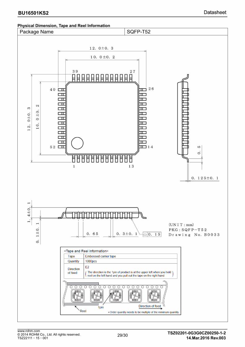
Physical Dimensions Tape and Reel Information
Package Name SQFP-T52M
29/30
DatasheetDatasheetBU16501KS2
© 2014 ROHM Co., Ltd. All rights reserved. www.rohm.com
TSZ22111・15・001
TSZ02201-0G3G0CZ00250-1-214.Mar.2016 Rev.003
Physical Dimension, Tape and Reel Information
Package Name SQFP-T52
30/30
DatasheetDatasheetBU16501KS2
© 2014 ROHM Co., Ltd. All rights reserved. www.rohm.com
TSZ22111・15・001
TSZ02201-0G3G0CZ00250-1-214.Mar.2016 Rev.003
Revision History
Date Revision Changes
01.Oct.2013 001 New Release
04.Sep.2014 002 Additional SQFP-T52 package and marking image
14.Mar.2016 003 Modified the marking

Notice-PGA-E Rev.003
© 2015 ROHM Co., Ltd. All rights reserved.
Notice
Precaution on using ROHM Products 1. Our Products are designed and manufactured for application in ordinary electronic equipments (such as AV equipment,
OA equipment, telecommunication equipment, home electronic appliances, amusement equipment, etc.). If you intend to use our Products in devices requiring extremely high reliability (such as medical equipment
(Note 1), transport
equipment, traffic equipment, aircraft/spacecraft, nuclear power controllers, fuel controllers, car equipment including car accessories, safety devices, etc.) and whose malfunction or failure may cause loss of human life, bodily injury or serious damage to property (“Specific Applications”), please consult with the ROHM sales representative in advance. Unless otherwise agreed in writing by ROHM in advance, ROHM shall not be in any way responsible or liable for any damages, expenses or losses incurred by you or third parties arising from the use of any ROHM’s Products for Specific Applications.
(Note1) Medical Equipment Classification of the Specific Applications
JAPAN USA EU CHINA
CLASSⅢ CLASSⅢ
CLASSⅡb CLASSⅢ
CLASSⅣ CLASSⅢ
2. ROHM designs and manufactures its Products subject to strict quality control system. However, semiconductor
products can fail or malfunction at a certain rate. Please be sure to implement, at your own responsibilities, adequate safety measures including but not limited to fail-safe design against the physical injury, damage to any property, which a failure or malfunction of our Products may cause. The following are examples of safety measures:
[a] Installation of protection circuits or other protective devices to improve system safety [b] Installation of redundant circuits to reduce the impact of single or multiple circuit failure
3. Our Products are designed and manufactured for use under standard conditions and not under any special or extraordinary environments or conditions, as exemplified below. Accordingly, ROHM shall not be in any way responsible or liable for any damages, expenses or losses arising from the use of any ROHM’s Products under any special or extraordinary environments or conditions. If you intend to use our Products under any special or extraordinary environments or conditions (as exemplified below), your independent verification and confirmation of product performance, reliability, etc, prior to use, must be necessary:
[a] Use of our Products in any types of liquid, including water, oils, chemicals, and organic solvents [b] Use of our Products outdoors or in places where the Products are exposed to direct sunlight or dust [c] Use of our Products in places where the Products are exposed to sea wind or corrosive gases, including Cl2,
H2S, NH3, SO2, and NO2
[d] Use of our Products in places where the Products are exposed to static electricity or electromagnetic waves [e] Use of our Products in proximity to heat-producing components, plastic cords, or other flammable items [f] Sealing or coating our Products with resin or other coating materials [g] Use of our Products without cleaning residue of flux (even if you use no-clean type fluxes, cleaning residue of
flux is recommended); or Washing our Products by using water or water-soluble cleaning agents for cleaning residue after soldering
[h] Use of the Products in places subject to dew condensation
4. The Products are not subject to radiation-proof design. 5. Please verify and confirm characteristics of the final or mounted products in using the Products. 6. In particular, if a transient load (a large amount of load applied in a short period of time, such as pulse. is applied,
confirmation of performance characteristics after on-board mounting is strongly recommended. Avoid applying power exceeding normal rated power; exceeding the power rating under steady-state loading condition may negatively affect product performance and reliability.
7. De-rate Power Dissipation depending on ambient temperature. When used in sealed area, confirm that it is the use in
the range that does not exceed the maximum junction temperature. 8. Confirm that operation temperature is within the specified range described in the product specification. 9. ROHM shall not be in any way responsible or liable for failure induced under deviant condition from what is defined in
this document.
Precaution for Mounting / Circuit board design 1. When a highly active halogenous (chlorine, bromine, etc.) flux is used, the residue of flux may negatively affect product
performance and reliability.
2. In principle, the reflow soldering method must be used on a surface-mount products, the flow soldering method must be used on a through hole mount products. If the flow soldering method is preferred on a surface-mount products, please consult with the ROHM representative in advance.
For details, please refer to ROHM Mounting specification

Notice-PGA-E Rev.003
© 2015 ROHM Co., Ltd. All rights reserved.
Precautions Regarding Application Examples and External Circuits 1. If change is made to the constant of an external circuit, please allow a sufficient margin considering variations of the
characteristics of the Products and external components, including transient characteristics, as well as static characteristics.
2. You agree that application notes, reference designs, and associated data and information contained in this document
are presented only as guidance for Products use. Therefore, in case you use such information, you are solely responsible for it and you must exercise your own independent verification and judgment in the use of such information contained in this document. ROHM shall not be in any way responsible or liable for any damages, expenses or losses incurred by you or third parties arising from the use of such information.
Precaution for Electrostatic This Product is electrostatic sensitive product, which may be damaged due to electrostatic discharge. Please take proper caution in your manufacturing process and storage so that voltage exceeding the Products maximum rating will not be applied to Products. Please take special care under dry condition (e.g. Grounding of human body / equipment / solder iron, isolation from charged objects, setting of Ionizer, friction prevention and temperature / humidity control).
Precaution for Storage / Transportation 1. Product performance and soldered connections may deteriorate if the Products are stored in the places where:
[a] the Products are exposed to sea winds or corrosive gases, including Cl2, H2S, NH3, SO2, and NO2 [b] the temperature or humidity exceeds those recommended by ROHM [c] the Products are exposed to direct sunshine or condensation [d] the Products are exposed to high Electrostatic
2. Even under ROHM recommended storage condition, solderability of products out of recommended storage time period may be degraded. It is strongly recommended to confirm solderability before using Products of which storage time is exceeding the recommended storage time period.
3. Store / transport cartons in the correct direction, which is indicated on a carton with a symbol. Otherwise bent leads
may occur due to excessive stress applied when dropping of a carton. 4. Use Products within the specified time after opening a humidity barrier bag. Baking is required before using Products of
which storage time is exceeding the recommended storage time period.
Precaution for Product Label A two-dimensional barcode printed on ROHM Products label is for ROHM’s internal use only.
Precaution for Disposition When disposing Products please dispose them properly using an authorized industry waste company.
Precaution for Foreign Exchange and Foreign Trade act Since concerned goods might be fallen under listed items of export control prescribed by Foreign exchange and Foreign trade act, please consult with ROHM in case of export.
Precaution Regarding Intellectual Property Rights 1. All information and data including but not limited to application example contained in this document is for reference
only. ROHM does not warrant that foregoing information or data will not infringe any intellectual property rights or any other rights of any third party regarding such information or data.
2. ROHM shall not have any obligations where the claims, actions or demands arising from the combination of the Products with other articles such as components, circuits, systems or external equipment (including software).
3. No license, expressly or implied, is granted hereby under any intellectual property rights or other rights of ROHM or any third parties with respect to the Products or the information contained in this document. Provided, however, that ROHM will not assert its intellectual property rights or other rights against you or your customers to the extent necessary to manufacture or sell products containing the Products, subject to the terms and conditions herein.
Other Precaution 1. This document may not be reprinted or reproduced, in whole or in part, without prior written consent of ROHM.
2. The Products may not be disassembled, converted, modified, reproduced or otherwise changed without prior written consent of ROHM.
3. In no event shall you use in any way whatsoever the Products and the related technical information contained in the Products or this document for any military purposes, including but not limited to, the development of mass-destruction weapons.
4. The proper names of companies or products described in this document are trademarks or registered trademarks of ROHM, its affiliated companies or third parties.

DatasheetDatasheet
Notice – WE Rev.001© 2015 ROHM Co., Ltd. All rights reserved.
General Precaution 1. Before you use our Pro ducts, you are requested to care fully read this document and fully understand its contents.
ROHM shall n ot be in an y way responsible or liabl e for fa ilure, malfunction or acci dent arising from the use of a ny ROHM’s Products against warning, caution or note contained in this document.
2. All information contained in this docume nt is current as of the issuing date and subj ect to change without any prior
notice. Before purchasing or using ROHM’s Products, please confirm the la test information with a ROHM sale s representative.
3. The information contained in this doc ument is provi ded on an “as is” basis and ROHM does not warrant that all
information contained in this document is accurate an d/or error-free. ROHM shall not be in an y way responsible or liable for any damages, expenses or losses incurred by you or third parties resulting from inaccuracy or errors of or concerning such information.