Wafer Level Fabrication of Nanowell Array Biochip and Its ...€¦ · Wafer Level Fabrication of...
24
October 15, 2013 Wafer Level Fabrication of Nanowell Array Biochip and Its Characterization Jin-Goo Park Department of Materials Engineering, Hanyang University, Ansan, 426-791, Korea The Tenth U.S.-Korea Forum on Nanotechnology, Boston
Transcript of Wafer Level Fabrication of Nanowell Array Biochip and Its ...€¦ · Wafer Level Fabrication of...

October 15, 2013
Wafer Level Fabrication of Nanowell Array Biochip and Its Characterization
Jin-Goo Park
Department of Materials Engineering, Hanyang University,Ansan, 426-791, Korea
The Tenth U.S.-Korea Forum on Nanotechnology, Boston

2 Nano-Bio Electronic Materials and Processing Lab.
Acknowledgements
Funding from KRF Center for Human Sensing Systems (ERC) at Hanyang University.
Funding from BK21 Plus Program for Bio Nano Technology at Hanyang University.
Prof. H. Y. Lee of Northeastern University for biochip design and characterization
Seongpil Hwang et,al., Chemworld (2010) 05, 25--28

3 Nano-Bio Electronic Materials and Processing Lab.
Summary
Development and Characterization
Introduction- Nano Array Biochip- Advantages of nanowell array biochip- Conventional manufacturing methods
- Development of fabricating nanowell array biochip- Characterization of fabricated nanowell array biochip
Contents

4 Nano-Bio Electronic Materials and Processing Lab.
Why nanowell array (NWA) biochip?
- Rapid response time (small RC delay)- Small iR drop (reduction of noise and Increased sensitivity)- High mass-transport rate leading to steady-state diffusion (high S/N),
Enhanced faradic currents (radial diffusion)- Highly sensitive and specific biomolecular assay with a small amount
[Ref.] D. Wei et. al., Lab Chip, 9 (2009) pp. 2123-2131
[Ref.] H.Y.Lee,T.Kawai et, al., Langmuir 21, p.6025-6029 (2005).

5 Nano-Bio Electronic Materials and Processing Lab.
- Higher mass transfer rates in micro/nanoelectrode due to radial diffusion- Bulk electrode that operate via planar diffusion
Phenomenon at Nanowell Electrode
Nano electrode Micro electrode Bulk electrode
S. Hwang et,al., Chemworld (2010) 05, 25--28
[Ref.] J. C. Hulteen et .al., J. Chem. Soc., Faraday Trans. 92 (1996) 4029T. J. Davies and R. G. Compton, J. Electroanal. Chem. 585 (2005) 63

6 Nano-Bio Electronic Materials and Processing Lab.
Reported fabrication methods of NWA biochip
Jung et al. Langmuir 21, 6025-6029 (2005)- Method : E-beam lithography- Limitation : Small area, Low throughput
Kim P. et al. Adv. Mater. 20, 31-36 (2008)- Method : Soft lithography with PUA mold- Limitation : Small area, Low reliability
Lee et al. Anal. Chem. 83, 9174-9180 (2011)- Method : Colloidal lithography (CL)- Limitation : Non-uniform nanoarray structure
Lee et al. Lab Chip 9, 132-139 (2009)- Method : UV nanoimprinting (UV-NIL)- Limitation : Costly mold, Low repeatability

7 Nano-Bio Electronic Materials and Processing Lab.
Research Motivation
Fabrication of highly sensitive biochip based on nanowell array (NWA)
Development of manufacturing process for mass production
Characterization of NWA biochip using electrochemical analysis
Nano well array device Electrochemical Sensing System

8 Nano-Bio Electronic Materials and Processing Lab.
Nano Array Biochips
By geometries of electrodes By position of electrodes
(a) Inlaid electrodes
(b) Recessed electrodes
In this study, nanowell array (NWA) Nanoelectrode arrays (NEAs) and recessed type
[Ref.] C. G. Zoski, Electroanalysis, 14 (2002) pp. 1041-1051

9 Nano-Bio Electronic Materials and Processing Lab.
Fabrication Process of NWA Biochip
Process Procedure (Vertical view)
[Ref.] M. S. Cha et. al., J. Nanosci. Nanotechnol. 13 (2013) pp. 5245 -5249J. K. Lee et. al., J. Biotechnology (2013) In Press
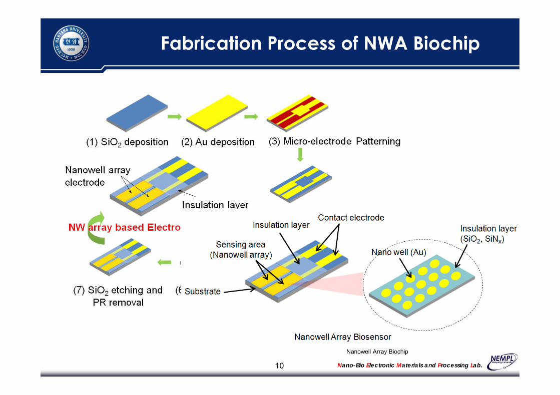
10 Nano-Bio Electronic Materials and Processing Lab.
Fabrication Process of NWA Biochip
Nanowell Array Biochip

11 Nano-Bio Electronic Materials and Processing Lab.
Fabricated NWA Biochip
Mass production of NWA chips
Chip size (1ea) : 21.215 x 9.78 mm2 , Electrode area = 4 x 2 mm2

12 Nano-Bio Electronic Materials and Processing Lab.
Fabricated NWA Biochip
(d) Bare Au Chip
FE-SEM & EDS result
(a, b, c) FE-SEM image of nanowell array structure (d) EDS result

13 Nano-Bio Electronic Materials and Processing Lab.
Topography (5 μm2)
Current AFM image (5 μm2)
AFM conditions
AFM Tip InformationModel Name : PPP-CONTSCPTManufacturer : Nanosensors
Point Probe Plus Contact Mode Short Cantilever PtIr5 Coating
I-AFM Result of SiO2 NWA chip

14 Nano-Bio Electronic Materials and Processing Lab.
I-AFM Result of Bare Au chip
Topography (5 μm2)
Current AFM image (5 μm2)
AFM conditions
AFM Tip InformationModel Name : PPP-CONTSCPTManufacturer : Nanosensors
Point Probe Plus Contact Mode Short Cantilever PtIr5 Coating

15 Nano-Bio Electronic Materials and Processing Lab.
Preparation of Immuno-affinity layer
• Self-Assembled Monolayer (SAM) on a nanowell(NW) electrode: incubating 10 mM, 11-mercaptoundecanoic acid (11-MUA) in anhydrous ethanol for 1 hour at room temperature (linker)
• The formation of active ester functional group : 50 mM EDC and 50 mM NHS in pH 5.5 sodium acetate buffer treatment
• Immobilization: Streptavidin 1 mg/ml in PBS for 30 min at room temperature,
10 μg/ml biotinylated antibody immobilized on electrode• Antigen (Target material)
: Stress-induced-phosphoprotein-1 (STIP-1), Biomarker of Ovarian Cancer

16 Nano-Bio Electronic Materials and Processing Lab.
Schematic of Immuno-affinity layer

17 Nano-Bio Electronic Materials and Processing Lab.
Electrochemical characterization (1)
(a) Nyquist plot from EIS (b) Cyclic voltammogram
0 5 10 15 20 25 30 35 40 450
-5
-10
-15
-20
-25
-30
-35
-40
-45
Z'' (
kohm
)
Z' (kohm)
NW electrode Bare electrode
-400 -200 0 200 400 600 800
-35-30-25-20-15-10-505
10152025
Q : 14.88 mC
Cur
rent
(uA
)
Potential vs Ag/AgCl (mV)
NW electrode Bare electrode
Q : 27.05 mC
The Rct of NW electrode is 20.87 kohm and bare electrode is 42.98 kohm. NW electrode has higher current and lower charge transfer resistance than bare. The electrons in NW’s double layer easily pass from electrode to solution than bare.
Electron transfer imaging using EIS and CV of Nanowell and Bare electrode
[Ref.] J. K. Lee et. al., J. Biotechnology (2013) In Press

18 Nano-Bio Electronic Materials and Processing Lab.
Electrochemical characterization (2)
Impedance measurement of Nanowell and Bare electrode
0 10 20 30 40 50 60 70 80 90 1000
-5
-10
-15
-20
-25
-30
-35
-40
Z'' (
kohm
)
Z' (kohm)
Base 10 pg/ml 100 pg/ml 1 ng/ml 10 ng/ml 100 ng/ml 1000 ng/ml
0 10 20 30 40 50 60 700
-5
-10
-15
-20
-25
-30
-35
-40
Base 10 pg/ml 100 pg/ml 1 ng/ml 10 ng/ml 100 ng/ml 1000 ng/ml
Z'' (
kohm
)
Z' (kohm)(a) Nanowell electrode (b) Bare electrode
After treatment of streptavidin and biotinlylated antibody (base), then we treated antigen changing with its concentration. (10 pg/ml ~ 1000 ng/ml)
The base signal of bare electrode is 52 kohm that is 43 % increased compare with the base signal (37 kohm) of NW electrode.
The Rct of NW electrode with the increase of antigen increased very evidently. The differences at bare electrode are smaller than differences at NW electrode.

19 Nano-Bio Electronic Materials and Processing Lab.
Electrochemical characterization (3)
Limit of detection (LOD) estimation from standard curve
0.01 0.1 1 10 100 1000-5
0
5
10
15
20
25
30
35
40
45 NW's electrode NW's electrode (w/o antibody) Bare electrode
R
ct (k
ohm
)
[Antigen] (ng/ml) The movement of Rct by changing antigen concentration was showed. The signal at low concentration in bare electrode interferes. This indicates
low SNR because of non-specific binding. At NW electrode, LOD was estimated to be approximately 10 pg/ml, which is
more than 100-fold improved LOD in comparion to the bare electrode. NW electrode has high sensitivity, selectivity and very low LOD.
[Ref.] J. K. Lee et. al., J. Biotechnology (2013) In Press
20 Nano-Bio Electronic Materials and Processing Lab.
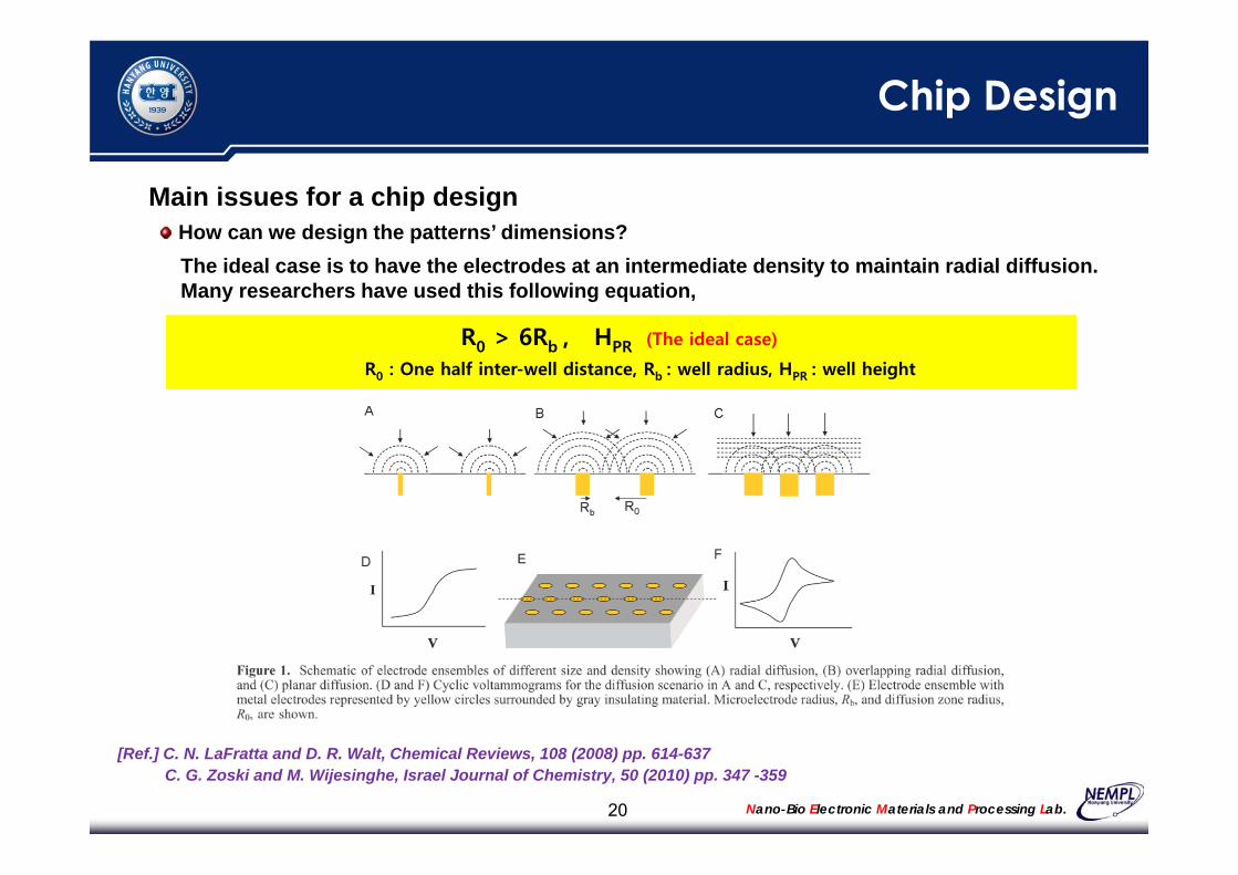
Chip Design
How can we design the patterns’ dimensions?Main issues for a chip design
R0 > 6Rb , HPR (The ideal case)
R0 : One half inter-well distance, Rb : well radius, HPR : well height
[Ref.] C. N. LaFratta and D. R. Walt, Chemical Reviews, 108 (2008) pp. 614-637C. G. Zoski and M. Wijesinghe, Israel Journal of Chemistry, 50 (2010) pp. 347 -359
The ideal case is to have the electrodes at an intermediate density to maintain radial diffusion.Many researchers have used this following equation,

21 Nano-Bio Electronic Materials and Processing Lab.
Modeling for Simulation
Fig. 2. 2D model of diffusion domain of nanowell and examples of simulation result
Table 1. Simulation geometries of various cases of nanowell array chip
*Cell height, , tmax : the time for ½ CV scan, D : diffusion coefficient
Case Rb (μm) R0 (μm) Spacing (μm) C To C (μm) Hpr (μm) Zmax (μm) Scan rate (v/s)
1 0.25 0.5 0.5 1 0.2
245 0.1
2 0.25 1.5 2.5 3 0.23 0.25 2.5 4.5 5 0.24 0.25 0.5 0.5 1 0.55 0.25 1.5 2.5 3 0.56 0.25 2.5 4.5 5 0.5
COMSOL Multiphysics® Modeling (Ver. 4.3)

22 Nano-Bio Electronic Materials and Processing Lab.
Simulation Results
-0.6 -0.4 -0.2 0.0 0.2 0.4 0.6-2.0
-1.5
-1.0
-0.5
0.0
0.5
1.0
1.5
2.0
2.5
3.0
Cur
rent
(A)
Potential (V)
Rb=0.25, R0=0.5, H=0.2 Rb=0.25, R0=1.5, H=0.2 Rb=0.25, R0=2.5, H=0.2
*Unit = um
x10-12
-0.6 -0.4 -0.2 0.0 0.2 0.4 0.6
-1.0
-0.5
0.0
0.5
1.0
1.5
2.0
Cur
rent
(A)
Potential (V)
Rb=0.25, R0=0.5, H=0.5 Rb=0.25, R0=1.5, H=0.5 Rb=0.25, R0=2.5, H=0.5
*Unit = um
x10-12
Cyclic voltammograms as a function of different R0 (1/2 Interwell spacing)
The NWA chip becomes more effective when R0 value is larger and the height of nanowell is smaller.
The simulation study will be continuously performed for the more understanding of nanowell array chip.

23 Nano-Bio Electronic Materials and Processing Lab.
Summary
Seongpil Hwang et,al., Chemworld (2010) 05, 25--28
A highly sensitive biochip was developed by using nanowell
array electrode structure.
The fabrication process was developed for mass production of
nanowell array biochip.
Materials and design optimization needed for future study

24 Nano-Bio Electronic Materials and Processing Lab.