
Wafer-scale micro-optics fabrication · 2017-05-17 · Wafer-scale micro-optics fabrication is...
16
Adv. Opt. Techn., Vol. 1 (2012), pp. 135–150 • Copyright © 2012 THOSS Media and De Gruyter. DOI 10.1515/aot-2012-0013 www.degruyter.com/aot Review Article Wafer-scale micro-optics fabrication Reinhard Voelkel SUSS MicroOpticsSA, Jaquet-Droz 7, CH-2000 Neuchâtel, Switzerland e-mail: [email protected] Received April 12, 2012; accepted May 23, 2012 Abstract Micro-optics is an indispensable key enabling technology for many products and applications today. Probably the most prestigious examples are the diffractive light shaping elements used in high-end DUV lithography steppers. Highly-efficient refractive and diffractive micro-optical elements are used for precise beam and pupil shaping. Micro-optics had a major impact on the reduction of aberrations and diffraction effects in projection lithography, allowing a resolution enhancement from 250 nm to 45 nm within the past decade. Micro-optics also plays a decisive role in medical devices (endoscopes, ophthalmology), in all laser-based devices and fiber com- munication networks, bringing high-speed internet to our homes. Even our modern smart phones contain a variety of micro-optical elements. For example, LED flash light shaping elements, the secondary camera, ambient light and proxim- ity sensors. Wherever light is involved, micro-optics offers the chance to further miniaturize a device, to improve its per- formance, or to reduce manufacturing and packaging costs. Wafer-scale micro-optics fabrication is based on technology established by the semiconductor industry. Thousands of components are fabricated in parallel on a wafer. This review paper recapitulates major steps and inventions in wafer-scale micro-optics technology. The state-of-the-art of fabrication, testing and packaging technology is summarized. Keywords: beam shaping; confocal microscope; diffractive optical elements; fiber coupling; microlens array; micro- optics; wafer-level optics; wafer-level packaging. 1. Miniaturized lenses and array optics The first micro-optical elements were manufactured by Antonie van Leeuwenhoek (1632–1723), a pioneer of micros- copy and microbiology. Leeuwenhoek melted small rods of soda lime glass in a hot flame to obtain high-quality glass spheres. These ball lenses improved the resolution of his microscope viewers beyond current limits. He was the first to observe and report on single cell micro-organisms. Another pioneer of microscopy, Robert Hooke (1635–1703), published his famous book ‘Micrographia’, a collection of microscope observations, in 1665 [1]. Among them is the fascinating drawing of a fly’s compound eye shown in Figure 1, a natural microlens array. The first natural microlens arrays appeared very early in evolution some 500 million years ago, in the Early Cambrian period. Trilobites, a fossil group of marine arthropods, had com- plex compound eyes with microlenses made of calcite (Figure 2). Still today, similar compound eyes are found in many small creatures. Microlens arrays seem to be the appro- priate solution for miniaturized vision systems in nature. 2. Early inventors and microlens arrays The development of planar diffractive and refractive micro- optics is very much connected with photo- and cinematog- raphy. In 1891, Gabriel Lippmann (1845–1921) invented ‘interference color photography’ [2]. He fixed a mirror in contact to the photographic emulsion and recorded the inter- ference pattern from incident and reflected light in a sensi- tive but transparent emulsion. The Lippmann color photos, later referred to as Lippmann holograms, were in fact the first wavelength-selective volume holograms. For white light illu- mination, constructive and destructive interference generated the color image in reflection. This invention was made without laser and long before Denis Gabor invented the holography in 1948 [3]. Lippmann also invented ‘integral photography’, an auto-stereoscopic method to display three-dimensional (3D) images for observation with the naked eye [4]. Integral photography uses an array of small microlenses to record multiple sub-images of a scene in a photographic layer. Each microlens acts like a miniaturized camera recording an individual sub-image. Observing the developed photo plate through a similar lens array, the superimposed sub-images form an auto-stereoscopic integral image, a 3D image. In 1912, Walter Hess [5] proposed to use an array of cylindrical microlenses as shown in Figure 3. These 3D displays based on cylindrical microlens arrays were later referred to as paral- lax panoramagrams. Current 3D postcards and some current 3D television screens are based on this principle. Another important field of applications for microlens arrays include the fly’s eye condensers, also referred to as Köhler integrators, providing a uniform illumination for color slide Brought to you by | European Optical Society (EOS) Authenticated | 172.16.1.226 Download Date | 8/10/12 4:15 PM
Transcript of Wafer-scale micro-optics fabrication · 2017-05-17 · Wafer-scale micro-optics fabrication is...
Adv. Opt. Techn., Vol. 1 (2012), pp. 135–150 • Copyright © 2012 THOSS Media and De Gruyter. DOI 10.1515/aot-2012-0013
www.degruyter.com/aot
Review Article
Wafer-scale micro-optics fabrication
Reinhard Voelkel
SUSS MicroOpticsSA , Jaquet-Droz 7, CH-2000 Neuch â tel , Switzerland
e-mail: [email protected] Received April 12, 2012; accepted May 23, 2012
Abstract
Micro-optics is an indispensable key enabling technology for many products and applications today. Probably the most prestigious examples are the diffractive light shaping elements used in high-end DUV lithography steppers. Highly-effi cient refractive and diffractive micro-optical elements are used for precise beam and pupil shaping. Micro-optics had a major impact on the reduction of aberrations and diffraction effects in projection lithography, allowing a resolution enhancement from 250 nm to 45 nm within the past decade. Micro-optics also plays a decisive role in medical devices (endoscopes, ophthalmology), in all laser-based devices and fi ber com-munication networks, bringing high-speed internet to our homes. Even our modern smart phones contain a variety of micro-optical elements. For example, LED fl ash light shaping elements, the secondary camera, ambient light and proxim-ity sensors. Wherever light is involved, micro-optics offers the chance to further miniaturize a device, to improve its per-formance, or to reduce manufacturing and packaging costs. Wafer-scale micro-optics fabrication is based on technology established by the semiconductor industry. Thousands of components are fabricated in parallel on a wafer. This review paper recapitulates major steps and inventions in wafer-scale micro-optics technology. The state-of-the-art of fabrication, testing and packaging technology is summarized.
Keywords: beam shaping; confocal microscope; diffractive optical elements; fi ber coupling; microlens array; micro-optics; wafer-level optics; wafer-level packaging.
1. Miniaturized lenses and array optics
The fi rst micro-optical elements were manufactured by Antonie van Leeuwenhoek (1632 – 1723), a pioneer of micros-copy and microbiology. Leeuwenhoek melted small rods of soda lime glass in a hot fl ame to obtain high-quality glass
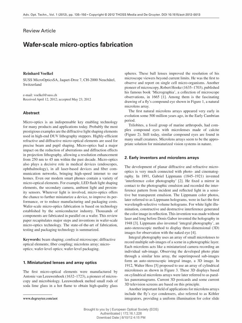
spheres. These ball lenses improved the resolution of his microscope viewers beyond current limits. He was the fi rst to observe and report on single cell micro-organisms. Another pioneer of microscopy, Robert Hooke (1635 – 1703), published his famous book ‘ Micrographia ’ , a collection of microscope observations, in 1665 [1] . Among them is the fascinating drawing of a fl y ’ s compound eye shown in Figure 1 , a natural microlens array.
The fi rst natural microlens arrays appeared very early in evolution some 500 million years ago, in the Early Cambrian period.
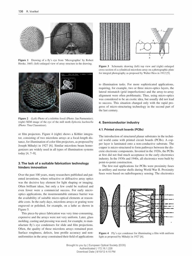
Trilobites, a fossil group of marine arthropods, had com-plex compound eyes with microlenses made of calcite (Figure 2 ). Still today, similar compound eyes are found in many small creatures. Microlens arrays seem to be the appro-priate solution for miniaturized vision systems in nature.
2. Early inventors and microlens arrays
The development of planar diffractive and refractive micro-optics is very much connected with photo- and cinematog-raphy. In 1891, Gabriel Lippmann (1845 – 1921) invented ‘ interference color photography ’ [2] . He fi xed a mirror in contact to the photographic emulsion and recorded the inter-ference pattern from incident and refl ected light in a sensi-tive but transparent emulsion. The Lippmann color photos, later referred to as Lippmann holograms, were in fact the fi rst wavelength-selective volume holograms. For white light illu-mination, constructive and destructive interference generated the color image in refl ection. This invention was made without laser and long before Denis Gabor invented the holography in 1948 [3] . Lippmann also invented ‘ integral photography ’ , an auto-stereoscopic method to display three-dimensional (3D) images for observation with the naked eye [4] .
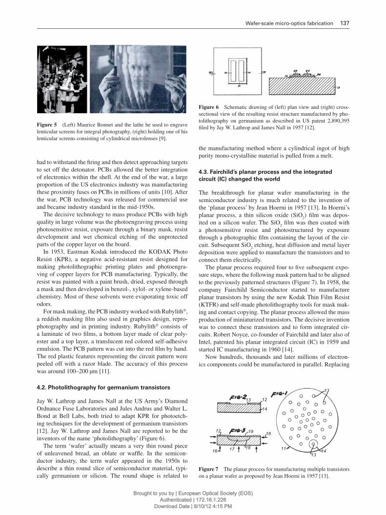
Integral photography uses an array of small microlenses to record multiple sub-images of a scene in a photographic layer. Each microlens acts like a miniaturized camera recording an individual sub-image. Observing the developed photo plate through a similar lens array, the superimposed sub-images form an auto-stereoscopic integral image, a 3D image. In 1912, Walter Hess [5] proposed to use an array of cylindrical microlenses as shown in Figure 3 . These 3D displays based on cylindrical microlens arrays were later referred to as paral-lax panoramagrams. Current 3D postcards and some current 3D television screens are based on this principle.
Another important fi eld of applications for microlens arrays include the fl y ’ s eye condensers, also referred to as K ö hler integrators, providing a uniform illumination for color slide
Brought to you by | European Optical Society (EOS)Authenticated | 172.16.1.226
Download Date | 8/10/12 4:15 PM
136 R. Voelkel
to illumination tasks. For more sophisticated applications, requiring, for example, two or three micro-optics layers, the lateral mismatch (grid imperfections) and the array-to-array alignment were often problematic. Thus, using micro-optics was considered to be an exotic idea, but usually did not lead to success. This situation changed only with the rapid pro-gress of micro-structuring technology in the second part of the last century.
4. Semiconductor industry
4.1. Printed circuit boards (PCBs)
The introduction of structured planar substrates in the techni-cal world came with printed circuit boards (PCBs). A cop-per layer is laminated onto a non-conductive substrate. The copper is micro-structured to form pathways between the dis-crete electronic components. Invented in the 1920s, the PCBs at fi rst did not fi nd much acceptance in the early electronics industry. In the 1930s and 1940s, all electronics were built by point-to-point construction.
The fi rst real applications for PCBs were proximity fuses in artillery and mortar shells during World War II. Proximity fuses were based on radiofrequency sensing. The electronics
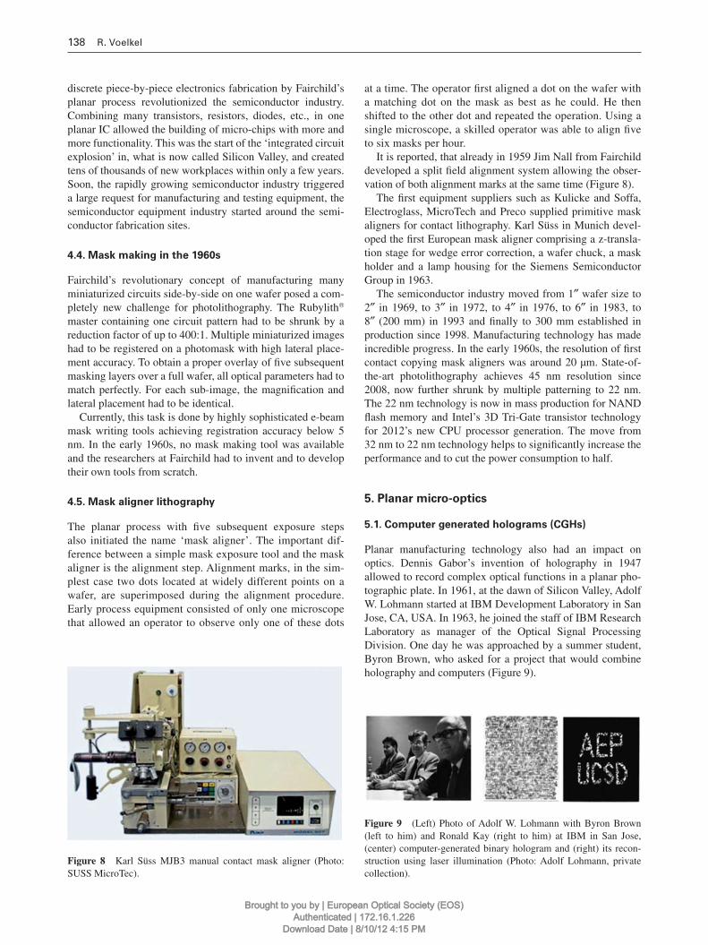
or fi lm projectors. Figure 4 (right) shows a K ö hler integra-tor, consisting of two microlens arrays at a focal-length dis-tance, for illumination of color fi lm projectors, as proposed by Joseph Mihalyi in 1927 [6] . Similar microlens beam homo-genizers are widely used in all types of illumination systems today [4, 7 – 9] .
3. The lack of a suitable fabrication technology
hinders innovation
Over the past 100 years, many researchers published and pat-ented inventions, where refractive or diffractive array optics was the decisive key element for light shaping or imaging. Often brilliant ideas, but only a few could be realized and even fewer were a commercial success. For early micro-optics applications, the insurmountable entrance barrier was the availability of suitable micro-optical elements at reason-able costs. In the early days, microlens arrays or grating were engraved or polished, for example, on a lathe as shown in Figure 5 .
This piece-by-piece fabrication was very time-consuming, expensive and the arrays were not very uniform. Later, glass molding, casting and pressing was used, for example, to man-ufacture fl y ’ s eye condensers for slide and fi lm projections. Often, the quality of these microlens arrays remained poor. Surface roughness, defects, lens profi le accuracy and non-uniformities in the array constrained their fi eld of applications
Figure 2 (Left) Photo of a trilobite fossil (Photo: Jan Parmentier); (right) SEM image of the eye of the mill moth Ephestia kuehniella (Photo: Tina Clausnitzer).
f
c a
d
k g
Figure 3 Schematic drawing (left) top view and (right) enlarged cross-section of a cylindrical microlens array on a photographic plate for integral photography as proposed by Walter Hess in 1912 [5] .
Figure 4 Fly ’ s eye condenser for illuminating a fi lm with uniform light as proposed by Mihalyi in 1927 [6] .
Figure 1 Drawing of a fl y ’ s eye from ‘ Micrographia ’ by Robert Hooke, 1665; (left) enlarged view of array structure in the drawing.
Brought to you by | European Optical Society (EOS)Authenticated | 172.16.1.226
Download Date | 8/10/12 4:15 PM
Wafer-scale micro-optics fabrication 137
Figure 6 Schematic drawing of (left) plan view and (right) cross-sectional view of the resulting resist structure manufactured by pho-tolithography on germanium as described in US patent 2,890,395 fi led by Jay W. Lathrop and James Nall in 1957 [12] .
had to withstand the fi ring and then detect approaching targets to set off the detonator. PCBs allowed the better integration of electronics within the shell. At the end of the war, a large proportion of the US electronics industry was manufacturing these proximity fuses on PCBs in millions of units [10] . After the war, PCB technology was released for commercial use and became industry standard in the mid-1950s.
The decisive technology to mass produce PCBs with high quality in large volume was the photoengraving process using photosensitive resist, exposure through a binary mask, resist development and wet chemical etching of the unprotected parts of the copper layer on the board.
In 1953, Eastman Kodak introduced the KODAK Photo Resist (KPR), a negative acid-resistant resist designed for making photolithographic printing plates and photoengra-ving of copper layers for PCB manufacturing. Typically, the resist was painted with a paint brush, dried, exposed through a mask and then developed in benzol-, xylol- or xylene-based chemistry. Most of these solvents were evaporating toxic off odors.
For mask making, the PCB industry worked with Rubylith ® , a reddish masking fi lm also used in graphics design, repro-photography and in printing industry. Rubylith ® consists of a laminate of two fi lms, a bottom layer made of clear poly-ester and a top layer, a translucent red colored self-adhesive emulsion. The PCB pattern was cut into the red fi lm by hand. The red plastic features representing the circuit pattern were peeled off with a razor blade. The accuracy of this process was around 100 – 200 µ m [11] .
4.2. Photolithography for germanium transistors
Jay W. Lathrop and James Nall at the US Army ’ s Diamond Ordnance Fuse Laboratories and Jules Andrus and Walter L. Bond at Bell Labs, both tried to adapt KPR for photoetch-ing techniques for the development of germanium transistors [12] . Jay W. Lathrop and James Nall are reported to be the inventors of the name ‘ photolithography ’ (Figure 6 ).
The term ‘ wafer ’ actually means a very thin round piece of unleavened bread, an oblate or waffl e. In the semicon-ductor industry, the term wafer appeared in the 1950s to describe a thin round slice of semiconductor material, typi-cally germanium or silicon. The round shape is related to
Figure 5 (Left) Maurice Bonnet and the lathe he used to engrave lenticular screens for integral photography, (right) holding one of his lenticular screens consisting of cylindrical microlenses [9] .
the manufacturing method where a cylindrical ingot of high purity mono-crystalline material is pulled from a melt.
4.3. Fairchild ’ s planar process and the integrated
circuit (IC) changed the world
The breakthrough for planar wafer manufacturing in the semiconductor industry is much related to the invention of the ‘ planar process ’ by Jean Hoerni in 1957 [13] . In Hoerni ’ s planar process, a thin silicon oxide (SiO 2 ) fi lm was depos-ited on a silicon wafer. The SiO 2 fi lm was then coated with a photosensitive resist and photostructured by exposure through a photographic fi lm containing the layout of the cir-cuit. Subsequent SiO 2 etching, heat diffusion and metal layer deposition were applied to manufacture the transistors and to connect them electrically.
The planar process required four to fi ve subsequent expo-sure steps, where the following mask pattern had to be aligned to the previously patterned structures (Figure 7 ). In 1958, the company Fairchild Semiconductor started to manufacture planar transistors by using the new Kodak Thin Film Resist (KTFR) and self-made photolithography tools for mask mak-ing and contact copying. The planar process allowed the mass production of miniaturized transistors. The decisive invention was to connect these transistors and to form integrated cir-cuits. Robert Noyce, co-founder of Fairchild and later also of Intel, patented his planar integrated circuit (IC) in 1959 and started IC manufacturing in 1960 [14] .
Now hundreds, thousands and later millions of electron-ics components could be manufactured in parallel. Replacing
12
14
13
12 19 16
18 1113
14
13
1716
Figure 7 The planar process for manufacturing multiple transistors on a planar wafer as proposed by Jean Hoerni in 1957 [13] .
Brought to you by | European Optical Society (EOS)Authenticated | 172.16.1.226
Download Date | 8/10/12 4:15 PM
138 R. Voelkel
at a time. The operator fi rst aligned a dot on the wafer with a matching dot on the mask as best as he could. He then shifted to the other dot and repeated the operation. Using a single microscope, a skilled operator was able to align fi ve to six masks per hour.
It is reported, that already in 1959 Jim Nall from Fairchild developed a split fi eld alignment system allowing the obser-vation of both alignment marks at the same time (Figure 8 ).
The fi rst equipment suppliers such as Kulicke and Soffa, Electroglass, MicroTech and Preco supplied primitive mask aligners for contact lithography. Karl S ü ss in Munich devel-oped the fi rst European mask aligner comprising a z-transla-tion stage for wedge error correction, a wafer chuck, a mask holder and a lamp housing for the Siemens Semiconductor Group in 1963.
The semiconductor industry moved from 1 ″ wafer size to 2 ″ in 1969, to 3 ″ in 1972, to 4 ″ in 1976, to 6 ″ in 1983, to 8 ″ (200 mm) in 1993 and fi nally to 300 mm established in production since 1998. Manufacturing technology has made incredible progress. In the early 1960s, the resolution of fi rst contact copying mask aligners was around 20 µ m. State-of-the-art photolithography achieves 45 nm resolution since 2008, now further shrunk by multiple patterning to 22 nm. The 22 nm technology is now in mass production for NAND fl ash memory and Intel ’ s 3D Tri-Gate transistor technology for 2012 ’ s new CPU processor generation. The move from 32 nm to 22 nm technology helps to signifi cantly increase the performance and to cut the power consumption to half.
5. Planar micro-optics
5.1. Computer generated holograms (CGHs)
Planar manufacturing technology also had an impact on optics. Dennis Gabor ’ s invention of holography in 1947 allowed to record complex optical functions in a planar pho-tographic plate. In 1961, at the dawn of Silicon Valley, Adolf W. Lohmann started at IBM Development Laboratory in San Jose, CA, USA. In 1963, he joined the staff of IBM Research Laboratory as manager of the Optical Signal Processing Division. One day he was approached by a summer student, Byron Brown, who asked for a project that would combine holography and computers (Figure 9 ).
discrete piece-by-piece electronics fabrication by Fairchild ’ s planar process revolutionized the semiconductor industry. Combining many transistors, resistors, diodes, etc., in one planar IC allowed the building of micro-chips with more and more functionality. This was the start of the ‘ integrated circuit explosion ’ in, what is now called Silicon Valley, and created tens of thousands of new workplaces within only a few years. Soon, the rapidly growing semiconductor industry triggered a large request for manufacturing and testing equipment, the semiconductor equipment industry started around the semi-conductor fabrication sites.
4.4. Mask making in the 1960s
Fairchild ’ s revolutionary concept of manufacturing many miniaturized circuits side-by-side on one wafer posed a com-pletely new challenge for photolithography. The Rubylith ® master containing one circuit pattern had to be shrunk by a reduction factor of up to 400:1. Multiple miniaturized images had to be registered on a photomask with high lateral place-ment accuracy. To obtain a proper overlay of fi ve subsequent masking layers over a full wafer, all optical parameters had to match perfectly. For each sub-image, the magnifi cation and lateral placement had to be identical.
Currently, this task is done by highly sophisticated e-beam mask writing tools achieving registration accuracy below 5 nm. In the early 1960s, no mask making tool was available and the researchers at Fairchild had to invent and to develop their own tools from scratch.
4.5. Mask aligner lithography
The planar process with fi ve subsequent exposure steps also initiated the name ‘ mask aligner ’ . The important dif-ference between a simple mask exposure tool and the mask aligner is the alignment step. Alignment marks, in the sim-plest case two dots located at widely different points on a wafer, are superimposed during the alignment procedure. Early process equipment consisted of only one microscope that allowed an operator to observe only one of these dots
Figure 8 Karl S ü ss MJB3 manual contact mask aligner (Photo: SUSS MicroTec).
Figure 9 (Left) Photo of Adolf W. Lohmann with Byron Brown (left to him) and Ronald Kay (right to him) at IBM in San Jose, (center) computer-generated binary hologram and (right) its recon-struction using laser illumination (Photo: Adolf Lohmann, private collection).
Brought to you by | European Optical Society (EOS)Authenticated | 172.16.1.226
Download Date | 8/10/12 4:15 PM
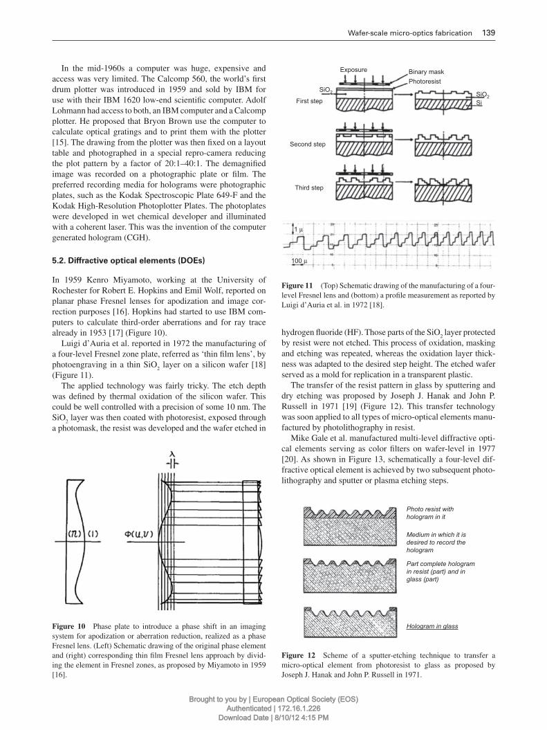
Wafer-scale micro-optics fabrication 139
hydrogen fl uoride (HF). Those parts of the SiO 2 layer protected by resist were not etched. This process of oxidation, masking and etching was repeated, whereas the oxidation layer thick-ness was adapted to the desired step height. The etched wafer served as a mold for replication in a transparent plastic.
The transfer of the resist pattern in glass by sputtering and dry etching was proposed by Joseph J. Hanak and John P. Russell in 1971 [19] (Figure 12 ). This transfer technology was soon applied to all types of micro-optical elements manu-factured by photolithography in resist.
Mike Gale et al. manufactured multi-level diffractive opti-cal elements serving as color fi lters on wafer-level in 1977 [20] . As shown in Figure 13 , schematically a four-level dif-fractive optical element is achieved by two subsequent photo-lithography and sputter or plasma etching steps.
In the mid-1960s a computer was huge, expensive and access was very limited. The Calcomp 560, the world ’ s fi rst drum plotter was introduced in 1959 and sold by IBM for use with their IBM 1620 low-end scientifi c computer. Adolf Lohmann had access to both, an IBM computer and a Calcomp plotter. He proposed that Bryon Brown use the computer to calculate optical gratings and to print them with the plotter [15] . The drawing from the plotter was then fi xed on a layout table and photographed in a special repro-camera reducing the plot pattern by a factor of 20:1 – 40:1. The demagnifi ed image was recorded on a photographic plate or fi lm. The preferred recording media for holograms were photographic plates, such as the Kodak Spectroscopic Plate 649-F and the Kodak High-Resolution Photoplotter Plates. The photoplates were developed in wet chemical developer and illuminated with a coherent laser. This was the invention of the computer generated hologram (CGH).
5.2. Diffractive optical elements (DOEs)
In 1959 Kenro Miyamoto, working at the University of Rochester for Robert E. Hopkins and Emil Wolf, reported on planar phase Fresnel lenses for apodization and image cor-rection purposes [16] . Hopkins had started to use IBM com-puters to calculate third-order aberrations and for ray trace already in 1953 [17] (Figure 10 ).
Luigi d ’ Auria et al. reported in 1972 the manufacturing of a four-level Fresnel zone plate, referred as ‘ thin fi lm lens ’ , by photoengraving in a thin SiO 2 layer on a silicon wafer [18] (Figure 11 ).
The applied technology was fairly tricky. The etch depth was defi ned by thermal oxidation of the silicon wafer. This could be well controlled with a precision of some 10 nm. The SiO 2 layer was then coated with photoresist, exposed through a photomask, the resist was developed and the wafer etched in
Exposure
First step
Second step
Third step
1 μ
100 μ
Binary maskPhotoresist
SiO2SiO2
Si
Figure 11 (Top) Schematic drawing of the manufacturing of a four-level Fresnel lens and (bottom) a profi le measurement as reported by Luigi d ’ Auria et al. in 1972 [18] .
Photo resist withhologram in it
Medium in which it isdesired to record thehologram
Part complete hologramin resist (part) and inglass (part)
Hologram in glass
Figure 12 Scheme of a sputter-etching technique to transfer a micro-optical element from photoresist to glass as proposed by Joseph J. Hanak and John P. Russell in 1971.
Figure 10 Phase plate to introduce a phase shift in an imaging system for apodization or aberration reduction, realized as a phase Fresnel lens. (Left) Schematic drawing of the original phase element and (right) corresponding thin fi lm Fresnel lens approach by divid-ing the element in Fresnel zones, as proposed by Miyamoto in 1959 [16] .
Brought to you by | European Optical Society (EOS)Authenticated | 172.16.1.226
Download Date | 8/10/12 4:15 PM
140 R. Voelkel
5.3. Refractive optical elements (ROEs)
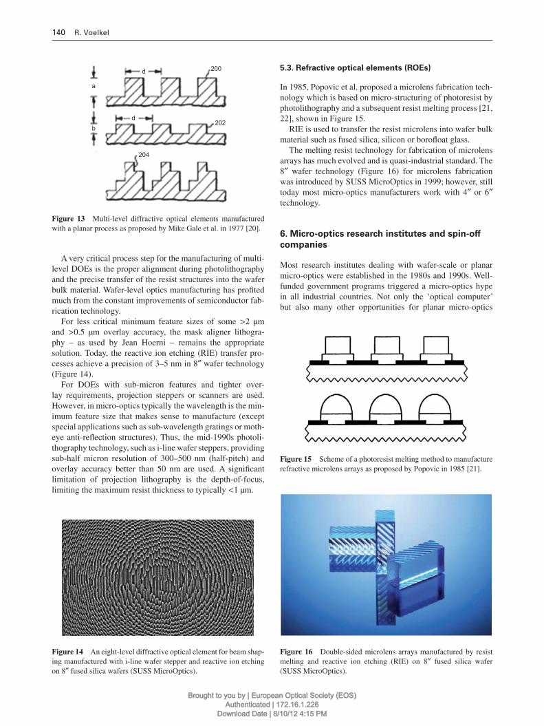
In 1985, Popovic et al. proposed a microlens fabrication tech-nology which is based on micro-structuring of photoresist by photolithography and a subsequent resist melting process [21, 22] , shown in Figure 15 .
RIE is used to transfer the resist microlens into wafer bulk material such as fused silica, silicon or borofl oat glass.
The melting resist technology for fabrication of microlens arrays has much evolved and is quasi-industrial standard. The 8 ″ wafer technology (Figure 16 ) for microlens fabrication was introduced by SUSS MicroOptics in 1999; however, still today most micro-optics manufacturers work with 4 ″ or 6 ″ technology.
6. Micro-optics research institutes and spin-off
companies
Most research institutes dealing with wafer-scale or planar micro-optics were established in the 1980s and 1990s. Well-funded government programs triggered a micro-optics hype in all industrial countries. Not only the ‘ optical computer ’ but also many other opportunities for planar micro-optics
A very critical process step for the manufacturing of multi-level DOEs is the proper alignment during photolithography and the precise transfer of the resist structures into the wafer bulk material. Wafer-level optics manufacturing has profi ted much from the constant improvements of semiconductor fab-rication technology.
For less critical minimum feature sizes of some > 2 µ m and > 0.5 µ m overlay accuracy, the mask aligner lithogra-phy – as used by Jean Hoerni – remains the appropriate solution. Today, the reactive ion etching (RIE) transfer pro-cesses achieve a precision of 3 – 5 nm in 8 ″ wafer technology (Figure 14 ).
For DOEs with sub-micron features and tighter over-lay requirements, projection steppers or scanners are used. However, in micro-optics typically the wavelength is the min-imum feature size that makes sense to manufacture (except special applications such as sub-wavelength gratings or moth-eye anti-refl ection structures). Thus, the mid-1990s photoli-thography technology, such as i-line wafer steppers, providing sub-half micron resolution of 300 – 500 nm (half-pitch) and overlay accuracy better than 50 nm are used. A signifi cant limitation of projection lithography is the depth-of-focus, limiting the maximum resist thickness to typically < 1 µ m.
200
202
204
d
d
a
b
Figure 13 Multi-level diffractive optical elements manufactured with a planar process as proposed by Mike Gale et al. in 1977 [20] .
Figure 14 An eight-level diffractive optical element for beam shap-ing manufactured with i-line wafer stepper and reactive ion etching on 8 ″ fused silica wafers (SUSS MicroOptics).
Figure 15 Scheme of a photoresist melting method to manufacture refractive microlens arrays as proposed by Popovic in 1985 [21] .
Figure 16 Double-sided microlens arrays manufactured by resist melting and reactive ion etching (RIE) on 8 ″ fused silica wafer (SUSS MicroOptics).
Brought to you by | European Optical Society (EOS)Authenticated | 172.16.1.226
Download Date | 8/10/12 4:15 PM
Wafer-scale micro-optics fabrication 141
basic diffractive and refractive micro-optical components. More specialized simulation tools such as VirtualLab [25] , FRED [26] and LayoutLAB [27] use a combination of ray or fi eld tracing, beam or wave propagation or other approxima-tion to simulate the propagation of the light behind micro-optical elements [28] . These tools allow a skilled user to predict and to optimize the performance of a micro-optical element – as long as the illumination is either coherent or fully incoherent.
6.2. Metrology
Micro-optics requires special metrology tools for charac-terization and testing. Neither the test equipment from the semiconductor industry nor the test equipment from classi-cal optics manufacturing completely addresses the metrol-ogy requirements of wafer-level micro-optics. For example, to measure the profi le of an aspherical microlens with 250 µ m lens diameter a special microscope interferometer, which resolves a suffi cient number of fringes over the lens aperture, is required. Often a full array testing of millions of single microlenses on a wafer is needed.
Johannes Schwider et al. started to develop dedicated metrology tools in the 1990s [29 – 32] . Tywman-Green and Mach-Zehnder interferometers have been adapted to measure surface and phase profi les of microlenses with a precision of better than λ /20. Mechanical stylus and contact-less white light profi lometers, confocal microscopes, digital holographic microscopes and surface electron microscopes (SEM) are used in micro-optics fabrication. These instruments are typi-cally modifi ed versions of standard tools and only built in very small series. Typically, the customer and user of micro-optics are not equipped with metrology to test the quality of the micro-optical components by themselves. Customers rely on the information the supplier provides.
System integration of micro-optics follows different rules than the classical optical components such as lenses, prisms, beam splitters, etc. The overall performance of a device using micro-optical components is often not exactly predictable during the design phase. Thus, micro-optics remains some-what ‘ exotic ’ for many optical designers and engineers.
However, micro-optics has much to offer for optical engi-neers. Micro-optics allows to precisely shape illumination light for imaging and projection systems. Micro-optical fi ber couplers, gratings for wavelength multiplexing and switches are essential key components for high-speed communication systems. Micro-optics allows to mass produce high-quality miniaturized optical systems at very attractive costs. The list of innovations using micro-optics is long. This is not such a new phenomenon. Already a hundred years ago research-ers invented devices and systems based on micro-optics. At that time most of these inventions failed, because no suitable fabrication technology for micro-optics was available. In the following section, we will explain how semiconductor wafer technology now allows fabricating micro-optics with high precision on a wafer-scale. We will report on recent trends in wafer-scale optics manufacturing, testing and packaging and present typical applications.
in medicine, biology, optical communication networks and other applications were on the horizon. The optics community hoped to repeat the semiconductor hype in generating infi nite growth and wealth of a planar optics industry similar to the integrated circuit explosion in Silicon Valley.
The fi rst companies for fabrication micro-optics were spun-off approximately 10 years later from these research institutes. However, neither the optical computer, nor the later called Photonics hype really took off. Micro-optics could not redo what the semiconductor industry had done. The fundamental difference is that electronics allows the building of complete devices including input sensor, CPU, memory and output, a display, sound or movement. Optics and micro-optical elements are typically only parts of a larger mechanic or electronic device used to redirect, shape or switch the light. Fortunately, they are often key enabling parts that signifi cantly improve the performance of the com-plete device.
Micro-optics is an established mature product, but it remains a niche product, not a big growth area or big busi-ness. Even today the supplier ’ s base for micro-optics is rela-tively small where large multi-billion companies purchase their micro-optics from small- and medium-size suppliers.
A more fundamental limitation of micro-optics is related to the nature of light. Electronics still follows Gordon Moore ’ s Law from 1965 and is constantly reducing the component size thus increasing functionality. In optics, there is no scaling for the wavelength and scaling of the micro-optics to improve the performance does not make sense.
6.1. Raytracing and simulation
A major problem for the acceptance of planar micro-optics was – and partially still is – the availability of software tools for proper simulation, optimization and system integration. Standard optical design software often does not allow simu-lating and modeling of diffractive and refractive micro-optical elements (Figure 17 [23] ).
Diffraction, scattering and interference effects from micro-optical elements could be fairly complex: Moir é effects in stacked microlens arrays, intensity modulation in laser beam shapers, ghost images of diffractive optical elements, scat-tering, speckles – are only some of the possible issues in simulating micro-optics [24] . The situation is improving, more and more optical design programs have integrated
Figure 17 Photographs of (left) refractive microlens arrays (ROEs) and (right) random diffuser plate for beam smoothing [23] , both manufactured on 8 ″ (200 mm) wafers of fused silica (SUSS MicroOptics).
Brought to you by | European Optical Society (EOS)Authenticated | 172.16.1.226
Download Date | 8/10/12 4:15 PM
142 R. Voelkel
parallel to the newer 300 mm fabs. For example, old 200 mm DRAM fabs are now used for mass production of complementary CMOS image sensors and MEMS devices. This is a strong argument to opt for 200 mm micro-optics technology. Equipment manufacturers remain interested in updating their 200 mm tools. Novel technology trends, such as wafer-level packaging (WLP), thin-wafer handling and TSV/3D-IC, are also available for 200 mm wafer-manufac-turing equipment.
7.2. Wafer cleaning and photoresist coating
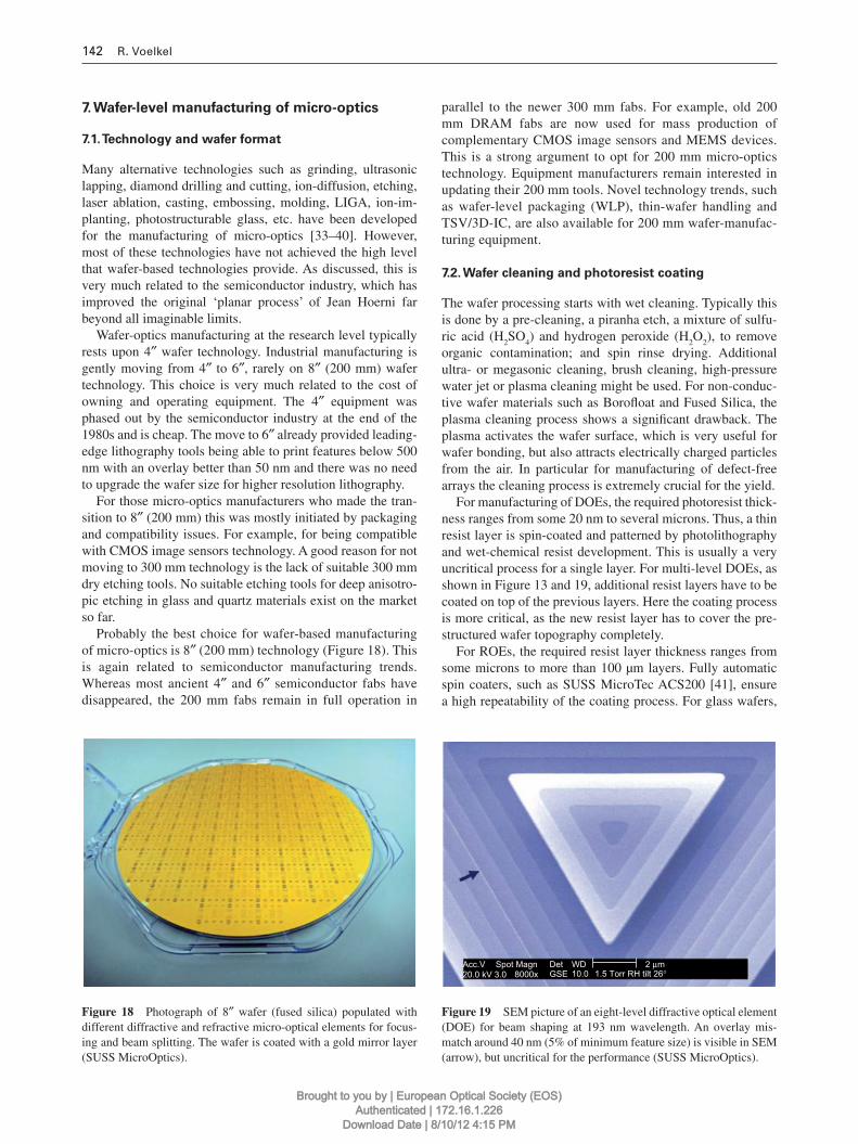
The wafer processing starts with wet cleaning. Typically this is done by a pre-cleaning, a piranha etch, a mixture of sulfu-ric acid (H 2 SO 4 ) and hydrogen peroxide (H 2 O 2 ), to remove organic contamination; and spin rinse drying. Additional ultra- or megasonic cleaning, brush cleaning, high-pressure water jet or plasma cleaning might be used. For non-conduc-tive wafer materials such as Borofl oat and Fused Silica, the plasma cleaning process shows a signifi cant drawback. The plasma activates the wafer surface, which is very useful for wafer bonding, but also attracts electrically charged particles from the air. In particular for manufacturing of defect-free arrays the cleaning process is extremely crucial for the yield.
For manufacturing of DOEs, the required photoresist thick-ness ranges from some 20 nm to several microns. Thus, a thin resist layer is spin-coated and patterned by photolithography and wet-chemical resist development. This is usually a very uncritical process for a single layer. For multi-level DOEs, as shown in Figure 13 and 19 , additional resist layers have to be coated on top of the previous layers. Here the coating process is more critical, as the new resist layer has to cover the pre-structured wafer topography completely.
For ROEs, the required resist layer thickness ranges from some microns to more than 100 µ m layers. Fully automatic spin coaters, such as SUSS MicroTec ACS200 [41] , ensure a high repeatability of the coating process. For glass wafers,
7. Wafer-level manufacturing of micro-optics
7.1. Technology and wafer format
Many alternative technologies such as grinding, ultrasonic lapping, diamond drilling and cutting, ion-diffusion, etching, laser ablation, casting, embossing, molding, LIGA, ion-im-planting, photostructurable glass, etc. have been developed for the manufacturing of micro-optics [33 – 40] . However, most of these technologies have not achieved the high level that wafer-based technologies provide. As discussed, this is very much related to the semiconductor industry, which has improved the original ‘ planar process ’ of Jean Hoerni far beyond all imaginable limits.
Wafer-optics manufacturing at the research level typically rests upon 4 ″ wafer technology. Industrial manufacturing is gently moving from 4 ″ to 6 ″ , rarely on 8 ″ (200 mm) wafer technology. This choice is very much related to the cost of owning and operating equipment. The 4 ″ equipment was phased out by the semiconductor industry at the end of the 1980s and is cheap. The move to 6 ″ already provided leading-edge lithography tools being able to print features below 500 nm with an overlay better than 50 nm and there was no need to upgrade the wafer size for higher resolution lithography.
For those micro-optics manufacturers who made the tran-sition to 8 ″ (200 mm) this was mostly initiated by packaging and compatibility issues. For example, for being compatible with CMOS image sensors technology. A good reason for not moving to 300 mm technology is the lack of suitable 300 mm dry etching tools. No suitable etching tools for deep anisotro-pic etching in glass and quartz materials exist on the market so far.
Probably the best choice for wafer-based manufacturing of micro-optics is 8 ″ (200 mm) technology (Figure 18 ). This is again related to semiconductor manufacturing trends. Whereas most ancient 4 ″ and 6 ″ semiconductor fabs have disappeared, the 200 mm fabs remain in full operation in
Acc.V20.0 kV 3.0 8000x
Spot Magn DetGSE
WD10.0 1.5 Torr RH tilt 26°
2 μm
Figure 19 SEM picture of an eight-level diffractive optical element (DOE) for beam shaping at 193 nm wavelength. An overlay mis-match around 40 nm (5 % of minimum feature size) is visible in SEM (arrow), but uncritical for the performance (SUSS MicroOptics).
Figure 18 Photograph of 8 ″ wafer (fused silica) populated with different diffractive and refractive micro-optical elements for focus-ing and beam splitting. The wafer is coated with a gold mirror layer (SUSS MicroOptics).
Brought to you by | European Optical Society (EOS)Authenticated | 172.16.1.226
Download Date | 8/10/12 4:15 PM
Wafer-scale micro-optics fabrication 143
DOEs have a major impact on the reduction of aberrations and diffraction effects in projection lithography allowing a resolution enhancement from 250 nm to 45 nm within the past decade.
Recently, ASML has introduced an array of micro-mir-rors for pupil shaping, FlexRay ™ programmable illumina-tion technology, which is the new standard for leading-edge ASML immersion steppers shown in Figure 21 (bottom, right). Microlens arrays are used for mirror array illumination and for mirror-position control.
7.4. Photolithography and resist melting for refractive
microlenses
Owing to a very limited depth-of-focus, projection lithogra-phy tools are not well suited for thick resist exposure. Thus, mask aligners in contact or proximity mode are the preferred lithography tool. Contact lithography allows fi ne details to be resolved, but requires particle-free surfaces and frequent mask cleaning. In production, mask aligners are usually used in proximity mode, whereas the mask is at a distance of some 10 – 30 µ m above the wafer. Thick fi lm photoresists, such as AZ 4562, AZ 9260 or AZ 40XT, are optimized for mask aligner lithography [45] . Some thick resists even show a light guiding characteristic during the exposure process. Exposed areas become transparent and guide the exposure light lin-early in deeper resist regions. Typically, an aspect ratio of 5 – 7 is achieved with good sidewalls for thick resist layers. Consequently, for a 50 µ m thick resist layer a lens-to-lens gap of some 7 µ m is required to avoid deformation of the lens profi le during the resist melting process.
After wet-chemical development and drying, the resist structures are melted in an oven or on a hotplate at tempera-tures around 150 ° C – 180 ° C. The melting procedure itself is
edge-handling tooling is used to improve uniformity. For melting resist technology shown in Figure 15, uniformity of the resist layer is directly related to the uniformity of the microlenses after melting. Thus, a wafer mapping of the resist allows monitoring quality at an early stage of the manufactur-ing process.
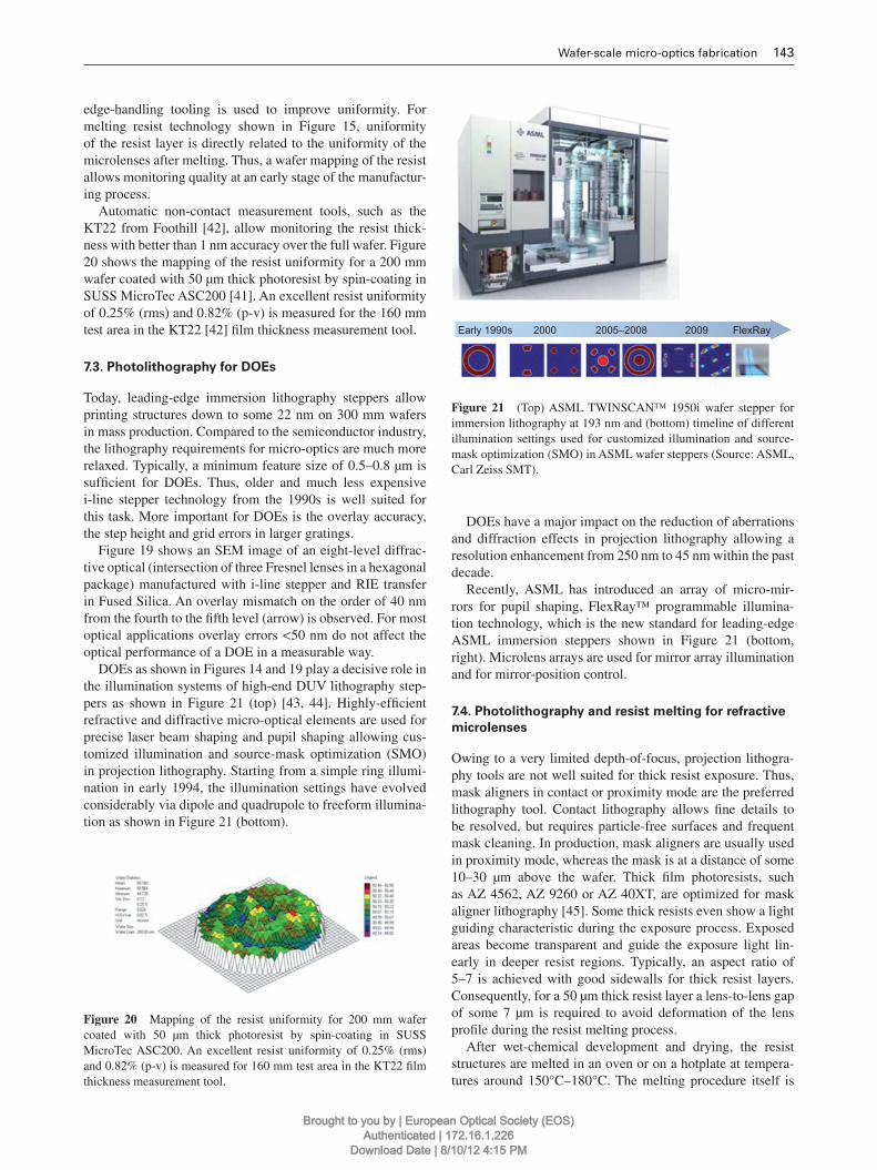
Automatic non-contact measurement tools, such as the KT22 from Foothill [42] , allow monitoring the resist thick-ness with better than 1 nm accuracy over the full wafer. Figure 20 shows the mapping of the resist uniformity for a 200 mm wafer coated with 50 µ m thick photoresist by spin-coating in SUSS MicroTec ASC200 [41] . An excellent resist uniformity of 0.25 % (rms) and 0.82 % (p-v) is measured for the 160 mm test area in the KT22 [42] fi lm thickness measurement tool.
7.3. Photolithography for DOEs
Today, leading-edge immersion lithography steppers allow printing structures down to some 22 nm on 300 mm wafers in mass production. Compared to the semiconductor industry, the lithography requirements for micro-optics are much more relaxed. Typically, a minimum feature size of 0.5 – 0.8 µ m is suffi cient for DOEs. Thus, older and much less expensive i-line stepper technology from the 1990s is well suited for this task. More important for DOEs is the overlay accuracy, the step height and grid errors in larger gratings.
Figure 19 shows an SEM image of an eight-level diffrac-tive optical (intersection of three Fresnel lenses in a hexagonal package) manufactured with i-line stepper and RIE transfer in Fused Silica. An overlay mismatch on the order of 40 nm from the fourth to the fi fth level (arrow) is observed. For most optical applications overlay errors < 50 nm do not affect the optical performance of a DOE in a measurable way.
DOEs as shown in Figures 14 and 19 play a decisive role in the illumination systems of high-end DUV lithography step-pers as shown in Figure 21 (top) [43, 44] . Highly-effi cient refractive and diffractive micro-optical elements are used for precise laser beam shaping and pupil shaping allowing cus-tomized illumination and source-mask optimization (SMO) in projection lithography. Starting from a simple ring illumi-nation in early 1994, the illumination settings have evolved considerably via dipole and quadrupole to freeform illumina-tion as shown in Figure 21 (bottom).
Figure 20 Mapping of the resist uniformity for 200 mm wafer coated with 50 µ m thick photoresist by spin-coating in SUSS MicroTec ASC200. An excellent resist uniformity of 0.25 % (rms) and 0.82 % (p-v) is measured for 160 mm test area in the KT22 fi lm thickness measurement tool.
Early 1990s 2000 2005–2008 2009 FlexRay
Figure 21 (Top) ASML TWINSCAN ™ 1950i wafer stepper for immersion lithography at 193 nm and (bottom) timeline of different illumination settings used for customized illumination and source-mask optimization (SMO) in ASML wafer steppers (Source: ASML, Carl Zeiss SMT).
Brought to you by | European Optical Society (EOS)Authenticated | 172.16.1.226
Download Date | 8/10/12 4:15 PM
144 R. Voelkel
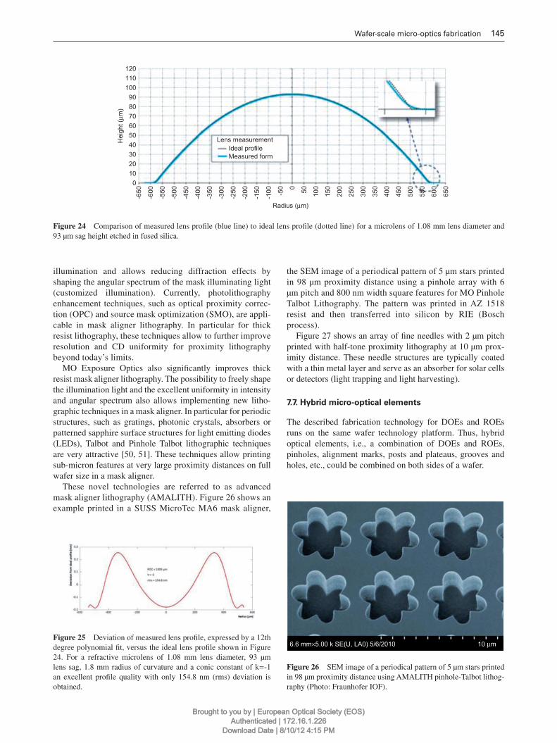
320 nm subdivided to 16 phase levels. A diffraction effi ciency of 98 % and < 0.1 % in the 0th diffraction order was achieved for a 16-level DOE shown in Figure 23.
Melted resist lenses are usually very close to a spheri-cal lens profi le with a conic around k ≈ 0 after melting. The transfer of the melted resist lens by RIE allows changing the lens profi le. This is done by varying the mixture of the etch gases and oxygen during the etch process. If the etch rate for resist is higher than for the wafer bulk material, the resulting lens profi le will be fl atter than the resist lens pro-fi le. A continuous change of all etch parameters allows to obtain aspherical lens profi les. For both DOEs and ROEs, the RIE process should be anisotropic (vertical) to allow a perfect shape control. The remaining horizontal component leads, e.g., to a shrinkage of the lens diameter for refractive microlenses.
Figure 24 shows the comparison of the measured lens pro-fi le (blue line) to the desired lens profi le (dotted line) of a microlens with 1.08 mm lens diameter and 93 µ m lens sag height etched in silica. The profi le was measured in a KLA-Tencor P15 mechanical profi lometer [48] . Figure 25 shows the deviation of the measured lens profi le, expressed by a 12th degree polynomial fi t, to the ideal lens profi le. For a microl-ens of 1.08 mm lens diameter, 93 µ m lens sag, 1.8 mm radius of curvature and a conic constant of k = -1 a deviation of only 154.8 nm (rms) is obtained.
Melting resist technology and subsequent RIE allows manufacturing aspherical microlenses with excellent profi le accuracy and lens-to-lens uniformity on full wafer level. The described technology is based on planar wafer technology from semiconductor manufacturing and has been developed to a very high level. Excellent uniformity for lens-to-lens and wafer-to-wafer allows providing high quality microlenses in hard durable material for very competitive pricing.
7.6. Advanced mask aligner lithography (AMALITH)
for micro-optics manufacturing
Recently, mask aligner lithography was signifi cantly improved by a novel illumination system referred to as MO Exposure Optics [49] . MO Exposure Optics improves the uniformity of the illumination light, provides telecentric
fairly simple [46] . Above the softening temperature the edges of the resist structure start melting. Above the glass transition temperature the amorphous resist polymer changes into a glass state system. The surface tension tries to minimize the surface area by rearranging the liquid masses inside the drop. Ideally, the resist melts completely, the masses are freely transported and surface tension forms a spherical microlens. In practice, the lens melting process needs careful process optimization and precise control of all process parameters to obtain good lens-to-lens uniformity within one wafer and from wafer-to-wafer. Repeatability and uniformity of melted resist lenses are key factors for the following etch process.
7.5. Reactive ion etching (RIE)
In the next step the micro-optical structures are transferred into the bulk wafer material, typically by plasma ion etch-ing. For wafer processing, RIE, where chemical reaction of the etch gases such as SF 6 and CHF 3 is enhanced by the ion bombardment, is the preferred choice. The etching process removes atoms from the resist and wafer surface at different etch rates. Surface areas covered by resist structures are pro-tected until the covering resist layer is removed.
Typical etch rates range from < 0.01 µ m/min to approxi-mately 1 µ m/min depending on the ion energy and reactive etch gases in the plasma chamber. Slow etch rates are pre-ferred for diffractive optical elements with only small etch depths. For the transfer of refractive resist lenses a faster etch-ing process is preferred to reduce the total etching time.
The optical performance of a DOE is determined by dif-fraction effi ciency and noise level, i.e., the percentage of light in the 0th order, spurious orders and ghost images. To obtain a high optical performance, a correct etch depth on the order of λ /20 is required.
Figure 22 shows the phase profi le of 16-level DOEs for focus spot generation, measured in a white light profi lometer Wyko NT3300 [47] . Figure 23 shows a scan of the x-profi le from the same measurement showing a total phase depth of
Figure 22 Phase profi le of a densely packed array of 16-level dif-fractive optical elements for focus spot generation, measured in a white light profi lometer Wyko NT3300 (SUSS MicroOptics).
50nm
-50
-100
-150
-200
-250
0 50 100 150
X: 238.6 μm
200 250 300μm
0
Figure 23 Scan of the profi le in x-direction of the diffractive opti-cal element shown above. The total phase depth of 320 nm subdi-vided into 16 phase levels.
Brought to you by | European Optical Society (EOS)Authenticated | 172.16.1.226
Download Date | 8/10/12 4:15 PM
Wafer-scale micro-optics fabrication 145
illumination and allows reducing diffraction effects by shaping the angular spectrum of the mask illuminating light (customized illumination). Currently, photolithography enhancement techniques, such as optical proximity correc-tion (OPC) and source mask optimization (SMO), are appli-cable in mask aligner lithography. In particular for thick resist lithography, these techniques allow to further improve resolution and CD uniformity for proximity lithography beyond today ’ s limits.
MO Exposure Optics also signifi cantly improves thick resist mask aligner lithography. The possibility to freely shape the illumination light and the excellent uniformity in intensity and angular spectrum also allows implementing new litho-graphic techniques in a mask aligner. In particular for periodic structures, such as gratings, photonic crystals, absorbers or patterned sapphire surface structures for light emitting diodes (LEDs), Talbot and Pinhole Talbot lithographic techniques are very attractive [50, 51] . These techniques allow printing sub-micron features at very large proximity distances on full wafer size in a mask aligner.
These novel technologies are referred to as advanced mask aligner lithography (AMALITH). Figure 26 shows an example printed in a SUSS MicroTec MA6 mask aligner,
120110100
90
Hei
ght (
μm) 80
70605040302010
0
-650
-600
-550
-500
-450
-400
-350
-300
-250
Lens measurementIdeal profileMeasured form
-200
-150
-100 -5
0 0 50 100
150
200
250
300
350
400
450
500
550
600
Radius (μm)
650
Figure 24 Comparison of measured lens profi le (blue line) to ideal lens profi le (dotted line) for a microlens of 1.08 mm lens diameter and 93 µ m sag height etched in fused silica.
Figure 25 Deviation of measured lens profi le, expressed by a 12th degree polynomial fi t, versus the ideal lens profi le shown in Figure 24. For a refractive microlens of 1.08 mm lens diameter, 93 µ m lens sag, 1.8 mm radius of curvature and a conic constant of k = -1 an excellent profi le quality with only 154.8 nm (rms) deviation is obtained.
6.6 mm×5.00 k SE(U, LA0) 5/6/2010 10 μm
Figure 26 SEM image of a periodical pattern of 5 µ m stars printed in 98 µ m proximity distance using AMALITH pinhole-Talbot lithog-raphy (Photo: Fraunhofer IOF).
the SEM image of a periodical pattern of 5 µ m stars printed in 98 µ m proximity distance using a pinhole array with 6 µ m pitch and 800 nm width square features for MO Pinhole Talbot Lithography. The pattern was printed in AZ 1518 resist and then transferred into silicon by RIE (Bosch process).
Figure 27 shows an array of fi ne needles with 2 µ m pitch printed with half-tone proximity lithography at 10 µ m prox-imity distance. These needle structures are typically coated with a thin metal layer and serve as an absorber for solar cells or detectors (light trapping and light harvesting).
7.7. Hybrid micro-optical elements
The described fabrication technology for DOEs and ROEs runs on the same wafer technology platform. Thus, hybrid optical elements, i.e., a combination of DOEs and ROEs, pinholes, alignment marks, posts and plateaus, grooves and holes, etc., could be combined on both sides of a wafer.
Brought to you by | European Optical Society (EOS)Authenticated | 172.16.1.226
Download Date | 8/10/12 4:15 PM
146 R. Voelkel
Although described fabrication technology is based on semi-conductor equipment and standards, most of their metrology tools are not suitable for micro-optics testing. Micro-optical elements are usually too big and too high for test tools derived for the inspection of sub-micron structures; inspection tools cannot derive a 3D lens profi le of a microlens. In addition, state-of-the-art tools from semiconductor industry are usually very expensive, because they are designed for 300 mm wafers and very high throughput. Unfortunately, measurement tools from the optics industry do not fi t well for micro-optics either. Interferometers designed for large classical lenses can-not resolve the profi le of a tiny microlens. Mechanical stylus profi lometers work well to measure the etch depth of diffrac-tive elements, line scans of microlens profi les and to control the lens sag at different points of a wafer. However, they do not provide 3D profi le information about a structure and they
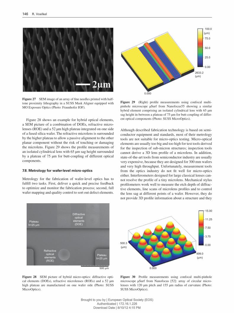
Figure 28 shows an example for hybrid optical elements, a SEM picture of a combination of DOEs, refractive micro-lenses (ROE) and a 52 µ m high plateau integrated on one side of a fused silica wafer. The refractive microlens is surrounded by the higher plateau to allow a passive alignment to the other planar component without the risk of touching or damaging the microlens. Figure 29 shows the profi le measurements of an isolated cylindrical lens with 65 µ m sag height surrounded by a plateau of 75 µ m for butt-coupling of different optical components.
7.8. Metrology for wafer-level micro-optics
Metrology for the fabrication of wafer-level optics has to fulfi ll two tasks. First, deliver a quick and precise feedback to optimize and monitor the fabrication process; second, full wafer mapping and quality control to sort out defect elements.
Figure 27 SEM image of an array of fi ne needles printed with half-tone proximity lithography in a SUSS Mask Aligner equipped with MO Exposure Optics (Photo: Fraunhofer IOF).
Diffractiveoptical
elements(DOE)
Refractiveoptical
elements(ROE)
Plateauh=25 μm
Plateauh=25 μm
500 μm
Figure 28 SEM picture of hybrid micro-optics: diffractive opti-cal elements (DOEs), refractive microlenses (ROEs) and a 52 µ m high plateau are manufactured on one wafer side (Photo: SUSS MicroOptics).
15.00
11.25
7.50
3.75
0.00
499.0
0.000
(μm)
500.3(μm)
Figure 30 Profi le measurements using confocal multi-pinhole microscope µ Surf from Nanofocus [52] : array of circular micro-lenses with 120 µ m pitch and 155 µ m radius of curvature (Photo: SUSS MicroOptics).
100.0
75.0
50.0
25.0
0.00
2633.2
0.000
(μm)
(μm)
Figure 29 (Right) profi le measurements using confocal multi-pinhole microscope µ Surf from Nanofocus55 showing a similar hybrid element comprising an isolated cylindrical lens with 65 µ m sag height in-between a plateau of 75 µ m for butt-coupling of differ-ent optical components (Photo: SUSS MicroOptics).
Brought to you by | European Optical Society (EOS)Authenticated | 172.16.1.226
Download Date | 8/10/12 4:15 PM
Wafer-scale micro-optics fabrication 147
7.9. Wafer-level packaging of micro-optics
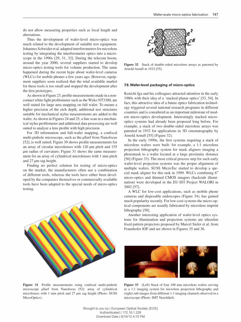
Kenichi Iga and his colleagues attracted attention in the early 1980s with their idea of a ‘ stacked planar optics ’ [53, 54] . In fact, this attractive idea of a future optics fabrication technol-ogy triggered several national research programs in different countries and is considered as an important milestone of mod-ern micro-optics development. Interestingly stacked micro-optics systems had already been proposed long before. For example, a stack of two double-sided microlens arrays was patented in 1932 for applications in 3D cinematography by Arnold Arnulf [55] (Figure 32 ).
In the early 1990s, the fi rst systems requiring a stack of microlens wafers were built: for example, a 1:1 microlens projection lithography system for mask aligners imaging a photomask to a wafer located at a large proximity distance [56] (Figure 33 ). The most critical process step for such early wafer-level projection systems was the proper alignment of multiple wafers. SUSS MicroTec started to develop a spe-cial mask aligner for this task in 1999. WLCs combining 6 ″ micro-optics and thinned CMOS imagers (backside illumi-nation) were developed in the EU-IST Project WALORI in 2002 [57] .
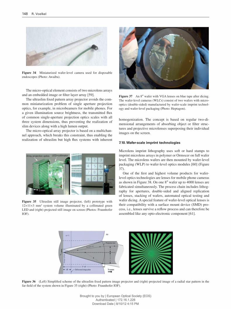
A WLC for low-cost applications, such as mobile phone cameras and disposable endoscopes (Figure 34 ), has gained much popularity recently. For low-cost systems the micro-op-tical components are usually fabricated by microlens imprint lithography [58] .
Another interesting application of wafer-level optics sys-tems for illumination and projection systems are ultraslim fi xed pattern projectors proposed by Marcel Sieler et al. from Fraunhofer IOF and are shown in Figures 35 and 36 .
do not allow measuring properties such as focal length and aberrations.
Thus the development of wafer-level micro-optics was much related to the development of suitable test equipment. Johannes Schwider et al. adapted interferometers for microlens testing by integrating the interferometer optics into a micro-scope in the 1990s [29, 31, 32] . During the telecom boom, around the year 2000, several suppliers started to develop micro-optics testing tools for volume production. The same happened during the recent hype about wafer-level cameras (WLCs) for mobile phones a few years ago. However, equip-ment suppliers soon realized that the total available market for these tools is too small and stopped the development after the fi rst prototypes.
As shown in Figure 23, profi le measurements made in a non-contact white light profi lometer such as the Wyko NT3300, are well suited for large area mapping on full wafer. To ensure a higher precision of the etch depth, additional test structures suitable for mechanical stylus measurements are added to the wafer. As shown in Figures 24 and 25, a line scan in a mechan-ical stylus profi lometer and additional data processing are well suited to analyze a lens profi le with high precision.
For 3D information and full-wafer mapping, a confocal multi-pinhole microscope, such as the µ Surf from Nanofocus [52] , is well suited. Figure 30 shows profi le measurements for an array of circular microlenses with 120 µ m pitch and 155 µ m radius of curvature; Figure 31 shows the same measure-ment for an array of cylindrical microlenses with 1 mm pitch and 27 µ m sag height.
Finding no perfect solution for testing of micro-optics on the market, the manufacturers often use a combination of different tools, whereas the tools have either been devel-oped by the companies themselves or commercially available tools have been adapted to the special needs of micro-optics testing.
Figure 31 Profi le measurements using confocal multi-pinhole microscope µ Surf from Nanofocus [52] : array of cylindrical microlenses with 1 mm pitch and 27 µ m sag height (Photo: SUSS MicroOptics).
Figure 32 Stack of double-sided microlens arrays as patented by Arnold Arnulf in 1932 [55] .
Figure 33 (Left) Stack of four 100 mm microlens wafers serving as a 1:1 imaging system for microlens projection lithography and (right) sub-images from different 1:1 imaging channels observed in a microscope (Photo: IMT Neuch â tel).
Brought to you by | European Optical Society (EOS)Authenticated | 172.16.1.226
Download Date | 8/10/12 4:15 PM
148 R. Voelkel
The micro-optical element consists of two microlens arrays and an embedded image or fi lter layer array [59] .
The ultraslim fi xed pattern array projector avoids the com-mon miniaturization problem of single aperture projection optics, for example, in microbeamers for mobile phones. For a given illumination source brightness, the transmitted fl ux of common single-aperture projection optics scales with all three system dimensions, thus preventing the realization of slim devices along with a high lumen output.
The micro-optical array projector is based on a multichan-nel approach, which breaks this constraint, thus enabling the realization of ultraslim but high fl ux systems with inherent
Figure 34 Miniaturized wafer-level camera used for disposable endoscopes (Photo: Awaiba).
Array projection optics
3 mm
LED+collimator
Figure 35 Ultraslim still image projector, (left) prototype with 12 × 11 × 3 mm 3 system volume illuminated by a collimated green LED and (right) projected still image on screen (Photos: Fraunhofer IOF).
Figure 36 (Left) Simplifi ed scheme of the ultraslim fi xed pattern image projector and (right) projected image of a radial star pattern in the far-fi eld of the system shown in Figure 35 (right) (Photo: Fraunhofer IOF).
Figure 37 An 8 ″ wafer with VGA lenses on blue tape after dicing. The wafer-level cameras (WLCs) consist of two wafers with micro-optics (double-sided) manufactured by wafer-scale imprint technol-ogy and wafer-level packaging (Photo: Heptagon).
homogenization. The concept is based on regular two-di-mensional arrangements of absorbing object or fi lter struc-tures and projective microlenses superposing their individual images on the screen.
7.10. Wafer-scale imprint technologies
Microlens imprint lithography uses soft or hard stamps to imprint microlens arrays in polymer or Ormocer on full wafer level. The microlens wafers are then mounted by wafer-level packaging (WLP) to wafer-level optics modules [60] (Figure 37 ).
One of the fi rst and highest volume products for wafer-level optics technologies are lenses for mobile phone cameras as shown in Figure 38 . On one 8 ″ wafer up to 4000 lenses are fabricated simultaneously. The process chain includes lithog-raphy for apertures, double-sided and aligned replication of lenses, stacking of wafers, automated optical testing and wafer dicing. A special feature of wafer-level optical lenses is their compatibility with a surface mount device (SMD) pro-cess, i.e., lenses survive a refl ow process and can therefore be assembled like any opto-electronic component [61] .
Brought to you by | European Optical Society (EOS)Authenticated | 172.16.1.226
Download Date | 8/10/12 4:15 PM
Wafer-scale micro-optics fabrication 149
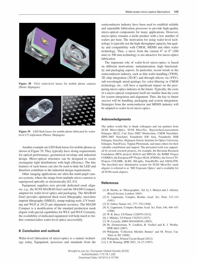
semiconductor industry have been used to establish reliable and repeatable fabrication processes to provide high-quality micro-optical components for many applications. However, micro-optics remains a niche product with a low number of wafers per hour. The motivation for using wafer-level tech-nology is typically not the high-throughput capacity, but qual-ity and compatibility with CMOS, MEMS and other wafer technology. Thus, a move from the current 6 ″ or 8 ″ (200 mm) to 300 mm technology is not attractive for micro-optics fabrication.
The important role of wafer-level micro-optics is based on different motivations: miniaturization, high functional-ity and packaging aspects. In particular, recent trends in the semiconductor industry, such as thin wafer handling (TWH), 3D chip integration (3D-IC) and through-silicon via (TSV), sub-wavelength metal-gratings for color-fi ltering in CMOS technology, etc., will have a signifi cant impact on the pros-pering micro-optics industry in the future. Typically, the costs of a micro-optical component itself are smaller than the costs for system integration and alignment. Thus, the key to future success will be handling, packaging and system integration. Strategies from the semiconductor and MEMS industry will be adapted to wafer-level micro-optics.
Acknowledgments
The author would like to thank colleagues and our partners from SUSS Micro-Optics, SUSS MicroTec, BayerischesLaserzentrum Erlangen (BLZ), Carl Zeiss SMT Oberkochen, CSEM Neuch â tel, EPFL-IMT Neuchatel, Fraunhofer IOF Jena, Fraunhofer IISB Erlangen, GenySys, Heptagon Zurich, Institute for Optics University Erlangen, NanoFocus, Toppan Photomask, and many others for their valuable contribution and support. The presented work was support-ed by several research projects, for example, the Bavarian Research Foundation (BFS) projects MALS and MINAS, the BMBF Project COMIKA, the European FP7 Project SEAL (FISMA), the Swiss CTI-Projects COLMIR, ALBS, HiLights, NanoHyMo and AMALITH. The described new illumination system for SUSS MicroTec mask aligners is referred to as ‘ MO Exposure Optics ’ and is available for all SUSS mask aligners.
References
[1] R. Hooke, in ‘ Micrographia ’ , Ed. by J. Martyn and J. Allestry (Royal Society, London, 1665).
[2] G. Lippmann, Comptes Rendus Acad. Sci. Paris 112 – 114 (1891).
[3] D. Gabor, Nature 161, 777 – 778 (1948). [4] G. Lippmann, Comptes Rendus Acad. Sci. Paris 146, 446 – 451
(1908). [5] W. R. Hess, US Patent 1128979 (1912). [6] J. Mihalyi, US Patent 1762932 (1927). [7] W. Cassarly, ISBN 081944894X (2003). [8] M. Zimmermann, N. Lindlein, R. Voelkel and K. J. Weible,
SPIE 6663 (2007). [9] Wikipedia ‘ Collection Mich è le Bonnet ’ and M. Frizot, Cat.
‘ Paris in 3D ’ (2000). [10] Wikipedia, Printed Circuit Board (2012). [11] J. H. Bruning, SPIE 3051, 14 – 27 (1997).
Another example are LED fl ash lenses for mobile phones as shown in Figure 39 . They typically have strong requirements for optical performance, geometrical envelope and industrial design. Micro-optical structures can be designed to create rectangular light distributions with high effi ciency. The fi ne features of such lenses can also be used to hide the LED and therefore contribute to the industrial design requirements.
Other imaging applications are ultra-fl at multi-pupil cam-era systems, where the image from multiple micro-cameras is superposed optically or electronically [62, 63] .
Equipment suppliers now provide dedicated mask align-ers, e.g., the SUSS MA/BA8 Gen3 and the MA200 Compact, adapted for wafer-level optics and packaging. The MA/BA8 Gen3 provides optimized thick resist lithography, microlens imprint lithography (SMILE), stamp making tools, UV bond-ing and WLP at ± 0.25 µ m alignment accuracy. The MA200 Compact is a modifi cation of the standard production mask aligner with special capabilities for WLC and WLP. Certainly, the availability of dedicated equipment will help much to fur-ther commercialize wafer-level optics successfully.
8. Conclusion and outlook
Wafer-level fabrication of micro-optics is a mature technol-ogy today. Equipment, processes and standards from the
Figure 38 VGA wafer-level lenses for mobile phone cameras (Photo: Heptagon).
Figure 39 LED fl ash lenses for mobile phone fabricated by wafer-level UV replication (Photos: Heptagon).
Brought to you by | European Optical Society (EOS)Authenticated | 172.16.1.226
Download Date | 8/10/12 4:15 PM
150 R. Voelkel
Dr. Reinhard Voelkel received his Diploma in Physics in 1989 and his PhD in 1994 from the University of Erlangen-Nuernberg, Germany, where he worked at the Applied Optics Institute (under Prof. Adolf W. Lohmann and Prof. Johannes Schwider) on holographic
optical elements for optical interconnects and backplanes.
After his PhD he worked at the Institute of Microtechnology (under Prof. Ren é Dandliker and Prof. Hans Peter Herzig) at the University of Neuchatel, Switzerland, on micro-optics for biosensors, for optical interconnects, for photolitho-graphy systems and miniaturized imaging and camera sys-tems. Reinhard Voelkel is the co-founder and CEO of SUSS MicroOptics, a leading supplier of micro-optical components and systems located in Neuch â tel, Switzerland. He is a mem-ber of the German Optical Society (DGaO), the Swiss Optical Society (SSOM), the European Optical Society (EOS), SPIE and the Optical Society of America (OSA).
[12] J. R. Nall and J. W. Lathrop, Int. Electron Devices Meeting (1957).
[13] J. A. Hoerni, US Patent 3025589 (1959). [14] R. Noyce, US Patent 2,981,877 (1959). [15] B. R. Brown and A. W. Lohmann, Appl. Opt. 5, 967 – 969
(1966). [16] K. Miyamoto, J. Opt. Soc. Am. 51, 17 – 20 (1961). [17] R. E. Hopkins and G. Spence, J. Opt. Soc. Am. 52, 2 (1962). [18] L. d ’ Auria, J. P. Huignard, A. M. Roy and E. Spitz, Opt. Comm.
5, 232 – 235 (1972). [19] J. J. Hanak and J. P. Russell, US Patent 3733258 (1971). [20] M. T. Gale, H. W. Lehmann and R. W. Widmer, US Patent
4155627 (1977). [21] Z. D. Popovic, R. A. Sprague and G. A. Neville Connell, US
Patent 4689291 (1985). [22] D. Daly, R. F. Stevens, M. C. Hutley and N. Davies, J. Meas.
Sci. Technol. 1, 759 – 766 (1990). [23] P. Ruffi eux, T. Scharf, I. Philipoussis, H. P. Herzig, R. Voelkel,
et al. Opt. Exp. 16, 19541 – 19549 (2008). [24] N. Lindlein, F. Simon and J. Schwider, Opt. Eng. 37, 1809
(1998). [25] VirtualLab ™ , LightTrans ( www.lighttrans.com ). [26] FRED ™ , Photon Engineering. [27] LayoutLAB ™ , GenISys ( www.genisys-gmbh.de ). [28] P. Ruffi eux, T. Scharf, H. P. Herzig, R. Voelkel and K. J. Weible,
Opt. Expr. 14, 4687 – 4694 (2006). [29] Th. Dresel, A. Horstmann, A. Otto and J. Schwider, Pure Appl.
Opt. (UK) 1, 241 (1992). [30] R. Voelkel, S. Rosner, H. Kobolla, J. Schmidt, J. Schwider,
et al., J. Mod. Opt. (UK) 40, 1787 (1993). [31] J. Schwider and O. Falkenstorfer, Opt. Eng. 34, 2972 – 2975
(1995). [32] H. Sickinger, J. Schwider and B. Manzke, Optik 110, 239
(1999). [33] H. P. Herzig, in ‘ Micro-Optics: Elements, Systems and
Applications ’ (Taylor & Francis, London, 1997). [34] St. Sinzinger and J. Jahns, in ‘ Microoptics ’ (Wiley-VCH,
Weinheim, 2003). [35] D. Daly, in ‘ Microlens Arrays ’ (Taylor & Francis, 2001). [36] N. F. Borrelli, in ‘ Microoptics Technology ’ (Marcel Dekker,
New York, 1999). [37] H. Zappe, in ‘ Fundamentals of Micro-optics ’ (Cambridge
University Press, Cambridge, 2010). [38] K.-H. Brenner, in ‘ Microoptics: From Technology to
Applications ’ (Springer US, 2004).
[39] R. Grunwald, in ‘ Thin Film Micro-optics: New Frontiers of Spatio-temporal Beam Shaping: New Frontiers of Spatio-temporal Beam Shaping ’ (Elsevier, Amsterdam, 2007).
[40] B. Braunecker, R. Hentschel and H. J. Tiziani, in ‘ Advanced Optics using Aspherical Elements ’ (SPIE, Bellingham, Washington, 2008).
[41] SUSS MicroTec AG ( www.suss.com , Garching, Germany). [42] KT22 Film Thickness Tool, Foothill Instr. ( www.foothill-instru-
ments.com ). [43] W. Singer, H. P. Herzig, M. Kuittinen, E. Piper and J. Wangler,
Opt. Eng. 35, 2779 – 2787 (1996). [44] J. Wangler, H. Siekmann, K. Weible, R. Scharnweber, M. Maul,
et al., US Patent 7,880,969 (2008). [45] AZ Photoresist, MicroChemicals. [46] Ph. Nussbaum, R. Voelkel, H. P. Herzig, M. Eisner and S.
Haselbeck, Pure Appl. Opt. 6, 617 – 636 (1997). [47] NT3300, Wyko ( www.bruker-axs.com ). [48] P10, P15 Stylus Profi lometer, KLA-Tencor ( www.kla-tencor.
com ). [49] R. Voelkel, U. Vogler, A. Bich, P. Pernet, K. H. J. Weible, et al.,
Opt. Exp. 18, 20968 – 20978 (2010). [50] T. Harzendorf, L. Stuerzebecher, U. Vogler, U. D. Zeitner and
R. Voelkel, SPIE 7716, (2010). [51] L. Stuerzebecher, T. Harzendorf, U. Vogler, U. D. Zeitner and
R. Voelkel, Opt. Exp. 18, 19485 – 19494 (2010). [52] µ Surf, Nanofocus AG ( www.nanofocus.com ). [53] K. Iga, M. Oikawa, S. Misawa, J. Banno and Y. Kokubun, Appl.
Opt. 21 (1982). [54] K. Iga, Y. Kokubun and M. Oikawa, in ‘ Fundamentals of
Microoptics: Distributed-index, Microlens, and Stacked Planar Optics ’ (Academic Press Inc, 1984).
[55] A. Arnulf, US Patent 2,018,592 (1932). [56] R. Voelkel, H. P. Herzig, Ph. Nussbaum, W. Singer, K. J. Weible,
et al., Asia Displ. 713 – 716 (1995). [57] EU-IST-2001-35366, WALORI (2002 – 2005). [58] R. Voelkel, J. Duparre, F. Wippermann, P. Dannberg, A. Braeuer,
et al., in ‘ 14th Micro-optics Conference (MOC, 08) ’ , 25 – 27 September 2008, Brussels, Belgium, Techn. Dig. 312 – 315 (2008).
[59] M. Sieler, P. Schreiber, P. Dannberg, A. Br ä uer and A. T ü nnermann, Appl. Opt. 51, 64 – 74 (2012).
[60] M. Rossi, H. Rudmann, B. Marty and A. Mociossek, SPIE 5183, 1 – 2 (2003).
[61] M. Rossi, SPIE 8428-21 (2012). [62] R. Voelkel and St. Wallstab, Patent DE 19917890 A1 (1999). [63] J. Duparr é , P. Dannberg, P. Schreiber, R. Voelkel and A. Braeuer,
Patent DE 102004003013 (2004).
Brought to you by | European Optical Society (EOS)Authenticated | 172.16.1.226
Download Date | 8/10/12 4:15 PM