Temperature-Dependent Instabilities of DC characteristics...
6
http://dx.doi.org/10.5573/JSTS.2014.14.5.682 JOURNAL OF SEMICONDUCTOR TECHNOLOGY AND SCIENCE, VOL.14, NO.5, OCTOBER, 2014 Manuscript received Jun. 30, 2014; accepted Aug. 11, 2014 School of Electronic and Electrical Engineering, Hongik University, Seoul 121-791, Korea E-mail : [email protected] Temperature-Dependent Instabilities of DC characteristics in AlGaN/GaN-on-Si Heterojunction Field Effect Transistors Dong-Min Keum, Shinhyuk Choi, Youngjin Kang, Jae-Gil Lee, Ho-Young Cha, and Hyungtak Kim Abstract—We have performed reverse gate bias stress tests on AlGaN/GaN-on-Si Heterostructure FETs (HFETs). The shift of threshold voltage (V th ) and the reduction of on-current were observed from the stressed devices. These changes of the device parameters were not permanent. We investigated the temporary behavior of the stressed devices by analyzing the temperature dependence of the instabilities and TCAD simulation. As the baseline temperature of the electrical stress tests increased, the changes of the V th and the on-current were decreased. The on-current reduction was caused by the positive shift of the V th and the increased resistance of the gate-to-source and the gate-to–drain access region. Our experimental results suggest that electron- trapping effect into the shallow traps in devices is the main cause of observed instabilities. Index Terms—GaN-on-Si, instability, heterostructure, reliability, temperature-dependence, trap I. INTRODUCTION Transistors in power electronics should demonstrate very low on-resistance when conducting the current, sustain a high voltage in the off-state with very low leakage current and have low capacitance and high switching speed in order to minimize switching losses. With the recent advancement of GaN epitaxial and process technology, AlGaN/GaN HFETs demonstrated rapid performance improvement in both high frequency and high power applications [1]. Its excellent material properties deliver breakdown voltage and specific on- resistance beyond the material limits of silicon and silicon carbide semiconductors [2, 3]. In order to compete with the market-dominating Si-based power devices such as power junction MOSFETs and IGBTs, GaN-on-Si technology which enables low-cost fabrication and large-diameter wafer is a focus of intensive research and GaN power devices on silicon substrate are frequently reported for high power switching application [4-6]. GaN-based transistors have been intensively developed and are being commercialized in the area of high frequency applications over X-band. Before commercialization, tremendous efforts have been made to shed light on the degradation mechanism of these devices and improve the reliability [7, 8]. However, reliability study on GaN-on-Si devices for high power switching application has been infrequently reported. In this work, AlGaN/GaN-on-Si HFETs were submitted to reverse gate bias stress tests. The stressed devices showed temporary instabilities including the shift of V th and the reduction of the on-current. We analyzed the temperature dependence of the parameter changes and performed TCAD simulation to investigate the main mechanism of the observed instabilities. II. DEVICE STRUCTURE AND FABRICATION The AlGaN/GaN HFETs were fabricated on commercially available GaN-on-Si substrate. The
Transcript of Temperature-Dependent Instabilities of DC characteristics...
http://dx.doi.org/10.5573/JSTS.2014.14.5.682 JOURNAL OF SEMICONDUCTOR TECHNOLOGY AND SCIENCE, VOL.14, NO.5, OCTOBER, 2014
Manuscript received Jun. 30, 2014; accepted Aug. 11, 2014 School of Electronic and Electrical Engineering, Hongik University, Seoul 121-791, Korea E-mail : [email protected]
Temperature-Dependent Instabilities of DC characteristics in AlGaN/GaN-on-Si Heterojunction
Field Effect Transistors
Dong-Min Keum, Shinhyuk Choi, Youngjin Kang, Jae-Gil Lee, Ho-Young Cha, and Hyungtak Kim
Abstract—We have performed reverse gate bias stress tests on AlGaN/GaN-on-Si Heterostructure FETs (HFETs). The shift of threshold voltage (Vth) and the reduction of on-current were observed from the stressed devices. These changes of the device parameters were not permanent. We investigated the temporary behavior of the stressed devices by analyzing the temperature dependence of the instabilities and TCAD simulation. As the baseline temperature of the electrical stress tests increased, the changes of the Vth and the on-current were decreased. The on-current reduction was caused by the positive shift of the Vth and the increased resistance of the gate-to-source and the gate-to–drain access region. Our experimental results suggest that electron-trapping effect into the shallow traps in devices is the main cause of observed instabilities. Index Terms—GaN-on-Si, instability, heterostructure, reliability, temperature-dependence, trap
I. INTRODUCTION
Transistors in power electronics should demonstrate very low on-resistance when conducting the current, sustain a high voltage in the off-state with very low leakage current and have low capacitance and high switching speed in order to minimize switching losses.
With the recent advancement of GaN epitaxial and
process technology, AlGaN/GaN HFETs demonstrated rapid performance improvement in both high frequency and high power applications [1]. Its excellent material properties deliver breakdown voltage and specific on-resistance beyond the material limits of silicon and silicon carbide semiconductors [2, 3]. In order to compete with the market-dominating Si-based power devices such as power junction MOSFETs and IGBTs, GaN-on-Si technology which enables low-cost fabrication and large-diameter wafer is a focus of intensive research and GaN power devices on silicon substrate are frequently reported for high power switching application [4-6].
GaN-based transistors have been intensively developed and are being commercialized in the area of high frequency applications over X-band. Before commercialization, tremendous efforts have been made to shed light on the degradation mechanism of these devices and improve the reliability [7, 8]. However, reliability study on GaN-on-Si devices for high power switching application has been infrequently reported. In this work, AlGaN/GaN-on-Si HFETs were submitted to reverse gate bias stress tests. The stressed devices showed temporary instabilities including the shift of Vth and the reduction of the on-current. We analyzed the temperature dependence of the parameter changes and performed TCAD simulation to investigate the main mechanism of the observed instabilities.
II. DEVICE STRUCTURE AND FABRICATION
The AlGaN/GaN HFETs were fabricated on commercially available GaN-on-Si substrate. The
JOURNAL OF SEMICONDUCTOR TECHNOLOGY AND SCIENCE, VOL.14, NO.5, OCTOBER, 2014 683
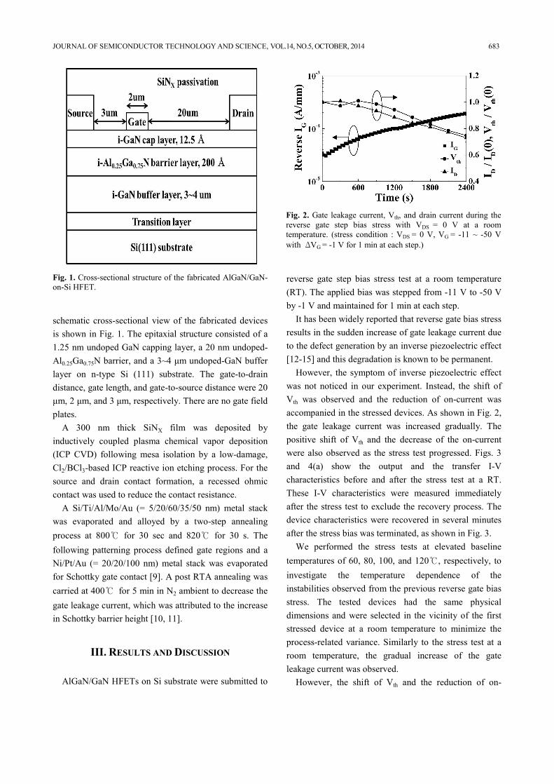
schematic cross-sectional view of the fabricated devices is shown in Fig. 1. The epitaxial structure consisted of a 1.25 nm undoped GaN capping layer, a 20 nm undoped-Al0.25Ga0.75N barrier, and a 3~4 μm undoped-GaN buffer layer on n-type Si (111) substrate. The gate-to-drain distance, gate length, and gate-to-source distance were 20 μm, 2 μm, and 3 μm, respectively. There are no gate field plates.
A 300 nm thick SiNX film was deposited by inductively coupled plasma chemical vapor deposition (ICP CVD) following mesa isolation by a low-damage, Cl2/BCl3-based ICP reactive ion etching process. For the source and drain contact formation, a recessed ohmic contact was used to reduce the contact resistance.
A Si/Ti/Al/Mo/Au (= 5/20/60/35/50 nm) metal stack was evaporated and alloyed by a two-step annealing process at 800℃ for 30 sec and 820℃ for 30 s. The following patterning process defined gate regions and a Ni/Pt/Au (= 20/20/100 nm) metal stack was evaporated for Schottky gate contact [9]. A post RTA annealing was carried at 400℃ for 5 min in N2 ambient to decrease the gate leakage current, which was attributed to the increase in Schottky barrier height [10, 11].
III. RESULTS AND DISCUSSION
AlGaN/GaN HFETs on Si substrate were submitted to
reverse gate step bias stress test at a room temperature (RT). The applied bias was stepped from -11 V to -50 V by -1 V and maintained for 1 min at each step.
It has been widely reported that reverse gate bias stress results in the sudden increase of gate leakage current due to the defect generation by an inverse piezoelectric effect [12-15] and this degradation is known to be permanent.
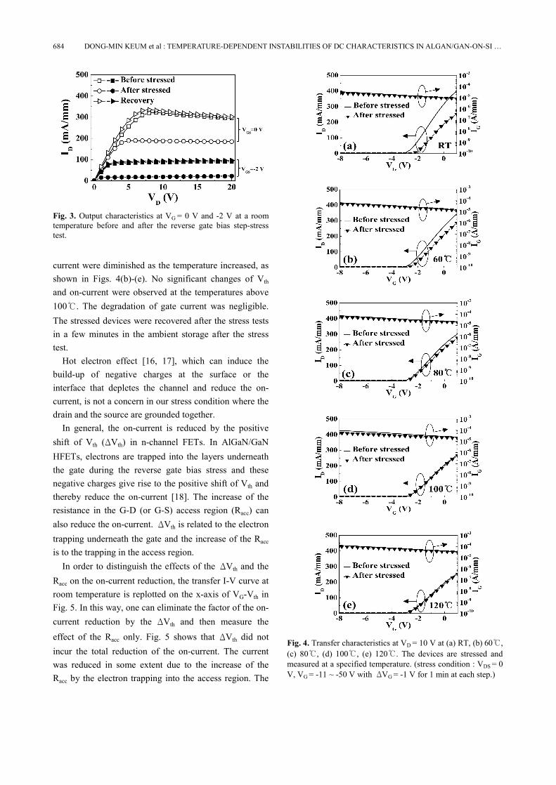
However, the symptom of inverse piezoelectric effect was not noticed in our experiment. Instead, the shift of Vth was observed and the reduction of on-current was accompanied in the stressed devices. As shown in Fig. 2, the gate leakage current was increased gradually. The positive shift of Vth and the decrease of the on-current were also observed as the stress test progressed. Figs. 3 and 4(a) show the output and the transfer I-V characteristics before and after the stress test at a RT. These I-V characteristics were measured immediately after the stress test to exclude the recovery process. The device characteristics were recovered in several minutes after the stress bias was terminated, as shown in Fig. 3.
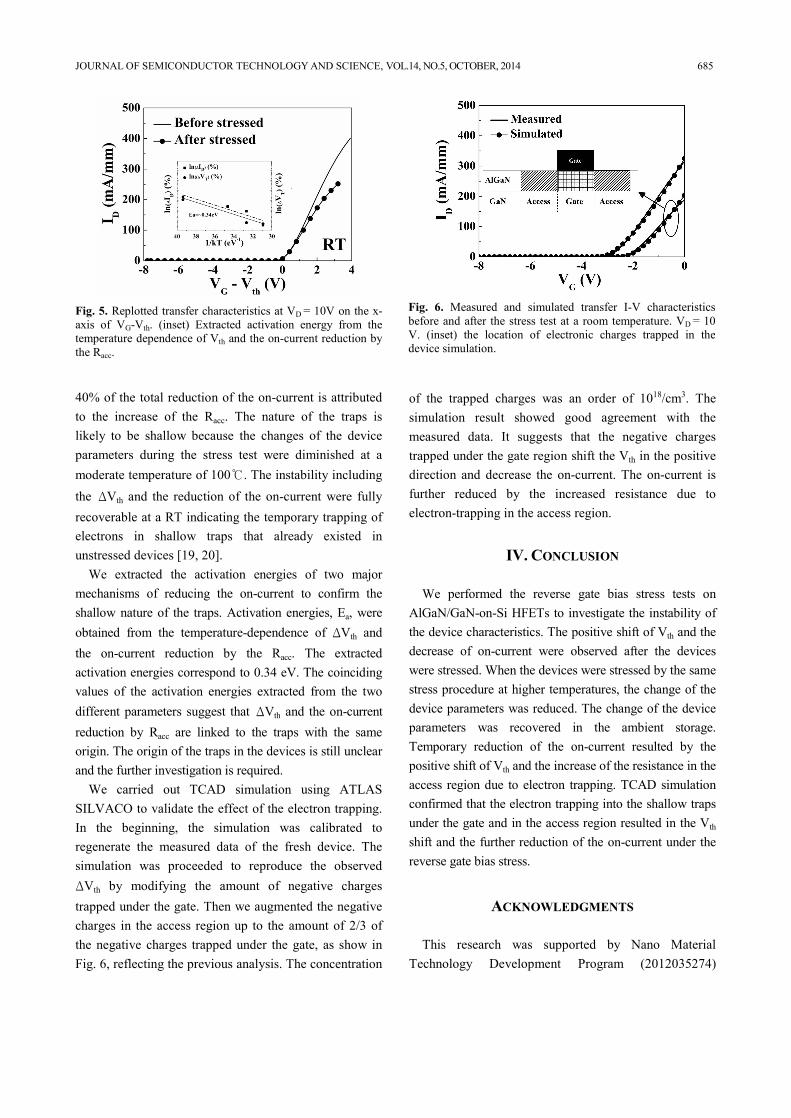
We performed the stress tests at elevated baseline temperatures of 60, 80, 100, and 120℃, respectively, to investigate the temperature dependence of the instabilities observed from the previous reverse gate bias stress. The tested devices had the same physical dimensions and were selected in the vicinity of the first stressed device at a room temperature to minimize the process-related variance. Similarly to the stress test at a room temperature, the gradual increase of the gate leakage current was observed.
However, the shift of Vth and the reduction of on-
Fig. 1. Cross-sectional structure of the fabricated AlGaN/GaN-on-Si HFET.
Fig. 2. Gate leakage current, Vth, and drain current during the reverse gate step bias stress with VDS = 0 V at a room temperature. (stress condition : VDS = 0 V, VG = -11 ~ -50 V with ΔVG = -1 V for 1 min at each step.)
684 DONG-MIN KEUM et al : TEMPERATURE-DEPENDENT INSTABILITIES OF DC CHARACTERISTICS IN ALGAN/GAN-ON-SI …
current were diminished as the temperature increased, as shown in Figs. 4(b)-(e). No significant changes of Vth and on-current were observed at the temperatures above 100℃. The degradation of gate current was negligible. The stressed devices were recovered after the stress tests in a few minutes in the ambient storage after the stress test.
Hot electron effect [16, 17], which can induce the build-up of negative charges at the surface or the interface that depletes the channel and reduce the on-current, is not a concern in our stress condition where the drain and the source are grounded together.
In general, the on-current is reduced by the positive shift of Vth (ΔVth) in n-channel FETs. In AlGaN/GaN HFETs, electrons are trapped into the layers underneath the gate during the reverse gate bias stress and these negative charges give rise to the positive shift of Vth and thereby reduce the on-current [18]. The increase of the resistance in the G-D (or G-S) access region (Racc) can also reduce the on-current. ΔVth is related to the electron trapping underneath the gate and the increase of the Racc is to the trapping in the access region.
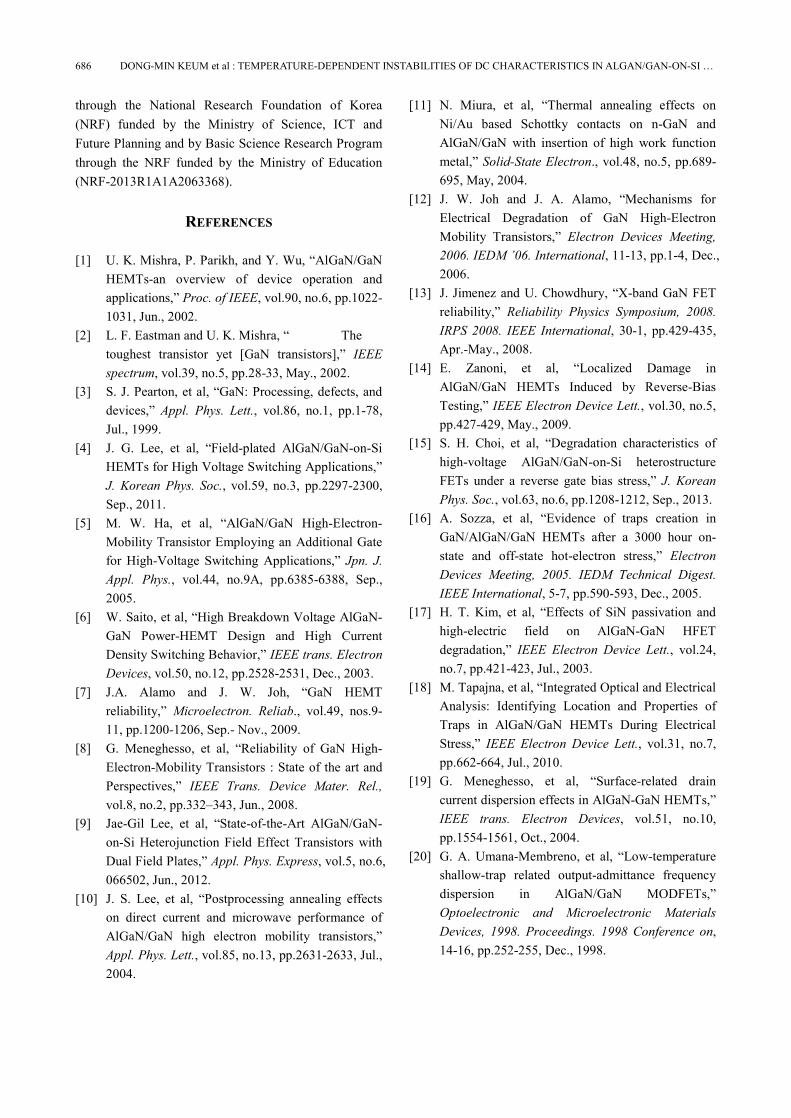
In order to distinguish the effects of the ΔVth and the Racc on the on-current reduction, the transfer I-V curve at room temperature is replotted on the x-axis of VG-Vth in Fig. 5. In this way, one can eliminate the factor of the on-current reduction by the ΔVth and then measure the effect of the Racc only. Fig. 5 shows that ΔVth did not incur the total reduction of the on-current. The current was reduced in some extent due to the increase of the Racc by the electron trapping into the access region. The
Fig. 3. Output characteristics at VG = 0 V and -2 V at a room temperature before and after the reverse gate bias step-stress test.
Fig. 4. Transfer characteristics at VD = 10 V at (a) RT, (b) 60℃, (c) 80℃, (d) 100℃, (e) 120℃. The devices are stressed and measured at a specified temperature. (stress condition : VDS = 0 V, VG = -11 ~ -50 V with ΔVG = -1 V for 1 min at each step.)
JOURNAL OF SEMICONDUCTOR TECHNOLOGY AND SCIENCE, VOL.14, NO.5, OCTOBER, 2014 685
40% of the total reduction of the on-current is attributed to the increase of the Racc. The nature of the traps is likely to be shallow because the changes of the device parameters during the stress test were diminished at a moderate temperature of 100℃. The instability including the ΔVth and the reduction of the on-current were fully recoverable at a RT indicating the temporary trapping of electrons in shallow traps that already existed in unstressed devices [19, 20].
We extracted the activation energies of two major mechanisms of reducing the on-current to confirm the shallow nature of the traps. Activation energies, Ea, were obtained from the temperature-dependence of ΔVth and the on-current reduction by the Racc. The extracted activation energies correspond to 0.34 eV. The coinciding values of the activation energies extracted from the two different parameters suggest that ΔVth and the on-current reduction by Racc are linked to the traps with the same origin. The origin of the traps in the devices is still unclear and the further investigation is required.
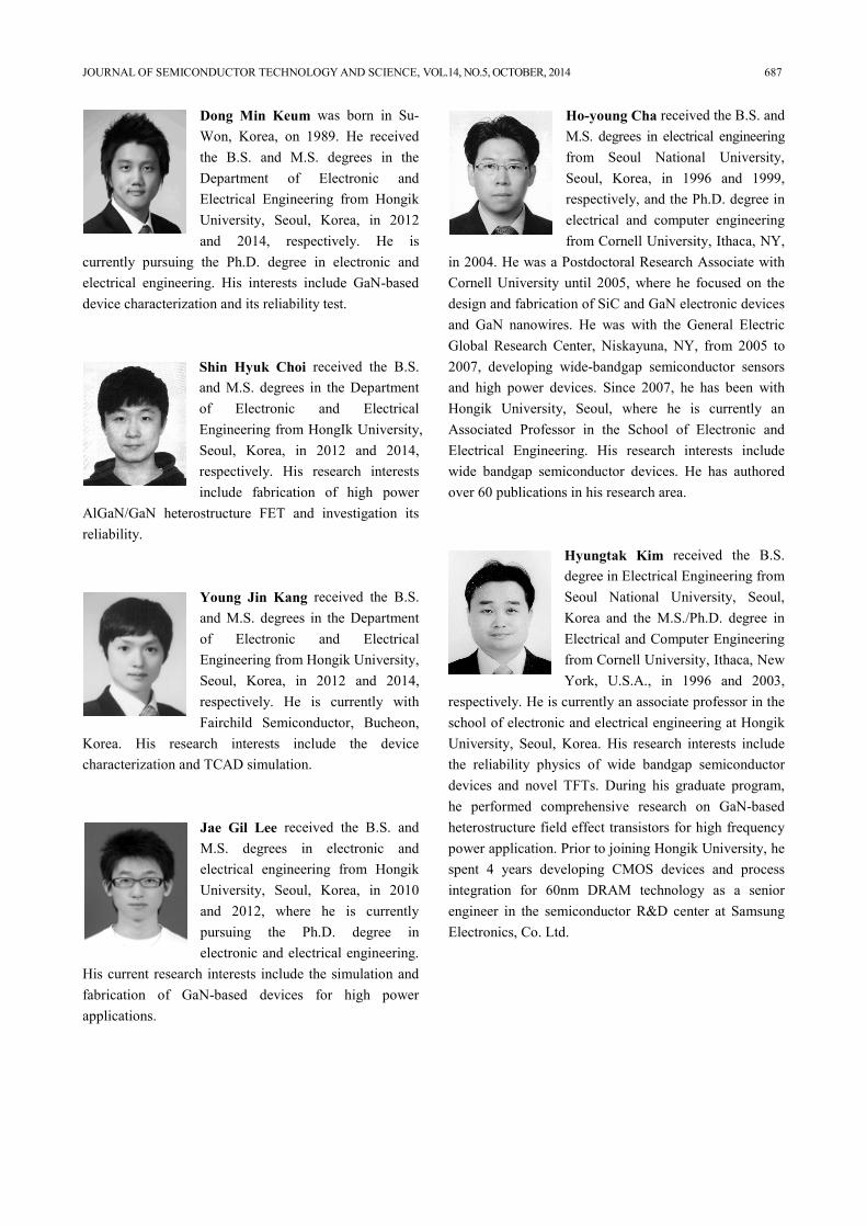
We carried out TCAD simulation using ATLAS SILVACO to validate the effect of the electron trapping. In the beginning, the simulation was calibrated to regenerate the measured data of the fresh device. The simulation was proceeded to reproduce the observed ΔVth by modifying the amount of negative charges trapped under the gate. Then we augmented the negative charges in the access region up to the amount of 2/3 of the negative charges trapped under the gate, as show in Fig. 6, reflecting the previous analysis. The concentration
of the trapped charges was an order of 1018/cm3. The simulation result showed good agreement with the measured data. It suggests that the negative charges trapped under the gate region shift the Vth in the positive direction and decrease the on-current. The on-current is further reduced by the increased resistance due to electron-trapping in the access region.
IV. CONCLUSION
We performed the reverse gate bias stress tests on AlGaN/GaN-on-Si HFETs to investigate the instability of the device characteristics. The positive shift of Vth and the decrease of on-current were observed after the devices were stressed. When the devices were stressed by the same stress procedure at higher temperatures, the change of the device parameters was reduced. The change of the device parameters was recovered in the ambient storage. Temporary reduction of the on-current resulted by the positive shift of Vth and the increase of the resistance in the access region due to electron trapping. TCAD simulation confirmed that the electron trapping into the shallow traps under the gate and in the access region resulted in the Vth shift and the further reduction of the on-current under the reverse gate bias stress.
ACKNOWLEDGMENTS
This research was supported by Nano Material Technology Development Program (2012035274)
Fig. 5. Replotted transfer characteristics at VD = 10V on the x-axis of VG-Vth. (inset) Extracted activation energy from the temperature dependence of Vth and the on-current reduction by the Racc.
Fig. 6. Measured and simulated transfer I-V characteristics before and after the stress test at a room temperature. VD = 10V. (inset) the location of electronic charges trapped in the device simulation.
686 DONG-MIN KEUM et al : TEMPERATURE-DEPENDENT INSTABILITIES OF DC CHARACTERISTICS IN ALGAN/GAN-ON-SI …
through the National Research Foundation of Korea (NRF) funded by the Ministry of Science, ICT and Future Planning and by Basic Science Research Program through the NRF funded by the Ministry of Education (NRF-2013R1A1A2063368).
REFERENCES
[1] U. K. Mishra, P. Parikh, and Y. Wu, “AlGaN/GaN HEMTs-an overview of device operation and applications,” Proc. of IEEE, vol.90, no.6, pp.1022-1031, Jun., 2002.
[2] L. F. Eastman and U. K. Mishra, “ The toughest transistor yet [GaN transistors],” IEEE spectrum, vol.39, no.5, pp.28-33, May., 2002.
[3] S. J. Pearton, et al, “GaN: Processing, defects, and devices,” Appl. Phys. Lett., vol.86, no.1, pp.1-78, Jul., 1999.
[4] J. G. Lee, et al, “Field-plated AlGaN/GaN-on-Si HEMTs for High Voltage Switching Applications,” J. Korean Phys. Soc., vol.59, no.3, pp.2297-2300, Sep., 2011.
[5] M. W. Ha, et al, “AlGaN/GaN High-Electron-Mobility Transistor Employing an Additional Gate for High-Voltage Switching Applications,” Jpn. J. Appl. Phys., vol.44, no.9A, pp.6385-6388, Sep., 2005.
[6] W. Saito, et al, “High Breakdown Voltage AlGaN-GaN Power-HEMT Design and High Current Density Switching Behavior,” IEEE trans. Electron Devices, vol.50, no.12, pp.2528-2531, Dec., 2003.
[7] J.A. Alamo and J. W. Joh, “GaN HEMT reliability,” Microelectron. Reliab., vol.49, nos.9-11, pp.1200-1206, Sep.- Nov., 2009.
[8] G. Meneghesso, et al, “Reliability of GaN High-Electron-Mobility Transistors : State of the art and Perspectives,” IEEE Trans. Device Mater. Rel., vol.8, no.2, pp.332–343, Jun., 2008.
[9] Jae-Gil Lee, et al, “State-of-the-Art AlGaN/GaN-on-Si Heterojunction Field Effect Transistors with Dual Field Plates,” Appl. Phys. Express, vol.5, no.6, 066502, Jun., 2012.
[10] J. S. Lee, et al, “Postprocessing annealing effects on direct current and microwave performance of AlGaN/GaN high electron mobility transistors,” Appl. Phys. Lett., vol.85, no.13, pp.2631-2633, Jul., 2004.
[11] N. Miura, et al, “Thermal annealing effects on Ni/Au based Schottky contacts on n-GaN and AlGaN/GaN with insertion of high work function metal,” Solid-State Electron., vol.48, no.5, pp.689-695, May, 2004.
[12] J. W. Joh and J. A. Alamo, “Mechanisms for Electrical Degradation of GaN High-Electron Mobility Transistors,” Electron Devices Meeting, 2006. IEDM ’06. International, 11-13, pp.1-4, Dec., 2006.
[13] J. Jimenez and U. Chowdhury, “X-band GaN FET reliability,” Reliability Physics Symposium, 2008. IRPS 2008. IEEE International, 30-1, pp.429-435, Apr.-May., 2008.
[14] E. Zanoni, et al, “Localized Damage in AlGaN/GaN HEMTs Induced by Reverse-Bias Testing,” IEEE Electron Device Lett., vol.30, no.5, pp.427-429, May., 2009.
[15] S. H. Choi, et al, “Degradation characteristics of high-voltage AlGaN/GaN-on-Si heterostructure FETs under a reverse gate bias stress,” J. Korean Phys. Soc., vol.63, no.6, pp.1208-1212, Sep., 2013.
[16] A. Sozza, et al, “Evidence of traps creation in GaN/AlGaN/GaN HEMTs after a 3000 hour on-state and off-state hot-electron stress,” Electron Devices Meeting, 2005. IEDM Technical Digest. IEEE International, 5-7, pp.590-593, Dec., 2005.
[17] H. T. Kim, et al, “Effects of SiN passivation and high-electric field on AlGaN-GaN HFET degradation,” IEEE Electron Device Lett., vol.24, no.7, pp.421-423, Jul., 2003.
[18] M. Tapajna, et al, “Integrated Optical and Electrical Analysis: Identifying Location and Properties of Traps in AlGaN/GaN HEMTs During Electrical Stress,” IEEE Electron Device Lett., vol.31, no.7, pp.662-664, Jul., 2010.
[19] G. Meneghesso, et al, “Surface-related drain current dispersion effects in AlGaN-GaN HEMTs,” IEEE trans. Electron Devices, vol.51, no.10, pp.1554-1561, Oct., 2004.
[20] G. A. Umana-Membreno, et al, “Low-temperature shallow-trap related output-admittance frequency dispersion in AlGaN/GaN MODFETs,” Optoelectronic and Microelectronic Materials Devices, 1998. Proceedings. 1998 Conference on, 14-16, pp.252-255, Dec., 1998.
JOURNAL OF SEMICONDUCTOR TECHNOLOGY AND SCIENCE, VOL.14, NO.5, OCTOBER, 2014 687
Dong Min Keum was born in Su-Won, Korea, on 1989. He received the B.S. and M.S. degrees in the Department of Electronic and Electrical Engineering from Hongik University, Seoul, Korea, in 2012 and 2014, respectively. He is
currently pursuing the Ph.D. degree in electronic and electrical engineering. His interests include GaN-based device characterization and its reliability test.
Shin Hyuk Choi received the B.S. and M.S. degrees in the Department of Electronic and Electrical Engineering from HongIk University, Seoul, Korea, in 2012 and 2014, respectively. His research interests include fabrication of high power
AlGaN/GaN heterostructure FET and investigation its reliability.
Young Jin Kang received the B.S. and M.S. degrees in the Department of Electronic and Electrical Engineering from Hongik University, Seoul, Korea, in 2012 and 2014, respectively. He is currently with Fairchild Semiconductor, Bucheon,
Korea. His research interests include the device characterization and TCAD simulation.
Jae Gil Lee received the B.S. and M.S. degrees in electronic and electrical engineering from Hongik University, Seoul, Korea, in 2010 and 2012, where he is currently pursuing the Ph.D. degree in electronic and electrical engineering.
His current research interests include the simulation and fabrication of GaN-based devices for high power applications.
Ho-young Cha received the B.S. and M.S. degrees in electrical engineering from Seoul National University, Seoul, Korea, in 1996 and 1999, respectively, and the Ph.D. degree in electrical and computer engineering from Cornell University, Ithaca, NY,
in 2004. He was a Postdoctoral Research Associate with Cornell University until 2005, where he focused on the design and fabrication of SiC and GaN electronic devices and GaN nanowires. He was with the General Electric Global Research Center, Niskayuna, NY, from 2005 to 2007, developing wide-bandgap semiconductor sensors and high power devices. Since 2007, he has been with Hongik University, Seoul, where he is currently an Associated Professor in the School of Electronic and Electrical Engineering. His research interests include wide bandgap semiconductor devices. He has authored over 60 publications in his research area.
Hyungtak Kim received the B.S. degree in Electrical Engineering from Seoul National University, Seoul, Korea and the M.S./Ph.D. degree in Electrical and Computer Engineering from Cornell University, Ithaca, New York, U.S.A., in 1996 and 2003,
respectively. He is currently an associate professor in the school of electronic and electrical engineering at Hongik University, Seoul, Korea. His research interests include the reliability physics of wide bandgap semiconductor devices and novel TFTs. During his graduate program, he performed comprehensive research on GaN-based heterostructure field effect transistors for high frequency power application. Prior to joining Hongik University, he spent 4 years developing CMOS devices and process integration for 60nm DRAM technology as a senior engineer in the semiconductor R&D center at Samsung Electronics, Co. Ltd.