Thermal Characterization of Individual Pixels in...
6
JOURNAL OF SEMICONDUCTOR TECHNOLOGY AND SCIENCE, VOL.15, NO.5, OCTOBER, 2015 ISSN(Print) 1598-1657 http://dx.doi.org/10.5573/JSTS.2015.15.5.533 ISSN(Online) 2233-4866 Manuscript received Apr. 21, 2015; accepted Sep. 21, 2015 1 Division of Scientific Instrumentation, Korea Basic Science Institute, 169-148 Gwahak-ro, Yuseong-gu, Daejeon 305-806, Republic of Korea. 2 National NanoFab Center, 291 Gwahak-ro, Yuseong-gu, Daejeon 305-701, Republic of Korea. 3 Daegu-Gyeongbuk Medical Innovation Foundation, 88 Dongnae-ro, Dong-gu, Daegu 701-310, Republic of Korea E-mail : [email protected] Thermal Characterization of Individual Pixels in Microbolometer Image Sensors by Thermoreflectance Microscopy Seon Young Ryu 1 , Hae Young Choi 1, 3 , Dong Uk Kim 1 , Geon Hee Kim 1 , Taehyun Kim 2 , Hee Yeoun Kim 2 , and Ki Soo Chang 1,* Abstract—Thermal characterization of individual pixels in microbolometer infrared image sensors is needed for optimal design and improved performance. In this work, we used thermoreflectance microscopy on uncooled microbolometer image sensors to investigate the thermal characteristics of individual pixels. Two types of microbolometer image sensors with a shared-anchor structure were fabricated and thermally characterized at various biases and vacuum levels by measuring the temperature distribution on the surface of the microbolometers. The results show that thermoreflectance microscopy can be a useful thermal characterization tool for microbolometer image sensors. Index Terms—Microbolometer, infrared image sensor, thermoreflectance microscopy, thermal characterization I. INTRODUCTION The microbolometer image sensor is a type of thermal image sensor in which the thermal infrared radiation from an object is absorbed on the surface of the microbolometer detector, and the resultant temperature rise of the detector, corresponding to the amount of absorbed infrared energy, is measured by a readout circuit as a change of microbolometer resistance. These sensors have become a technology of choice in both military and commercial applications due to their small size, minimal power consumption, and low cost [1-3]. High-end commercial applications in the automotive, security, and medical fields require large format arrays; this in turn necessitates a reduction in pixel size for weight reduction, system size, low cost, and resolution enhancement. However, downsizing of the micro- bolometer pixels produces a dramatic drop in sensitivity. The performance of microbolometer image sensors is driven by the thermal characteristics of the individual pixels [4]. Therefore, optimized bolometer design and precise thermal analysis of individual pixels on image sensors are required to improve the thermal properties as the pixel size is reduced. In general, the thermal behavior of a microbolometer detector can be evaluated by the electro-thermal analogy [2, 5]. The electrical and thermal properties of a single pixel of a microbolometer array can be estimated through the measurement of electrical resistance, but it is difficult to measure thermal distribution over the active area. Although the two-dimensional (2-D) thermal modeling of a microbolometer can be accomplished with simulation tools such as ANSYS and CoventorWare [6, 7], precise parameter setting and iterative calculations are indispensable to obtain the correlation factors for reliable results. Recently, a long-wave infrared (LWIR) microscope has been used for thermal characterization of
Transcript of Thermal Characterization of Individual Pixels in...
JOURNAL OF SEMICONDUCTOR TECHNOLOGY AND SCIENCE, VOL.15, NO.5, OCTOBER, 2015 ISSN(Print) 1598-1657 http://dx.doi.org/10.5573/JSTS.2015.15.5.533 ISSN(Online) 2233-4866
Manuscript received Apr. 21, 2015; accepted Sep. 21, 2015 1 Division of Scientific Instrumentation, Korea Basic Science Institute, 169-148 Gwahak-ro, Yuseong-gu, Daejeon 305-806, Republic of Korea. 2 National NanoFab Center, 291 Gwahak-ro, Yuseong-gu, Daejeon 305-701, Republic of Korea. 3 Daegu-Gyeongbuk Medical Innovation Foundation, 88 Dongnae-ro, Dong-gu, Daegu 701-310, Republic of Korea E-mail : [email protected]
Thermal Characterization of Individual Pixels in Microbolometer Image Sensors by Thermoreflectance
Microscopy
Seon Young Ryu1, Hae Young Choi1, 3, Dong Uk Kim1, Geon Hee Kim1, Taehyun Kim2, Hee Yeoun Kim2, and Ki Soo Chang1,*
Abstract—Thermal characterization of individual pixels in microbolometer infrared image sensors is needed for optimal design and improved performance. In this work, we used thermoreflectance microscopy on uncooled microbolometer image sensors to investigate the thermal characteristics of individual pixels. Two types of microbolometer image sensors with a shared-anchor structure were fabricated and thermally characterized at various biases and vacuum levels by measuring the temperature distribution on the surface of the microbolometers. The results show that thermoreflectance microscopy can be a useful thermal characterization tool for microbolometer image sensors. Index Terms—Microbolometer, infrared image sensor, thermoreflectance microscopy, thermal characterization
I. INTRODUCTION
The microbolometer image sensor is a type of thermal image sensor in which the thermal infrared radiation from an object is absorbed on the surface of the microbolometer detector, and the resultant temperature
rise of the detector, corresponding to the amount of absorbed infrared energy, is measured by a readout circuit as a change of microbolometer resistance. These sensors have become a technology of choice in both military and commercial applications due to their small size, minimal power consumption, and low cost [1-3]. High-end commercial applications in the automotive, security, and medical fields require large format arrays; this in turn necessitates a reduction in pixel size for weight reduction, system size, low cost, and resolution enhancement. However, downsizing of the micro- bolometer pixels produces a dramatic drop in sensitivity. The performance of microbolometer image sensors is driven by the thermal characteristics of the individual pixels [4]. Therefore, optimized bolometer design and precise thermal analysis of individual pixels on image sensors are required to improve the thermal properties as the pixel size is reduced.
In general, the thermal behavior of a microbolometer detector can be evaluated by the electro-thermal analogy [2, 5]. The electrical and thermal properties of a single pixel of a microbolometer array can be estimated through the measurement of electrical resistance, but it is difficult to measure thermal distribution over the active area. Although the two-dimensional (2-D) thermal modeling of a microbolometer can be accomplished with simulation tools such as ANSYS and CoventorWare [6, 7], precise parameter setting and iterative calculations are indispensable to obtain the correlation factors for reliable results. Recently, a long-wave infrared (LWIR) microscope has been used for thermal characterization of

534 SEON YOUNG RYU et al : THERMAL CHARACTERIZATION OF INDIVIDUAL PIXELS IN MICROBOLOMETER IMAGE …
a microbolometer array [8]. However, this approach provides only an average temperature of the detector array, but not actual thermal information on individual bolometer pixels. Moreover, this approach requires an additional fill factor correction due to the limited spatial resolution and field of view of the LWIR camera.
In this paper, we demonstrate, for the first time, thermal imaging and characterization of individual pixels in microbolometer image sensors using thermore- flectance microscopy (TRM), a contactless optical imaging technique that provides a 2-D thermal image of semiconductor devices with high spatial and thermal resolution [9-11]. Two types of custom-designed microbolometers with a shared-anchor structure were prepared, and the thermal properties of both were quantitatively measured at various bias and vacuum conditions by self-heating of the active area.
II. MATERIALS AND METHODS
Fig. 1 shows a schematic of the TRM system based on a conventional microscope head (FS70, Mitutoyo) integrated with a blue light-emitting diode (λ=473 nm), a 14-bit CCD camera (1600´1200, 30 Hz), and a microscope objective (100´, 0.7 NA). The probe beam illuminated a vacuum-packaged microbolometer surface and the reflected light was measured by a visible CCD camera. The 2-D self-heating images were acquired by measuring the temperature-dependent reflectivity change distribution on the microbolometer surface with bias voltage modulation. The bias modulation was phase-locked to the CCD frame triggered at four times the bias
modulation frequency for the lock-in detection of the reflectivity change distribution. The CCD triggering signal was supplied by analog output signal from the data acquisition (DAQ) board (NI PCIe-6353, National Instruments). Each pixel on the microbolometer array was electrically controlled by a SaFPA™ (Semi-Active Focal Plane Array) measurement circuit [12]. The system control and image-processing program was written in the LABVIEW programming environment. A spatial resolution about 0.5μm can be achieved with a 100´ objective lens with 0.7 NA [10, 11].
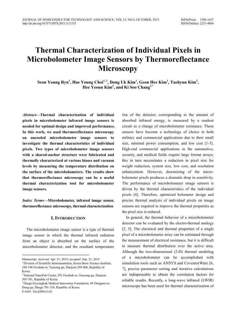
As test samples, we prepared two types of microbolometer image sensors, both based on amorphous Si. Both types had a shared-anchor structure designed to enhance the fill factor, as shown in Fig. 2(a) and (b); they will be referred to as design1 and design2, respectively. Generally, the microbolometer pixels are designed to suppress the heat loss by the thermal conduction through the support structure (anchor and leg) of suspended membrane, which provides mechanical support, thermal conduction path, and electrical conduction path. To obtain high performance microbolometer sensors, the support structure should be optimized. Microbolometer design1 and design2 effectively have one anchor per unit pixel by sharing the anchor with neighboring pixels. The difference between microbolometer design1 and design2 is the support structure. Design1 has two anchors around unit pixel and one anchor is shared by two pixels, located diagonal direction. Design2 has four anchors around unit pixel and one anchor is shared by four neighboring pixels. The mechanical simulation results and fabrication processes for design1 and design2 have been described elsewhere [12]. As shown in Fig. 3, the fabricated
Fig. 1. Schematic of the thermoreflectance microscopy system
Fig. 2. Shared-anchor microbolometer, (a) design1, (b) design2. Black line: leg for mechanical support of suspended membrane, red line: leg for electrical conduction. Inset: unit pixel structure
JOURNAL OF SEMICONDUCTOR TECHNOLOGY AND SCIENCE, VOL.15, NO.5, OCTOBER, 2015 535
microbolometer arrays were vacuum packaged with a zinc sulfide (ZnS) window that was transparent from the visible range to the far infrared (0.4 to 12μm) for both TRM imaging at visible wavelength range and thermal sensing with the bolometer array itself in the long-wavelength infrared range. The measured fill factors of design1 and design2 were 73% and 62%, respectively. These fill factors are significantly higher than that of the conventional unshared-anchor design (fill factor 53%).
III. RESULTS AND DISCUSSION
The temperature increment (T-To) due to the self-heating effect can be estimated from the electro-thermal analogy with the following formula [2]
2
( )o th inRIT T R PG
- = = (1)
where I and R are applied current and electrical resistance respectively of a microbolometer pixel, G is the thermal conductance, Rth is the thermal resistance and Pin is the applied power. The thermal resistance can be calculated by measuring the inverse of the resistance as a function of I2 according to the following relation
21 1th
oR I
R Ra= - (2)
where Ro is the resistance at the temperature To and a is the temperature coefficient of resistance (TCR), which was experimentally determined to be 2.3%. By measuring the inverse of the resistance as a function of I2 according to Eq. (2), the thermal resistance (Rth) can be
found by linear curve fitting. The extracted thermal resistances of design1 and design2 were 6.8 and 11.5 K/mW, respectively, under a vacuum level of 2´10-5 torr. The corresponding temperature increments estimated by electro-thermal analogy with Eq. (1) were 6.7 K and 11.4 K, respectively, at 1 V bias.
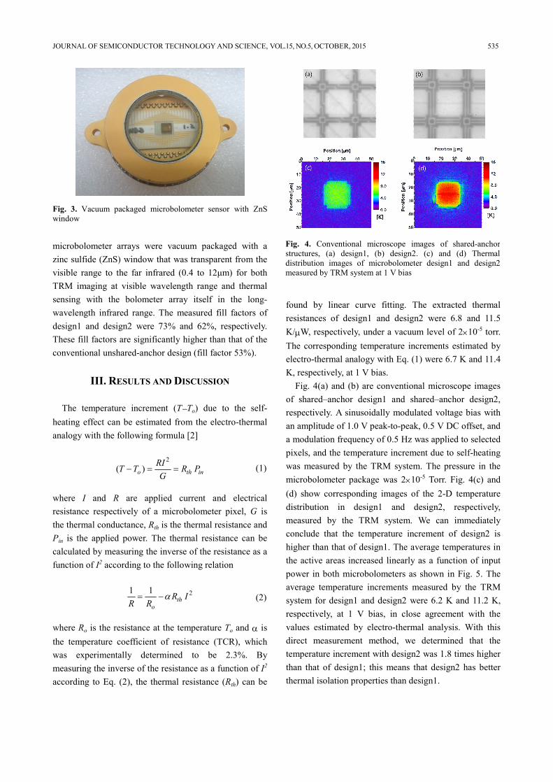
Fig. 4(a) and (b) are conventional microscope images of shared–anchor design1 and shared–anchor design2, respectively. A sinusoidally modulated voltage bias with an amplitude of 1.0 V peak-to-peak, 0.5 V DC offset, and a modulation frequency of 0.5 Hz was applied to selected pixels, and the temperature increment due to self-heating was measured by the TRM system. The pressure in the microbolometer package was 2´10-5 Torr. Fig. 4(c) and (d) show corresponding images of the 2-D temperature distribution in design1 and design2, respectively, measured by the TRM system. We can immediately conclude that the temperature increment of design2 is higher than that of design1. The average temperatures in the active areas increased linearly as a function of input power in both microbolometers as shown in Fig. 5. The average temperature increments measured by the TRM system for design1 and design2 were 6.2 K and 11.2 K, respectively, at 1 V bias, in close agreement with the values estimated by electro-thermal analysis. With this direct measurement method, we determined that the temperature increment with design2 was 1.8 times higher than that of design1; this means that design2 has better thermal isolation properties than design1.
Fig. 3. Vacuum packaged microbolometer sensor with ZnS window
Fig. 4. Conventional microscope images of shared-anchor structures, (a) design1, (b) design2. (c) and (d) Thermal distribution images of microbolometer design1 and design2 measured by TRM system at 1 V bias

536 SEON YOUNG RYU et al : THERMAL CHARACTERIZATION OF INDIVIDUAL PIXELS IN MICROBOLOMETER IMAGE …
In the case of uncooled microbolometer detectors, vacuum packaging is critical to maximize the thermal isolation, and ensure good responsivity [13]. In this work, we measured the thermal distribution images under various pressures to investigate the dependence of the thermal isolation properties on pressure. Fig. 6 presents the pressure dependence of temperature distribution for the selected microbolometer pixel design2 at 1 V bias. Fig. 7 shows average temperature variations in the active area as a function of pressure, and Fig. 6(a) to (d) show corresponding thermal distribution images at pressures of (a) 10-5, (b) 10-3, (c) 10-1 and (d) 10 Torr. The temperature increase (ΔT), which represents the amount of thermal isolation, maintained nearly the same value until the pressure reached about 10-2 Torr, and then started to drop due to heat loss by convection. From the quantitative
experimental measurements of the pressure dependence of thermal isolation, we can directly estimate the packaging performance of the microbolometer image sensors after vacuum sealing.
IV. CONCLUSIONS
We experimentally demonstrated the thermal characteristics of individual pixels in microbolometer image sensors by use of a thermoreflectance microscopy technique. The 2-D temperature distribution on the pixels of two types of shared-anchor structured microbolometers was quantitatively measured. The measured thermal characteristics agreed closely with the results extracted by electro-thermal analysis. We also evaluated the pressure dependence of the thermal isolation charac- teristics of microbolometer sensors by measuring the quantitative thermal distribution images as a function of pressure. The results demonstrate that thermoreflectance microscopy is a useful tool to estimate the thermal properties of microbolometer pixels for optimal bolometer design and performance enhancement.
ACKNOWLEDGMENTS
This work was supported by the Korea Basic Science Institute grant (C35936 & D35500), National Research Council of Science & Technology grant (PBE083), and Daedeok Technology Business Program (Announcement 2011-343) funded by MKE (Ministry of Knowledge Economy).
Fig. 5. Measured temperature variations of microbolometer design1 and design2 as a function of input power
Fig. 6. Thermal distribution images of microbolometer design2 measured by the TRM system at vacuum levels of (a) 10-5, (b) 10-3, (c) 10-1, (d) 10 Torr
Fig. 7. Average temperature variation of microbolometer design1 and design 2 as a function of pressure measured by TRM system

JOURNAL OF SEMICONDUCTOR TECHNOLOGY AND SCIENCE, VOL.15, NO.5, OCTOBER, 2015 537
REFERENCES
[1] J. L. Tissot, “IR detection with uncooled focal plane arrays. State of the art and trends,” Opto-Electron. Rev., vol. 12, no. 1, pp.105-109, 2004.
[2] R. K. Bhan, R. S. Saxena, C. R. Jalwania, and S. K. Lomash, “Uncooled Infrared Microbolometer Arrays and their Characterisation Techniques,” Def. Sci. J., vol. 59, no. 6, pp.580-589, 2009.
[3] F. Niklaus, C. Vieider, and H. Jakobsen, “MEMS-based uncooled infrared bolometer arrays – A Review,” Proc. of SPIE vol. 6836, p.68360D, 2007.
[4] J. J. Yon, E. Mottin, and J. L. Tissot, “Latest amorphous silicon microbolometer developments at LETI-LIR,” Proc. of SPIE vol. 6940, p.69401W, 2008.
[5] P. Eriksson, J. Y. Andersson, and G. Stemme, “Thermal characterization of surface-micromachined silicon nitride membranes for thermal infrared detectors,” J. Microelectromech. Syst., vol. 6, no. 1, pp. 55-61, 1997.
[6] A. J. Syllaios, Miranda J. Ha, William L. McCardel, Thomas R. Schimert, “Measurement of thermal time constant of microbolometer arrays,” Proc. of SPIE vol.5783, pp. 625-630, 2005.
[7] S. Han, C. H. Chun, C. S. Han and S. M. Park, “Parameterized simulation program with integrated circuit emphasis modeling of two-level micro- bolometer,” J. of Electr. Eng. Technol., vol. 6, no. 2, pp. 270-274, 2011.
[8] G. Bieszczad and M. Kastek, “Measurement of thermal behavior of detector array surface with the use of microscopic thermal camera,” Metrol. Meas. Syst. vol. 18, no. 4, pp. 679-690, 2011.
[9] M. Farzaneh, K. Maize, D. Lüerßen, J. A. Summers, P. M. Mayer, P. E. Raad, K. P. Pipe, A. Shakouri, R. J. Ram, J. A. Hudgings, “CCD-based thermor- eflectance microscopy: principles and applications,” J. Phys. D: Appl. Phys. vol. 42, p. 143001, 2009.
[10] S. Y. Ryu, D. U. Kim, J. K. Kim, H. Y. Choi, G. H. Kim and K. S. Chang, “Surface temperature measurement and submicron defect isolation for microelectronic devices using thermoreflectance microscopy”, Int. J. Thermophys., online first, 2014.
[11] J. I. Kim, K. S. Chang, D. U. Kim, I.-T. Cho, C.-Y. Jeong, D. Lee, H.-I. Kwon, S. Jin, and J.-H. Lee, “Thermoreflectance microscopy analysis on self-
heating effect of short-channel amorphous In-Ga-Zn-O thin film transistors”, Appl. Phys. Lett., vol. 105, p. 043501, 2014.
[12] T. Kim, K. Kyung, J. H. Park, Y. S. Kim, S. K. Lim, K. Kim, K. Lee, H. Y. Kim, C. Welham, “Development of microbolometer with high fill factor and high mechanical stability by shared-anchor structure,” Proc. of SPIE, vol. 8353, p. 83531B, 2012.
[13] S. Garcia-Blanco, P. Topart, Y. Desroches, J.S. Caron, F. Williamson, C. Alain, H. Jerominek, “Low-temperature vacuum hermetic wafer-level package for uncooled microbolometer FPAs,” Proc. of SPIE, vol. 6884, p.68840P, 2008.
Seon Young Ryu received the B.S. and M.S. degrees in physics from Chungbuk National University, Chungbuk, Korea, in 1999 and 2002, respectively, another M.S. degree and Ph.D. degree from the Gwangju
Institute of Science and Technology, Gwangju, Korea, in 2005 and 2010, respectively. After working as a researcher at the Division of Instrument Development, Korea Basic Science Institute in Korea from 2010 to 2013, she joined Green Optics Co., Ltd. as a senior researcher. Her research interests include optical devices and optical imaging systems.
Hae Young Choi received the B.S. degree in physics from Chungbuk National University, Chungbuk, Korea, in 2001, M.S. degree and Ph.D. degree from the Gwangju Institute of Science and Technology, Gwangju, Korea, in
2005 and 2010, respectively. After working as a researcher at the Division of Instrument Development, Korea Basic Science Institute in Korea from 2010 to 2011, he jointed Osong Medical Innovation Foundation in Korea, as a researcher from 2011 to 2013. Since January 2015, he has been working at the Daegu-Gyeongbuk Medical Innovation Foundation, as a senior researcher. His current research interests are developing Medical devices and Medical imaging systems.

538 SEON YOUNG RYU et al : THERMAL CHARACTERIZATION OF INDIVIDUAL PIXELS IN MICROBOLOMETER IMAGE …
Dong Uk Kim received the B.S. degree in the school of Electrical, Electronics and Communication Engineering from Kongju National University in 2001 and the M.S. and Ph.D. degrees in the School of
Information and Mechatronics from Gwangju Institute of Science & Technology (GIST) in 2006 and 2013, respectively. Currently, He is a senior researcher in the Korea Basic Science Institute (KBSI). His current research interest is the development of the thermal imaging system for semiconductor device applications.
Geon Hee Kim received the Ph.D. degree in the Department of Mecha- nical Engineering from Chungnam National University in 2003. He joined Optical Instrumentation Devel- opment Team, Korea Basic Science
Institute (KBSI) in 1993, as a Principal Researcher. His current research interests focus on the areas of Biomechanics, Optical Devices and Ultra precision manufacturing.
Taehyun Kim received the B. S degree in department of Electronic Physics from Hankuk University of Foreign Studies. He have been worked at Korea Electronics Tech- nology Institute (KETI) studied about cell analysis by IR spectrum during
2006~2008. He have been worked assistant researcher, studied about micro-bolometer testing, analysis, and simulation at OCAS, co. during 2008~2010. Currently working on Sensor design, test, integration & packaging branch of, Nanosystem research division, National NanoFab Center (NNFC).
Hee Yeoun Kim received the B.S. degree from Hanyang University, Seoul, Korea, in 1990, the M.S. and Ph.D in department of material science and engineering from Korea Advanced Institute of Science and Technology, Taejeon, Korea, in1993,
2005, respectively. He was senior researcher at Agency for Defense Develop-ment during 1993–2000. He has developed micro-optical modulator as a principal researcher at Samsung Electromechanics Co. during 2006–2008. Currently, he is leading MEMS/NEMS research group at National NanoFab Center since 2008. His research interests are MOEMS and its reliability issues.
Ki Soo Chang received the B.S. degree in the Department of Elec- tronic Materials and Device Engi- neering from Inha University in 1999 and the M.S. and Ph.D. degrees in the Department of Information and Communications from Gwangju
Institute of Science & Technology (GIST) in 2002 and 2007, respectively. In 2007, he joined the Korea Basic Science Institute (KBSI), where he is presently a principal researcher. His current research interests are thermal imaging microscope for semiconductor device applications and nano-bio-photonic fusion imaging system for bio-medical applications.


![A Piezoelectric Energy Harvester with High Efficiency and ...jsts.org/html/journal/journal_files/2015/06/Year... · [1-5]. The first approach is to discharge the capacitor with a](https://static.fdocuments.in/doc/165x107/5f05e1827e708231d4152e99/a-piezoelectric-energy-harvester-with-high-efficiency-and-jstsorghtmljournaljournalfiles201506year.jpg)