SEMICON Taiwan 2009 - Semiconductor Equipment/Materials/Fab Outlook

dL • - - - • ^^^ ML


Introduction to the Service
•
The Semiconductor Equipment and Materials Service (SEMS) is a comprehensive, worldwide information service that documents and analyzes important aspects of the Semiconductor Equipment and Materials Industry. The service consists of:
• Two 3-inch, loose-leaf binders containing reference data base material that is continually revised and updated as developments occur or additional information becomes available
• Newsletters providing executive summaries of key industry events or significant changes in the reference material from the other binders; a
^ -newsletter binder is provided for storing this material
• Inquiry privileges for two individuals at each subscribing company; this service provides an open line to the research staff for amplification of data base and newsletter information
• An annual three-day conference with industry experts discussing developments of current interest and importance
The service analyzes and reports on the equipment and materials used in the production of semiconductors and assesses the effects of rapid industry growth, frequent and rapid industry fluctuations, technological complexity, technological innovations, short product cycles, and fierce competition. To answer questions on the industry, the service will:
• Discuss current and emerging technologies and trends, including historical and forecast market data, and market shares for each major type of equipment and materials
•
•
Provide profiles of worldwide equipment and materials companies and company financial reports
Provide a complete picture of the semiconductor industry including its — problems and trends as well as locations of semiconductor facilities and the
technologies produced at these locations
• Present current, forecast, and historical capital spending by the worldwide semiconductor industry, analyzed by company
• Provide analyses of industry wafer fabrication capacity and its effect on both the semiconductor companies and the equipment and materials companies including actual wafer starts, excess capacity, and forecasts of capacity utilization.
• Present worldwide semiconductor production, revenue/square inch of silicon, and other key ratios for the semiconductor and the equipment and materials industry
SEMS Markets and Technology © 1988 Dataquest Incorporated October 0001619
Introduction to the Service
NEED FOR THE SERVICE
The semiconductor equipment and materials industry is characterized by technological complexity, a proliferation of market opportunities, intense competition, and shorter product life cycles. Since this is a rapidly changing environment, it is of crucial importance to many firms to keep abreast of the technological changes and to assess their impact, both on the semiconductor industry and on the equipment and materials industry. No other organization maintains complete or even near-complete statistics on capital spending, capacity, and key semiconductor ratios. This information will be vital input for strategic corporate decisions in both the semiconductor and the equipment and materials companies. Dataquest's aim is to help remove the uncertainty surrounding major capital spending decisions and to give decision makers the tools to make more confident decisions. The Semiconductor Equipment and Materials Service aims to provide this type of data through continuous industry coverage, and careful assemblage and assessment of observed trends.
The service is staffed with veteran industry analysts who maintain continuous contact with key trendsetters in the industry, including industry executives, marketing and engineering managers, start-up firms, and individual technologists who are recognized for their contributions to past technical symposiums. The inquiry privilege provides a means for clients to gain access to the thinking of service analysts while new trends are still developing. Often these trends become apparent before a significant body of market data is available for publication.
We believe that the Semiconductor Equipment and Materials Service offers our clients an excellent tool with which to make solid and confident business decisions. We maintain every possible effort to fulfill our commitment to the semiconductor and related electronic industries through publication of information—in a convenient format—collected during Dataquest's continuous worldwide industry coverage.
SERVICE STRUCTURE AND TERMINOLOGY
The service is divided into two data base reference volumes plus one newsletter volume, as follows:
• Markets and Technology
• Industry Econometrics
• Newsletters and Bulletins
© 1988 Dataquest Incorporated October SEMS Markets and Technology 0001619

Introduction to the Service
Whenever a section of a data base reference volume is updated, a newsletter is issued summarizing significant changes since the last upKiate. Additional newsletters may be generated from time to time on significant industry events. Portions of these newsletters may be incorporated in the data base volume when the appropriate section is next updated.
The Markets and Technology volume covers semiconductor equipment and materials markets in detail. Currently, coverage is/will be provided on:
• Manufacturing operations
• Maskmaking
• Semiconductor manufacturing automation
• Wafer fabrication equipment
• Wafer fabrication materials
• Equipment data base
• Market share data
• Packaging and materials
• Technology trends
The Industry Econometrics volume covers productivity trends in semiconductor manufacturing and profiles semiconductor equipment and materials companies. Coverage is/will be provided on:
• Companies (with alphabetical tabs)
• Financial aggregates
• Capital spending
• Manufacturing capacity
• Semiconductor manufacturing
• Semiconductor industry ratios
• Economic outlook
SEMS Markets and Technology © 1988 Dataquest Incorporated October 0001619

Introduction to the Service
SERVICE ORGANIZATION AND CODING
To minimize difficulties in updating and referencing information, Dataquest has developed a flexible organizational hierarchy and associated coding for the individual components that make up the entire set of binders. This scheme is used to allow the organization of the notebooks to be changed as markets change.
Each data base notebook is organized into a set of subject tabs. A list of these tabs is provided at the front of each notebook. A service section within each tabbed section can be recognized by the title, and each section has its pages numbered consecutively, starting with page one. A list of publications within each tabbed section is filed immediately behind each tab.
The newsletter notebook has monthly tabs, a list of the publications behind each tab, and a cross-reference index.
SERVICE FEATURES AND PROCEDURES
Because of the large quantity of printed information that will be available for insertion, the binders are a multivolume set. The volume name appears on the spine of each volume. Section tabs are included for easy reference, with new ones added as new material is added to the notebook.
The date of preparation is noted on the bottom of each page. When there are major revisions, entire sections or subsections are updated. Each new version replaces the earlier one in its entirety, and is added to the book, behind the appropriate tab. A new list of publications is provided whenever a new publication is added behind the tab.
Newsletters take two forms—reports and analyses. Newsletters that contain information of a general reporting nature, such as trade show reviews, meeting summaries, mergers, and shifts of personnel, are intended for current news and will be utilized in later analyses and updates of sections and subsections. Newsletters are always filed chronologically in the newsletter notebook.
The inquiry privilege permits subscribers to contact Dataquest by mail, telegram, telephone, telex, or in person to ask for copies of printed material, data, or options on topics covered by the service. With the exception of confidential or proprietary material, Dataquest's complete files on the semiconductor industry—as well as its entire staff of electronics specialists—are available to subscribers.
Our annual three-day conference covers topics of timely interest and importance. Programs include outside speakers, panel discussions, and demonstrations. Participants have the opportunity to mingle with skilled industry specialists.
•
© 1988 Dataquest Incorporated October SEMS Markets and Technology 0001619

Introduction to the Service
Because we wish the service to be responsive to industry needs, we welcome suggestions for changes. We will periodically poll all subscribers to determine the topics that should be given priority, or new ones that should be added.
SERVICE STAFF
Frederick L. Zieber
Mr. Zieber is Executive Vice President of Dataquest and General Manager of Technology Operations. Technology Operations includes all syndicated industry services, consulting activities, and electronic industries information research. Previously, he was General Manager and founder of Dataquest's Semiconductor Division. Mr. Zieber has 14 years of experience in market research and consulting. Prior to that, he worked in the semiconductor industry for 9 years. He has experience in processing, designing, manufacturing, and testing integrated circuits and discrete devices. He holds two patents in semiconductor processing. Mr. Zieber has a B.S. degree in Electrical Engineering from Stanford University and an M.B.A. degree from the Graduate School of Business at Stanford University.
Gene Norrett
Mr. Norrett is a Vice President of Dataquest and General Manager of its Components Division (CD). In this capacity, he has direct responsibility for all U.S. research and coordinates European and Japan-based research. Prior to becoming SIG Director, he founded Dataquest's Japanese Semiconductor Industry Service and was Acting Managing Director of Dataquest Japan K.K. Before joining Dataquest, Mr. Norrett spent 14 years with the Motorola Semiconductor Product Sector, serving in various marketing and management positions. He has traveled extensively in Japan, Hong Kong, Taiwan, Korea, China, and Europe. Mr. Norrett's educational background includes a B.A. degree in Mathematics from Temple University and an M.S. degree in Applied Statistics from Villanova University. He has also taken graduate courses in Marketing from Arizona State University.
SEMS Markets and Technology © 1988 Dataquest Incorporated October 0001619

Introduction to the Service
Robert E. McGeary
Mr. McGeary is the Director of Dataquest's Semiconductor Equipment and Materials Service. Prior to joining Dataquest, he was Product Marketing Manager at Applied Materials, Inc., where he managed the worldwide product marketing activities for the Dry Etch Division and managed product support for the company's European dry etch business. Previously, he worked as Product Marketing Manager at GCA Corporation's IC Systems group, as an Accelerator Physicist at Lawrence Berkeley Laboratories, as a Nuclear Engineer at Mare Island Naval Shipyard, and as a Reactor Operator at the University of Washington. Mr. McGeary received a B.S. degree in Physics and Mathematics from the University of Washington and an M.B.A. degree from St. Mary's College.
Joseph Grenier
Mr. Grenier is Associate Director for Dataquest's Semiconductor Equipment and Materials Service. He is responsible for analyzing the market environment and future technology trends. Prior to joining Dataquest, he was Product Marketing Manager at GCA Corporation, where he was responsible for the reactive ion etch program. He also served as International Marketing Manager at GCA, and was responsible for the overseas marketing of wafer processing equipment. Previously, he worked as a Product Manager at Varian Associates' Instrument Division, as a Systems Engineer at the USAF Satellite Test Center, and as a Test Engineer at General Motors' Noise and Vibration Laboratory. Mr. Grenier received a B.S.E.E. degree from the University of Detroit and an M.B.A. degree from the University of Santa Clara.
George Burns
Mr. Burns is an Industry Analyst for Dataquest's Semiconductor Equipment and Materials Service. He is responsible for the service's Econometrics notebook. Before joining Dataquest, he worked at Plantronics/Santa Cruz, where he was a Product Marketing Analyst and a Product Manager. Among his responsibilities were new product definition, new product introductions, and forecasting. Mr. Burns received a B.A. degree in Economics from the University of California at Santa Cruz and an M.B.A. degree in Marketing from San Jose State University.
© 1988 Dataquest Incorporated October SEMS Markets and Technology 0001619

Introduction to the Service
Peggy Marie Wood
Ms. Wood is an Industry Analyst for Dataquest's Semiconductor Equipment and Materials Service. Her responsibilities include research and analysis of the semiconductor industry with respect to fabrication materials, processing equipment, and the technology and trends of semiconductor manufacturing automation. Prior to joining Dataquest, Ms. Wood was a postdoctoral research affiliate in the Department of Chemistry at Stanford University. While at Stanford, she supervised the installation of new research facilities and was responsible for the purchase of optical, electronic, and laser equipment. In addition to pursuing her own research in nonlinear chemical dynamics, Ms. Wood taught undergraduate laboratory courses and supervised graduate student research. Ms. Wood received a B.S. degree in Chemistry from California State University at Sacramento and a Ph.D. in Chemistry from Stanford University.
Mark Reagan
Mr. Reagan is a Research Analyst for Dataquest's Semiconductor Equipment and Materials Service (SEMS). His primary responsibilities include maintenance of the SEMS worldwide fab data base and research support for the service's Econometrics notebook, Mr. Reagan has also performed research in the chemical vapor deposition, diffusion furnance, and physical vapor deposition equipment areas. Before joining Dataquest, Mr. Reagan worked as an Industry Consultant. In this capacity, he performed consulting projects for Dataquest involving the North American fab data base, financial aggregates, and R&D expenditures and aided in updating the company's worldwide equipment data base. Mr. Reagan received a B.A. degree in Business/Marketing from Western State College of Colorado at Gunnison.
SEMS Markets and Technology © 1988 Dataquest Incorporated October 0001619

Introduction to the Service
Robert E. McGeary
Mr. McGeary is the Director of DATAQUEST's Semiconductor Equipment and Materials Service. Prior to joining DATAQUEST, he was Product Marketing Manager at Applied Materials, Inc., where he managed the worldwide product marketing activities for the Dry Etch Division and managed product support for the company's European dry etch business. Previously, he worked as Product Marketing Manager at GCA Corporation's IC Systems group, as an Accelerator Physicist at Lawrence Berkeley Laboratories, as a Nuclear Engineer at Mare Island Naval Shipyard, and as a Reactor Operator at the University of Washington. Mr. McGeary received a B.S. degree in Physics and Mathematics from the University of Washington and an M.B.A. degree from St. Mary's College.
Joseph Grenier
s i j ^
i.rp ;* r
Mr. Grenier is a Senior Industry Analyst for DATAQUEST's Semiconductor Equipment and Materials Service. He is responsible for analyzing the market environment and future technology trends. Prior to joining DATAQUEST, he was Product Marketing Manager at GCA Corporation, where he was responsible for the reactive ion etch program. He also served as International Marketing Manager at GCA, and was responsible for the overseas marketing of wafer processing equipment. Previously, he worked as a Product Manager af Varian Associates' Instrument Division, as a Systems Engineer at the USAF Satellite Test Center, and as a Test Engineer at General Motor's Noise and Vibration Laboratory. Mr. Grenier received a B.S.E.E. degree from the University of Detroit and an M.B.A. degree from the University of Santa Clara.
SEMS Markets and Technology © 1985 Dataquest Incorporated July 15 ed. 7

Introduction to the Service
George Burns
Mr. Burns is a Research Analyst for DATAQUEST's Semiconductor Equipment and Materials Service. He is responsible for the service's Econometrics notebook. Before joining DATAQUEST, he worked at Plantronics/Santa Cruz, where he was a Product Marketing Analyst and a Product Manager. Among his responsibilities were new product definition, new product introductions, and forecasting. Mr. Burns received a B.A. degree in Economics from the University of California at Santa Cruz and an M.B.A. degree in Marketing from San Jose State University.
Peggy Wbod
Ms. Wood is a Research Analyst for DATAQUEST's Semiconductor Equipment and Materials Service. Her responsibilities include research and analysis of the semiconductor industry with respect to usage of materials in the semiconductor fabrication process. Prior to joining DATAQUEST, Ms. Wood was a postdoctoral research affiliate in the Department of Chemistry at Stanford University. In addition to pursuing her own research in nonlinear chemical dynamics, Ms. Wood has taught undergraduate laboratory courses and supervised graduate student research. Ms. Wbod received a B.S. degree in Chemistry from California State University at Sacramento and a Ph.D. in Chemistry from Stanford University.
8 © 1985 Dataquest Incorporated July 15 ed. SEMS Markets and Technology

Introduction to the Service
Frederick L. Zieber
Mr. Zieber is Executive Vice President of DATAQUEST and General Manager of Technology Operations. Technology Operations includes all syndicated industry services, consulting activities, and electronic industries information research. Previously, he was General Manager and founder of DATAQUEST's Semiconductor Division. Mr. Zieber has 14 years of experience in market research and consulting. Prior to that, he worked in the semiconductor industry for 9 years. He has experience in processing, designing, manufacturing, and testing integrated circuits and discrete devices. He holds two patents in semiconductor processing. Mr. Zieber has a B.S. degree in Electrical Engineering from Stanford University and an M.B.A. degree from the Graduate School of Business at Stanford University.
SEMS Markets and Technology © 1986 Dataquest Incorporated Feb. 10 ed. 5

Introduction to the Service
Howard Z. Bogert
Mr. Bogert is a Vice President of DATAQUEST and Director of its Semiconductor Industry Group. He is responsible for consulting, publishing, and research activities in semiconductor products, technologies, and suppliers. Prior to assuming his management duties at DATAQUEST, Mr. Bogert developed the concept of ASICs. Under his direction, DATAQUEST was the first market research company to follow that market. During his 25 years in electronics, Mr. Bogert has held management positions in market research, product planning, long-range planning, research and development, and engineering. Before coming to DATAQUEST, he was a Divisional Vice President of Engineering for Rockwell International. Prior to that, he was Director of MOS Development for Siliconix and Manager of Design for AMI. Mr. Bogert holds six patents in the MOS VLSI field, and developed the first MOS circuit to use charge storage. He was also an early contributor to the design of linear integrated circuits. Mr. Bogert received a B.S. degree in Electrical Engineering from Stanford University, an M.S. degree from the University of Maryland, and an M.B.A. degree from the University of Santa Clara.
6 © 1986 Dataquest Incorporated Feb. 10 ed. SEMS Markets and Technology


Manufacturing Capacity
IMTRODUCTIOH
This section is a discussion of capital productivity, process productivity and equipment productivity. It examines the factors that drive these productivities and presents a forecast for the productivities. It also looks at historical capacity and capacity utilization and presents Dataguest's forecast of capacity and capacity utilization.
Definition of Capital Productivity
Productivity is usually defined as a measure of output per unit of input. Capital productivity is defined as revenue per dollar of property, plant, and equipment (PPE) . This ratio can be exp.r ssed as the product of its two components, process productivity and equipment productivity:
P(C) = P(P) X P(E)
where:
P(C) = capital productivity
P(P) = process productivity
P(E) = equipment productivity
and P(P) = (revenue)/(square inches)
P(E) = (square inches)/(PPE)
and therefore:
P(P) X P(E) = (revenue)/(square inches) x (square inches)/(PPE)
= (revenue)/(PPE)
= P(C)
SEMS Industry Econometrics © 1987 Dataquest Incorporated October
Manufacturing Capacity
EQUIPMENT PRODUCTIVITY
Equipment productivity—P(E)—is the productivity of PPE. It is measured in square inches of silicon per dollar of PPE. Equipment productivity can be divided into three factors: reliability, utilization, and throughput. For instance:
P(E) = R X U X T
where:
R = reliability
U = utilization ^ _
T = throughput per dollar PPE
Reliability
Equipment reliability is measured by four parameters in the following formula:
R = 1 - MTTR/MTBR MTTA/MTBA
where:
MTBF = mean time between failures
MTTR = mean time to repair
MTBA = mean time between assists
MTTA = mean time to assist
For example, if MTBF = 1,000 hours, MTTR = 1 hour, MTBA = 500 hours, and MTTA = 2 minutes, then R = 0.9989.
Reliability is becoming increasingly important for in-line processing. As reliability increases, there is less need for redundancy; for example, with increased reliability, a firm may be able to operate with one etcher instead of the two needed previously to ensure continuous production.
Service contracts are being offered by equipment vendors today that, for a premium, offer 95 percent reliability. Reliability is and will continue to be an important element in the competition between equipment vendors. Because of this, some equipment vendors have reorganized and are maintaining large field service groups as separate P&L centers.
© 1987 Dataquest Incorporated October SEMS Industry Econometrics
Manufacturing Capacity
Dataguest estimates that reliability is currently in the 85 percent range and that it will rise to 98 percent by the year 2000. As an illustration of the importance of reliability, consider the following example. Assume that there are five pieces of equipment with a reliability rating of 90 percent. For the five machines working together, their combined reliability is 90 percent to the fifth power, i.e., (0.9) x (0.9) x (0.9) x (0.9) x (0.9) = 0.59, or 59 percent. If the reliability of the individual pieces of equipment can be increased to 0.95, then the overall reliability of the five machines working together is raised to 77 percent.
Reliability is also important because it affects equipment utilization. When a piece of equipment is down, queues form upstream from the downed equipment, and equipment downstream stands idle. Line balance, which is so important for the efficient manufacture of complex groduct mixes, is upset. Not only is time lost on the downed pie^e of equipment, but utilization is also lost on the equipment downstream. Lost utilization increases cycle time, and, as the wafers wait in ever-lengthening queues, their chances of getting hit by particulate contamination increase. Thus, yields decrease.
Utilization
Utilization refers to the use of equipment once it is available for use. The average equipment utilization for North American semiconductor companies is about 32 percent. In other words, equipment sits idle almost 70 percent of the time. This is primarily a function of inefficiencies in the production process caused by having to plan large mixes of products with many process steps for many different customers.
Additionally, as discussed above, there are inefficiencies in utilization caused by reliability problems. It should be noted that in Japan, dedicated plants obtain a higher utilization than that of their U.S. counterparts because the Japanese plants have less process/product variation.
Dataguest believes that equipment utilization will increase due to computer-aided manufacturing and automation systems that will enable manufacturers to balance and optimize their product mixes. Utilization will also increase as semiconductor manufacturers demand more and more reliability and quality from their equipment and materials vendors.
Dataquest believes that utilization is the biggest area of opportunity for semiconductor manufacturers to improve equipment productivity. We believe this because equipment reliability is already high (85 percent), and we expect throughput per dollar of PPE to continue to be low because of high equipment costs. This leaves utilization as the equipment productivity variable with most potential. Dataquest believes that utilization will increase to 60 percent by 1995 and 75 percent by the year 2000.
SEMS Industry Econometrics © 1987 Dataquest Incorporated October

Manufacturing Capacity
Throughput
Wafer throughput, the equipment's wafer-handling capacity, is measured in square inches of silicon per year per dollar of PPE.
Process wafer-handling capability has increased only slightly. For single-wafer processing, it has increased as wafer size has increased. For those processes that have always been single-wafer dependent, this trend has increased throughput.
However, for those processes that have changed from batch to single-wafer processes, there has been a loss in wafer-handling capability. This is because batch wafer-handling has had a higher throughput than single-wafer handling, and a change from batch to single wafer represents a lessening of throughput. Although batch systems have had a higher wafer-handling capability, we now believe that the wafer-handling capability for the two types of processes to be at approximate parity. We do not, therefore, expect that the migration from batch to single-wafer handling will cause any further decrease in wafer-handling capability.
Because of the factors mentioned previously, wafer-handling capability has increased only slightly over the last 10 years. However, as the industry marches into submicron ranges, the attempt to increase wafer-handling capabilities will begin to run into physical limits. This is because, in the submicron range, fabrication operations (i.e., alignment) take much more time as the geometries become ever smaller.
On the other hand, although the wafer-handling ability of equipment has increased only slightly over the last 10 years, the price of equipment has not been so shy. It has increased dramatically over the years, with the result that throughput, measured in square inches per dollar of PPE, has fallen.
The Future of Equipment Productivity
Figure 1 shows Dataquest's analysis of equipment productivity for the regions of Europe, Japan, and North America. Figure 2 shows historical and forecast equipment productivity for the entire world.
1987 Dataquest Incorporated October SEMS Industry Econometrics

Manufacturing Capacity
Figure 1
REGIONAL SQUARE INCHES PER PPE
Inch of Silicon/$ Value of PPE
T 1973
• United States • Europe A Japan
1975 1977 1979 19S1 1963 19S5 19B7 1989 1991
Source: Dataquest October 1987
Figure 2
WORLDWIDE SQUARE INCHES PER PPE
Sq. Inch of Sillcon/$ Value of PPE 0.20
0 . 1 8 -
0.16
0.14 -
0.12
0.10H
0.08
0.06 -
0.04 -
0.02 -
1973 1975 1977 1979 1981 1983 1985 1987 1989 1991
Source: Dataquest October 1987
SEMS Industry Econometrics 1987 Dataguest Incorporated October

Manufacturing Capacity
The rest of the world (ROW) is not included because there is not yet enough historical data to yield meaningful ratios. ROW'S equipment productivity is typically low because ROW is on a production ramp. It is building capacity before it manufactures products.
Equipment productivity in Europe, Japan, and North America has generally moved in parallel, although the countries' production magnitudes have been different. Europe has the highest equipment productivity because, of the three regions, more of its production has been in older technologies with higher yields and throughputs.
Equipment productivity in North America has tended to be below that of both Europe and Japan. This has been due, partly, to lower levels of reliability, especially con^ared with Japan. North American—manufacturers have also tended to have more products in a fab, and thus more process changes. Their relatively larger number of process changes have caused North American utilization rates to be lower than those of their European or Japanese counterparts.
Equipment productivity for Europe, Japan, and North America fell from 1973 to 1986. Since both reliability and utilization have been relatively unchanging in this period, we believe that it is the drop in throughput per dollar of PPE (discussed earlier) that is responsible for the drop in equipment productivity from 1973 to 1986.
However, we believe that equipment productivity in Europe, Japan, North America, and ROW will show an increase. This upturn will be due primarily to increased utilization, which will increase for two reasons. The first is that utilization tends to increase as the industry recovers from a recession. The second reason is the slow but inevitable advent of computer-integrated manufacturing (CIM). A key component of the CIM strategy is the use of computers to optimize line balance, which, in turn, optimizes utilization.
PROCESS PRODUCTIVITY
Process productivity—P(P)—is defined as revenue per square inch of silicon. It is a measure of the revenue generated by silicon input. Revenue per square inch of silicon is a function of the average sales price (ASP), changes in inventory induced by the business cycle, manufacturing yields, and die size.
Given any amount of silicon in square inches, revenue is a direct function of ASPs. Revenue will tend to increase as ASPs increase, and conversely. ASPs will increase over the long term both because of the
© 1987 Dataquest Incorporated October SEMS Industry Econometrics

Manufacturing Capacity
increasing value of devices, and because of the generally higher costs associated with manufacture. However, in the short term, ASPs tend to rise and fall with the waves of the business cycle. In a downturn, when capacity exceeds supply, XSPs trend to decrease. In an upturn, when capacity is constrained relative to demand, ASPs tend to rise.
Business cycle effects are not limited to ASPs. The ups and downs of the business cycle also affects the square inches carried in inventory, and thus the revenue per square inch. During an expansion, work in process and pipeline inventory tend to expand, which in turn causes an increase in silicon consumption without a proportional increase in revenue. Conversely, when unit sales of devices slow down or decline, revenue is generated from work in process and contraction of the pipeline without a corresponding increase in square inches purchased. _ —
The business cycle also affects process productivity in another way: through yields. During an expansion, new equipment, new processes, and new labor personnel are brought into the production process. Since they are at the beginning of their learning curves, all of these factors tend to decrease yields.
Yields are affected positively by decreases in particulate contamination. Particulate contamination caused by human beings has been the focus of much study in recent years. Because of this attention, it is becoming less of a source of contamination. Contamination caused by particulate housed in the equipment is now becoming a major source of contamination. Manufacturers are now beginning to specify minimum particulate contribution for each wafer pass through the equipment. We believe that as the problem of equipment-caused contamination is addressed and solved, yields will increase. Advances in automation that will further eliminate human contact from wafer processing will also continue to increase yields.
Process productivity is inversely proportional to die size. That is, as die size increases, process productivity decreases. This is because increasing the die size decreases both the niimber of die per square inch and the yields. So for a given ASP, there will be less revenue per square inch.
Regional Process Productivity
Figure 3 shows Dataquest's estimates of actual historical and forecast worldwide process productivity. Figure 4 shows process productivity for Europe, Japan, and North America. ROW is not included in Figure 4 because the imbalance of information flows within a region cause ROW's estimate of process productivity to be artificially low.
SEMS Industry Econometrics © 1987 Dataquest Incorporated October

1973
Dollars
Manufacturing Capacity
F i g u r e 3
REVENUE PER SQUARE INCH—WORLDWIDE
1975 1977 1979 1981 1983 1985 1987 1989 1991
Source: Dataquest October 1987
Figure 4
REVENUE PER SQUARE INCH—EUROPE, JAPAN, AND NORTH AMERICA
35-
30-
25-
20-
15-
10"
• United States • Europe A Japan ^
/ T " ^ . / . \ . . . \ ^ * ^ - ^
-^ • VL_VJU^,,^»<^
1 1 1 - 1
A~----.^x--'~^"--„
y jrT>^^ i^-^-y-[ 1 1 • • 1
1973 1975 1377 1979 1981 1983 1985 1987 1989 1991
'Source: Dataquest October 19S7
m
1987 Dataquest Incorporated October SEMS Industry Econometrics

Manufacturing Capacity
Process productivity in Japan fell in the early 1980s when Japan entered the memory market in a big way and tended to sell at lower ASPs. This, along with its tendency to use a much higher percentage of test wafers, caused its process productivity to fall to levels below that of North America or Europe. In 1986, however, with the advent of foreign market value (FMV) pricing, Japanese process productivity increased markedly.
North American process productivity has tended to rise since 1978 as North American manufacturers tended to seek out product areas, such as microprocessors, with higher ASPs. We believe that this rise in process productivity for North American manufacturers will not continue for two reasons. First, off-shore manufacturers increasingly locate their fabrication facilities in North America. Second, products with higher ASPs, such as ASICs, will be manufactured by companies from every—region of the world, so competition in these niches will heat up.
European process productivity has been lower than that of its North American counterparts, and we believe that its process productivity will be lower than that of the Japanese manufacturers in the future. European manufacturers have tended to produce relatively low-ASP products and to achieve slightly lower yields than their North American or Japanese counterparts.
Note that Figure 3 shows that process productivity declined fairly steadily until 1980, and in 1984 it began a rather significant climb. We believe that process productivity will continue to rise for at least the rest of this decade. This increase is the result of increasing yields from better-understood processes, cleaner environments, better quality control, and better quality of materials. The advent of CIM will decrease work in process, shorten cycle time, thereby lessening particulate contamination.
CAPITAL PRODUCTIVITY
Capital productivity (revenue per dollar of PPE) rises and falls because of the effects of equipment and process productivity. Dataquest has tracked the effects of historic process productivity and equipment productivity on capital productivity from 1973 through 1986. Figure 5 and Table 1 show this historic relationship and forecasts capital productivity for all the regions of the world as well as the worldwide aggregate.
We expect capital productivity in the ROW region to remain significantly below the average. This is because we expect the Asian Pacific Rim countries to continue to add to capacity at a faster rate than they will be adding to production.
SEMS Industry Econometrics © 1987 Dataquest Incorporated October

Manufacturing Capacity
Figure 5
REVENUE PER DOLLAR OF PPE
Dollars
• United States • Europe A Japan
1973 1975 1977 1979 1961 1983 1985 1987 1989 1991
Source: Dataquest Ociober 1987
Rev/PPE United States Europe Japan
Rev/PPE United States Europe Japan
1979
$2.45 $2.09
-$4.01
Table 1
REVENUE PER DOLLAR OF PPE
1980
$2.04 $2.00
-$3.60
1987
$1.21 $1.21 $1.48 $1.43
1981
$1.76 $1.36 $3.09 $3.32
1988
$1.30 $1.30 $1.58 $1.62
Actual 1982
$1.50 $1.23 $2.19 $2.36
1983
$1.56 $1.27 $1.96 $2.47
Forecast 1989
$1.18 $1.24 $1.31 $1.44
1984
$1.57 $1.36 $2.26 $2.50
1990
$1. $1. $1 $1.
30 44 33 56
1985
$1.06 $1.03 $1.54 $1.30
1991
$1.47 $1.62 $1.52 $1.86
1986
$1.12 $1.09 $1.41 $1.35
1992
$1.49 $1.63 $1.64 $1.95
Source: Dataguest October 1987
10 1987 Dataguest Incorporated October SEMS Industry Econometrics

Manufacturing Capacity
Worldwide capital productivity fell from $3.40 in 1973 to $0.99 in 1985. We believe that this downward trend stopped in 1985, and that, on the average, it will continue to rise in the future because of both increasing yields and utilization.
Although Europe has had an edge over both Japanese and North American manufacturers in equipment productivity (because of its high equipment productivity), we believe that capital productivity in these three regions will converge to the $1.40 to $1.60 range. This convergence will come about because of globalization of manufacturing. European companies will increasingly have fabs outside their home region, as will Japanese and North American companies. A further reason for this convergence is that competition will be extended and intensified in all product markets. No one country or region will have^ an-automatic _ lock on a .product market, such as memories, ASICs, or MPUs.
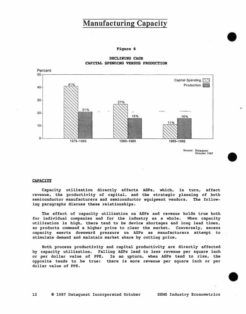
An important implication of rising capital productivity is that as capital becomes more productive, it will take less equipment to generate any given amount of revenue. Figure 6 illustrates the effects of increasing capital productivity on the growth rate of capital spending. Historically, the growth rate of capital spending has been greater than that of semiconductor production. We believe that the reverse will be true in the future. This is particularly important to equipment manufacturers. Upsurges in capital spending will no longer lift equipment vendors as high as they have in the past. There will still be growth, but not as strong as in previous years.
Demand for materials, too, will be weakened by the improvement of capital productivity. As line balance and utilization improve through the increased use of computer-aided manufacturing, there will be a corresponding decrease in work-in-process (WIP) inventory. This effectively shortens cycle times and thus lowers the probability of particulate contamination. As yields tend to increase, there will be less of an increase in materials usage for any given increase in semiconductor revenue. In other words, materials vendors, like equipment vendors, will participate to a lesser degree in semiconductor industry upturns than they have in the past. However, the value added to the devices (usually perceived as quality), and hence the dollar value, will continue to command a significant percentage of the cost of manufacturing.
SEMS Industry Econometrics © 1987 Dataquest Incorporated October 11
Manufacturing Capacity
Figure 6
Percent 5 0 T
DECLINING CA6K CAPITAL SPENDING VERSUS PRODUCTION
40
30
20
10-
4 1 % | . \VV\
27%
Capital Spending [ X M
Production
16%
1975-1985 1980-1985 1985-1992
Source: Dataquest October 1987
CAPACITY
Capacity utilization directly affects ASPs, which, in turn, affect revenue, the productivity of capital, and the strategic planning of both semiconductor manufacturers and semiconductor equipment vendors. The following paragraphs discuss these relationships.
The effect of capacity utilization on ASPs and revenue holds true both for individual companies and for the industry as a whole. When capacity utilization is high, there tend to be device shortages and long lead times, so products command a higher price to clear the market. Conversely, excess capacity exerts downward pressure on ASPs as manufacturers attempt to stimulate demand and maintain market share by cutting price.
Both process productivity and capital productivity are directly affected by capacity utilization. Falling ASPs lead to less revenue per square inch or per dollar value of PPE. In an upturn, when ASPs tend to rise, the opposite tends to be true: there is more revenue per square inch or per dollar value of PPE.
12 © 1987 Dataquest Incorporated October SEMS Industry Econometrics

Manufacturing Capacity
Industry capacity is important to the individual manufacturer in strategic planning for long-term production cycles. When the firm is operating at or near capacity, most of its resources are dedicated to manufacturing existing products rather than developing new products. When industry capacity utilization is high, many firms just cannot fill the demand for their products. Planning for capacity at peaks of industry demand is therefore an excellent strategy to increase market share. Lack of such planning is an equally excellent way to lose market share.
In a downturn, when there is excess capacity, the emphasis is no longer primarily on manufacturing or just getting the product out the door. This is the time for refining manufacturing practices to increase yields and productivity.
Downturns are also the time for the introduction of new products. In a downturn, it is much easier to shift engineers from sustaining-engineering projects to new-product projects. Maskmakers are a good example of this. Reprint work generally correlates with expansions, and new tooling generally coincides with downturns and excess capacity. Basically, new products can stimulate demand and take advantage of unused capacity, without price and margin reductions.
Semiconductor capacity utilization is important not only to semiconductor manufacturers, but also to equipment vendors. North American semiconductor manufacturers generally adjust their capital spending during a downturn in one way—they cut back their capital expenditures when utilization plummets. Knowledge of future utilization would allow equipment vendors to plan their expansions so that their capacity coincides with demand.
When capacity utilization is high, times are good. When capacity utilization is down, times are bad. Accurate forecasting of capacity utilization implies an accurate forecast of the business cycle. Capacity planning will moderate the effects that the business cycle has on individual companies. For the industry as a whole, capacity planning could moderate the business cycle itself. Individual companies engage in capacity planning when they reserve a part of their capacity for a particular large customer. This tends to eliminate double and triple orders, which makes for a more stable and realistic backlog, thereby moderating plans for expansion.
Foundry relationships are another capacity planning method that is growing in popularity, in which both individual companies and the industry as a whole is engaging in capacity management. By using foundry manufacturers for peak demand, major manufacturers are able to shift excess capacity risk to the foundries themselves.
SEMS Industry Econometrics © 1987 Dataquest Incorporated October 13

Manufacturing Capacity
Definition of Capacity
Dataquest measures capacity in square inches of silicon. We have chosen square inches of silicon as our basic measuring unit for the following reasons:
• Silicon is the raw material used and processed in wafer fabrication plants.
• Square inches of silicon is easily measurable.
• Good die per square inch is a good indicator of yield.
• Square inches of silicon is a mojre basic measuring unit than wafer starts/ which aggregates variable-sized wafers.
Capacity is a measure of the ability to produce silicon wafers. It is the amount of silicon in square inches that a semiconductor manufacturer can produce. The sum of all the individual manufacturers' capacity is the capacity of the industry.
Capacity is the maximum output that can be obtained from all the PPE in any given time period. Dataquest has found that on the average over the last 15 years, equipment productivity has tended to be around 80 percent of the maximum; therefore:
Capacity = (Pt(E)/0.8) x PPE
where:
Pt(E) = (trend of square inches of silicon)/PPE.
Capacity Utilization
Dataquest has tracked maximum capacity (as defined earlier in this section) and actual square inches of silicon consumed since 1973. Using Dataquest's estimates of future revenue, future silicon consumption, and future capital expenditures, we have been able to forecast both capacity and capacity utilization. Figure 7 shows the growth of silicon consumption and capacity from 1973 through 1992. Figure 8 shows worldwide capacity utilization, historic and forecast.
Capacity utilization reached an all-time low in 1985 and is now increasing toward another peak in 1988. It will decline slightly in 1989, then climb again to near-record heights in 1991.
14 © 1987 Dataquest Incorporated October SEMS Industry Econometrics

Manufacturing Capacity
F i g u r e 7
WORLDWIDE SEMICONDUCTOR MANUFACTURING CAPACITY ( B i l l i o n s o f Square I n c h e s )
Billions of Square Inciies
3.0
2.7 -
2.4 -
2.1 -
1.8 -
1.5 -
1.2 -
0.9 -
0.6 -
0.3 -
ol
• Consumption
• Capacity
1 — ) 1 1 1 1
> . ^ ^
1 \ T [
1973 1975 1977 1979 1981 19S3 1985 1967 1989 1991
Percent 100
1973
Source: Dataquest October 1987
F i g u r e 8
WORLDWIDE CAPACITY UTILIZATION
1975 1977 1979 1981 1963 1985 1987 1989 1991
Source: Dataquest October 1987
SEMS Industry Econometrics 1987 Dataguest Incorporated October 15


January 13, 1986
SEMICONDUCTOR EQUIPMENT AND MATERIALS SERVICE FILING INSTRUCTIONS
Location: Markets and Technology Binder
Subject: Gases
Pages: 52
Author: Peggy Wood
Filing Instructions: File this service section, dated December 30, 1985, in the Markets and Technology binder behind the Wafer Fabrication Materials tab.

Gases
SOMMARY
In 1984, the gas companies that supply the electronics industry had direct sales of bulk and specialty gases of $205 million to semiconductor manufacturers in the United States. Bulk atmospheric gases (nitrogen, oxygen, hydrogen, and argon) represented $155 million (75.6 percent) of that market. Air Products is the leading supplier of bulk gases in the United States with sales of $72 million (46.4 percent), while the Linde division of Union Carbide is the second largest supplier with sales of $42 million (27.1 percent). Airco and Liquid Air are two other primary bulk gas suppliers to the semiconductor industry and have sales of $21 million (13.6 percent) and $17 million (11.0 percent), respectively.
Nitrogen represented ^ approximately 95 percent by volume or 49.5 billion cubic feet (Bcf) of the bufk atmospheric gases sold in the United States in 1984. Hydrogen and oxygen each represented an additional 2 percent by volume, while argon was approximately 1 percent by volume of the total bulk gas consumption by the U.S. semiconductor industry in 1984.
The nitrogen gas market in 1984 represented a substantial portion of the bulk gas supplied to the semiconductor industry in the United States, in both sales ($118.8 million) and volume (49.5 Bcf). The consumption of nitrogen is dependent not only on wafer starts but also on the installed base of equipment in fabrication facilities. Nitrogen flow is used to maintain the integrity of many pieces of processing equipment during times of nonproduction, and thus the nitrogen market exhibits surprising stability during the economic downturns in the semiconductor industry.
Specialty gas sales to semiconductor manufacturers in the United States represented the remaining $50 million (24.4 percent) of the $205 million gas market in 1984. Pour major suppliers of specialty gases (in order of market share) include Airco, Linde, Air Products, and Matheson, with market shares ranging from 21 percent to 15 percent. Suppliers with smaller shares include Scientific Gas Products, Liquid Carbonic, and Liquid Air.
The total worldwide market for bulk and specialty gases supplied to the ^semiconductor industry in 1984 was $430.5 million. As mentioned above, the U.S. market represented $205 million in sales, or 47.6 percent of the world market. In Japan, bulk and specialty gas sales totaled $157 million (36.5 percent), while the gas market in Europe in 1984 was $32 million (7.4 percent). In Rest of World (ROW), the sales of bulk and specialty gases to the semiconductor industry were $36.5 million (8.5 percent). The ROW gas market may seem surprisingly large for the level of semiconductor production in those areas. However, there is a large nitrogen requirement for assembly operations of devices manufactured in the United States and Europe.
SEMS Markets and Technology © 1985 Dataquest Incorporated Dec. 30 ed.

Gases
OVERVIEW
In the semiconductor industry, process gases represent one category of consumable materials that are used throughout the fabrication of semiconductor devices, from the growing of single silicon crystals, through the many steps of wafer fabrication, to the final stages of assembly and packaging. Gases are divided into two general categories; bulk atmospheric gases and specialty gases.
Bulk atmospheric gases (BAG) include nitrogen, oxygen, hydrogen, and argon. Hydrogen is available in only trace amounts in the atmosphere and thus it is generated through hydrocarbon refining rather than through air separation. However, because it is typically supplied in bulk amounts to semiconductor manufacturers, it is included under—the bulk—atmospheric gases designation. The designation "bulk" refers specifically to a discrete delivery of gas in its liquid state. These gases typically are delivered as cryogenic liquids because of the efficiency of transportation and storage prior to the vaporization stage from the liquid to a gas at the semiconductor fabrication facility. For the purpose of this study, nitrogen gas provided through direct pipeline delivery, as well as customer on-site nitrogen generation plants, are also considered under the-^ulk atmospheric gases category even though the supply of nitrogen, in this sense, cannot be classified as discrete.
There are a large number of gases (more than 35} that can be classified as specialty gases. For that reason, a further segmentation of this category is necessary, and is based on the chemical reactivity and functionality of the various specialty gases. For the purposes of this study, the specialty gas segmentation is defined as follows:
(ft Silicon-precursor gases (i.e., silane, dichlorosilane, trichlorosilane, and silicon tetrachloride),
• Dopants (i.e., arsine, phosphine, and diborane)
ii Plasma etchants (i.e., carbon tetrafluoride, as well as numerous other halocarbon and fluorine-based gases)
• Reactant gases (i.e., ammonia, hydrogen chloride, nitrous oxide, and carbon dioxide)
• Atmospheric/purge cylinder gases (i.e., nitrogen, hydrogen, oxygen, argon, and helium)
• Others (i.e., tungsten hexafluoride and germane)
& 1985 Oataquest Incorporated Dec. 30 ed. SEMS Markets and Technology

Gases
Specialty gases are used in comparatively smaller volumes than the bulk atmospheric gases and thus are delivered to a semiconductor manufacturer in high-pressure cylinders. Note that nitrogen and other atmospheric gases appear in one of the specialty gas categories as well as under the bulk gas designation. The distinction in this case is that these gases are supplied in gas cylinders rather than in discrete deliveries of bulk liquid. These gases are used primarily for purging certain processing systems and equipment in cases when a semiconductor manufacturer is concerned about possible back-contamination of the house lines of nitrogen, hydrogen, argon, etc.
The following section will review the various bulk and specialty gas categories and summarize their applications in the semiconductor manufacturing process. Table- 1 contains a compr-«hensive—list of the gases that are used in semiconductor manufacturing.
I.
Table 1
BULK AND SPECIALTY GASES USED IN SEMICONDUCTOR MANUFACTURING
BULK ATMOSPHERIC GASES
Nitrogen, N2 Oxygen, O2
Hydrogen, H2 Argon, Ar
II. SPECIALTY GASES
A. Silicon-Precursor Gases
Silane, SiH4 Trichlorosilane, SiHCl3
B. Dopants
Arsine, ASH3 Phosphine, PH3 Diborane, B2H5
Dichlorosilane, SiH2Cl2 Silicon Tetrachloride, SiCl4
Boron Trichloride, BCI3 Boron Trifluoride, BF3 Phosphorous Pentafluoride, PF5
^Continued)
SEMS Markets and Technology © 1985 Dataquest Incorporated Dec. 30 ed. 3

Gases
Table 1 (Continued)
BULK AND SPECIALTY GASES USED IN SEMICONDUCTOR MANUFACTURING
II. SPECIALTY GASES (Continued)
C. Plasma Etchants
Carbon Tetrafluoride, CF4 Fluoroform, CHF3 Hexafluoroethane, C2F5 Dichlorodifluoromethane, CCI2F2 Bromotrifluorometiiane, CBrF3 Chlorotrifluoromethane, CCIF3 Chloropentafluoroethane, C2CIF5 Methyl Fluoride, CH3F Trichlorofluoromethane, CCI3F Perfluoropropane, C3Fg Chlorine, CI2 Carbon Tetrachloride, CCI4 Silicon Tetrafluoride, SiF4 Sulphur Hexafluoride, SFg Nitrogen Trifluoride, NF3 Others
(Halocarbon-14) (Halocarbon-23) (Halocarbon-116) (Halocarbon-12) (HalDcarbon=13Bl) (Halocarbon-13) (Halocarbon-115) (Halocarbon-41) (Halocarbon-11)
D. Reactant Gases
Ammonia, NH3 Hydrogen Chloride, HCl
Nitrous Oxide, N2O Carbon Dioxide, CO2
E. Atmospheric/Purge Cylinder Gases
Nitrogen, N2 Hydrogen, H2 Helium, He
Oxygen, O2 Argon, Ar
F. Others
Tungsten Hexafluoride, WFg Germane, GeH4 Others
Source: DATAQUEST
© 1985 Dataquest Incorporated Dec. 30 ed. SEMS Markets and Technology

Gases
APPLICATIONS—BULK ATMOSPHERIC GASES
Nitrogen
Nitrogen is the most widely used gas in the semiconductor industry, in both wafer fabrication as well as assembly operations. Its consumption by volume represents approximately 95 percent of all bulk atmospheric gases used in semiconductor manufacturing. Its primary application is in providing an inert atmosphere for the various wafer processing systems such as epitaxial reactors, chemical vapor deposition (CVD) reactors, and diffusion furnaces. Nitrogen is used as a transportation medium in some wafer processing equipment. In addition, it is used as an inert .^environment djiring the .£xposure__Qf_ negative photoresist in lithography because of the necessity to minimize competitive oxygen side reactions that can lead to film thickness losses. Nitrogen is also used to maintain the integrity of various pieces of processing equipment, such as furnace banks, even while they are not in direct production use. In some facilities, certain clean stations are equipped with constant flows of nitrogen to maintain ultraclean conditions. Many other pieces of equipment in a fab use nitrogen, including blow guns, pneumatic-actuated valves, spin rinse dryers, dessicators, and cryo pumps used for condensing contaminants in vacuum systems. Because of the emphasis on the use of high-purity materials in the semiconductor industry, nitrogen purity is typically "five nines" (99.999 percent) to "six nines" purity.
Oxygen
Oxygen has the capability to form oxides with all elements except inert gases. In wafer fabrication, it is used to form dielectric and passivation layers of silicon dioxide (Si02) on silicon substrates (MOS devices, in particular). It is also used as a component in certain halocarbon plasma etch mixtures such as carbon tetrafluoride (CF4) and oxygen for the etching of silicon dioxide and silicon nitride layers. Its usage represents only a few percent by volume of the bulk atmospheric gases consumed by the semiconductor industry.
Hydrogen
Hydrogen is most commonly used as an ambient environment for the growth of epitaxial layers. It is also used as a carrier gas during diffusion processes to provide a reducing environment in such reactions as the conversion of boron trichloride to atomic boron.
SEMS Markets and Technology © 1985 Dataquest Incorporated Dec. 30 ed. 5

Gases
Hydrogen is used with oxygen in oxidation processes to form water vapor at oxidation temperatures in what is called a wet-ox (wet oxidation) process. Typically, silicon and oxygen react directly to form silicon dioxide, but the formation of thicker oxide layers requires prohibitive amounts of production time. When silicon reacts with water vapor to produce silicon dioxide and hydrogen, the oxide layer forms at an increased rate due to the relatively fast diffusion of a hydroxyl species. Hydrogen that has been included in the silicon dioxide film is driven off by subsequent heating steps such as diffusion, and densification of the oxide occurs.
Hydrogen consumption, like that of oxygen, represents only a few percent by volume of the bulk atmospheric gases used in the semiconductor industry. ^ - _ ^^.^
Argon
Argon is used by the semiconductor industry primarily as an inert environment for the growth of single-crystal silicon, and also has applications in sputtering and ion implantation. There is currently a trend toward increased usage of argon in the annealing process for thin gate oxides because of the truly "inert" nonreactive nature of the gas. Argon costs more than nitrogen, which has been the traditional choice for an inert environment in this process. However, the extra expense at such a late stage of fabrication is considered minimal compared with potential device failure, and hence lower yields, caused by chemical contamination during the annealing process.
Argon consumption represents approximately one percent of the total volume of bulk atmospheric gases consumed by the semiconductor industry, and consumption is split between usage in single silicon crystal growth and fabrication processing.
SPECIALTY GASES
Silicon-Precursor Gases
The silicon-precursor gases such as silane, dichlorosilane, trichlorosilane, and silicon tetrachloride are used in epitaxial and chemical vapor deposition (CVD) processes to deposit layers of silicon or silicon compounds (i.e., silicon dioxide, silicon nitride) onto silicon substrates. Silane, in particular, is used in PECVD (plasma-enhanced CVD) for the deposition of amorphous and polysilicon layers. Dichlorosilane is also a primary source for the deposition of polysilicon.
6 © 1985 Dataquest Incorporated Dec. 30 ed. SEMS Markets and Technology

Gases
Silicon epitaxial layers are formed in reactions based on mechanisms of thermal decomposition or reduction by hydrogen, depending on the silicon-precursor reactant gas. Each of the silicon-precursor gases has epitaxial processing advantages and disadvantages, which include the processing temperature range, degree of autodoping, and growth rates. Silane is a pure gaseous source, while silicon trichloride and silicon tetrachloride are both corrosive liquids at room temperature and pressure. Oichlorosilane is in a gaseous state at a pressure of 0.5 atmospheres. The typical epitaxial reactions, temperature ranges, growth rates, and processing advantages and disadvantages are summarized in Table 2.
Table 2
EPITAXIAL SOURCES: ADVANTAGES AND DISADVANTAGES
Reactions
Thermal Decomposition
SiH4 •Si + 2H2 SiHoCl- -•Si + 2HC1
Reduction by Hydrogen
Temperature Range
1,000 to 1,050° C 1,050 to 1,100° C
Temperature Range
Growth Rate
0.2 to 1.0 M/min ^1.0 M/min
Growth Rate
SiHCl3 + H2 SiCl4 + 2H2
Source
•Si + 3HC1 ^•Si + 4HC1
Advantages
1,150 to 1,200° C 1,150 to 1,200° C
1.0 to 10 At/min 0.5 to 1.5 M/min
Disadvantages
SiH/ Low-temperature deposition Low autodoping
Pyrophoric gas Moderate growth rates
SiCl/ Moderate to high growth rates Easy to obtain good crystal quality on thick layers
Corrosive liquid High-temperature deposition Moderate autodoping
SiHCl3 Very high growth rates Very high purity epitaxial layers
Most common source of poly-Si
Corrosive liquid High-temperature deposition Moderate autodoping
SiH2Cl2 Properties intermediate between SiH4 and SiCl4
Source: DATAQUEST
SEMS Markets and Technology © 1985 Dataquest Incorporated Dec. 30 ed.

Gases
A layer of silicon dioxide is formed when silane and oxygen react together in an oxidation process. The other silicon-precursor gases form oxide layers when they undergo hydrolysis (reaction with water) in a moist atmosphere.
Oxidation Sifl4 + O2 • S i 0 2 + 2H2
Hydrolysis SiH2Cl2 + 2H2O »-Si02 + 2HC1 + 2H2 SiHCl3 + 2H2O •Si02 + 3HC1 + H2 SiCl4 + 2H2O •Si02 + 4HC1
Silane and dichlorosilane both react with ammonia to form passivation layers of silicon nitride.
3SiH4 + 4NH3 •Si3N4 + I2H2 3SiH2Cl2 + 4NH3 •Si3N4 + 6HC1 + 6H2
As mentioned previously, each of the silicon-precursor gases has processing advantages and disadvantages. The safety issue is particularly important with regard to silane as it is a pyrophoric gas, which means that_it will burn upon exposure to air. Silicon tetrachloride (siltet) on the other hand, while corrosive, is not classified as toxic nor does it ignite in air. However, it does require the highest operating temperature of all the silicon-precursor gases for epitaxial deposition (1,200° C). In addition, unlike silane, siltet can cause pattern shifts in epitaxial layers due to the formation of chlorine radicals.
The chemical characteristics of dichlorosilane and trichlorosilane fall between those of silane and silicon tetrachloride. Both operate in an intermediate temperature range between silane and siltet. While toxic and corrosive, neither one is considered pyrophoric. In addition, both can cause some degree of pattern shift in epitaxial deposition.
Dopants
Dopants are used as a source of controllable impurities within semiconductor devices. A known concentration and type of impurity (n or p) is introduced into specific regions to modify local electrical properties of the medium. Specifically, an element contributes either an excess hole (p dopant) or electron (n dopant) to the local structure of the crystal lattice, which in turn alters the conductivity of the material. For silicon, the p and n dopants are found in Groups III and V, respectively, of the periodic table. Dopants are available in liquid, solid, and gaseous states. The common gaseous n dopants are arsine and
8 e 1985 Dataquest Incorporated Dec. 30 ed. SGMS Markets and Technology

Gases
phosphine, while the common gaseous p dopants include diborane and boron trichloride. Boron trichloride is also used in plasma etching, as well as in chemical vapor deposition of BPSG (borophosphosilicate glass). Dopants are utilized in epitaxial deposition, diffusion, and ion implantation.
In diffusion processes, the dopant gas, which is frequently mixed with nitrogen or hydrogen, is introduced into a high-temperature oven (950-1,280° C) and is incorporated into the substrate by a diffusional mechanism. A dopant concentration gradient in the substrate material is established and the depth of diffusion is controlled by process time and temperature.
The common carrier gases for dopants in diffusion processes are nitrogen and hydrogen, as rSentioned previrously, although argon and helium are also used. Arsine and phosphine may be supplied to a semiconductor manufacturer as pure gases or as premixed dilutions with these atmospheric gases. Arsine and phosphine premixed with silane are also available. As diborane is extremely unstable in its pure form, and decomposes at a rate of 0.5 percent per day at room temperature, it is always supplied to semiconductor manufacturers diluted with other gases; typically, 15 percent diborane in nitrogen, hydrogen, argon, or helium.
Arsine, phosphine, and diborane gases are all highly poisonous materials. Arsine has a disagreeable garlic-like odor, and inhalation of as little as 0.5 parts per million is considered to be dangerous. Phosphine has an unpleasant odor of decaying fish and will react violently in the presence of an oxygen environment. Diborane is described as having a repulsive, sickly sweet odor, and is spontaneously flammable in air above a temperature of 40° C. However, in the presence of certain contaminants, the ignition of diborane/air mixtures may occur at or even below room temperature. For these reasons and other safety issues, primary manufacturing of these gases is limited to only a handful of companies.
Ion implantation, and more recently neutron transmutation, offer a substantial amount of processing control over diffusion. In ion implantation, the dopant atoms are ionized and accelerated to high energies. The ion beam is directed and focused onto the wafer and the high-energy ions penetrate the surface. Ion implantation offers a great deal of process control because ion current and implant time can both be measured, and thus the number (dosage) of dopant ions incorporated into the material as well as the concentration profile can be determined. In ion implantation, room temperature processing minimizes dopant migration in the substrate, particularly beneath critical gate structures. Because the dopant profile can be controlled/ smaller line geometries can be
SEMS Markets and Technology © 1985 Dataquest Incorporated Dec. 30 ed.

Gases
achieved. In addition to arsine and phosphine, boron trifluoride and phosphorous pentafluoride are also used as dopant source gases in ion implantation.
One disadvantage to ion implantation compared with diffusion is that as the dopant ions collide with the wafer, a significant amount of damage can occur to the crystal lattice. Most of this damage, however, can be later repaired in subsequent annealing steps.
There is an increasing trend away from diffusion and toward ion implantation as a doping procedure for the small-geometry devices because of the greater degree of process control. This trend will have some impact on the gas industry since the diffusion process consumes large amounts of nitrogen in addition to the dopant soure«-gases.—However, it is unlikely that diffusion will completely disappear in the future, but rather, will likely remain a standard technique for introducing dopant materials in the larger-geometry devices.
Neutron transmutation doping (NTD) is a new technique for n-type doping that primarily has been limited to high-power applications. In this process, silicon wafers are placed in a nuclear reactor and a stream of thermal neutrons is passed through them. Some of the silicon atoms in the lattice are altered to phosphorous through a nuclear mechanism. While the technique can only form phosphorous-doped materials, it has its advantages in that it can provide an extremely uniform distribution of phosphorous in silicon. In addition, no. external source of dopant material is required, as the silicon provides its own. One disadvantage, however, is that access to a nuclear reactor is required. Currently this technique is still quite limited in its applications and production capability. However, it may prove to be a viable alternative for doping semiconductor devices at some future time.
Plasma Etchants
A wide variety of gases, primarily halocarbons, are used in plasma etching. The choice of gases is strongly dependent on the ability of a given mixture of gases to selectively etch one film in the presence of another with a sufficient degree of profile control. The advantages of plasma etch over wet etching techniques include the ability to generate anistropic (i.e., sharp-walled) as well as isotropic (curved-walled) profiles. In addition, loss of photoresist adhesion is minimized in plasma compared with wet etch. Also, because the etching materials are gases, smaller quantities of reagents are used and thus smaller amounts of waste chemicals are generated.
10 © 1985 Dataquest Incorporated Dec. 30 ed. SEMS Markets and Technology

Gases
From a conceptual point of view, plasma etch is a fairly simple process. A highly reactive gaseous species is generated that reacts with the wafer surface to produce a volatile etch product. For most semiconductor materials and metals, the plasma is used as a source of halogen atoms to generate volatile halide etch products. The etching of organic films is best achieved when the plasma provides a source of oxygen atoms to form volatile products such as carbon monoxide (CO).
It is difficult to establish a quantitative relationship to describe the consumption of halocarbon gases in the plasma etch process, since the physical and chemical mechanisms that determine plasma etch efficiency are still not fully understood. For that reason, plasma etch has been described as more of an art than a science, and most process engineers exercise a great deal of fjreedpm in establishing their own unique plasma etch gas mixtures.
Carbon tetrafluoride (CF4) is probably the most commonly used plasma etch gas. It is an odorless, colorless gas that is stable and nontoxic. It is capable of etching silicon in both its pure gaseous form and when mixed with oxygen. It is also known as tetrafluoromethane, halocarbon-14, or Freon-14. (Freon is a registered trademark of Dupont.) Fluoroform (CHF3, trifluoromethane, halocarbon-23) and hexafluoroethane (C2F5, halocarbon-116) are also used in large quantities. Please refer to Table 1 for a more comprehensive list of plasma etchants. The following sections give examples of the gases that are used to etch silicon and polysilicon, silicon dioxide and nitride, silicides, metals, and photoresist.
Etching of Silicon and Polysilicon
For any given plasma etch mixture, it is very important to be able to selectively etch one film in the presence of another. Selectivity for isotropic etching of silicon and polysilicon in the presence of oxide is very high when using the fluorine-source plasmas (such as CF4/O2, SiF^, SFg, and NF3). Typically, anistropic profiles are difficult to achieve when using fluorine sources; however, a high degree of anistropy can be obtained with plasmas that produce chlorine and bromine atoms (CI2, CI2 C2F6, CF3CI C2Fg, Br2, and CF3Br).
It is believed that the underlying mechanism for achieving such anistropic profiles may be the physical ion bombardment of the surface. Isotropic profiles are easier to obtain when etching silicon and polysilicon with fluorine sources, and are believed to be due to chemical etching by fluorine atoms.
SEMS Markets and Technology © 1985 Oataquest Incorporated Dec. 30 ed. 11

Gases
Etching of Silicon Dioxide and Nitride
The plasma gases that are used to etch silicon dioxide and nitride in the presence of silicon include CP4/H2f CHF3, and C2F6. It has been established empirically that high degrees of selectivity for etching oxide and nitride layers are achieved by the addition of fluorine scavengers such as methane, ethylene, and hydrogen, thereby establishing a fluorine-deficient chemical environment. The underlying chemistry is not clearly understood, and the fine-tuning of feed gases to the plasma discharge is still empirical in nature.
Etching of Silicides
Silicides of titanium (Ti), tantalum (Ta), molybdenum (Mo), and tungsten (W) are commonly etched with a mixture of CF4 and O2. Highly volatile silicon tetrafluoride (SiF4) is produced, as well as moderately volatile metal fluorides. Isotropic as well as anistropic profiles have been reported. We expect this area of plasma etch to continue to receive attention with the increasing trend toward CVD-tungsten silicide applications in MOS devices.
Etching of Metals
In etching metal layers, it is critical that water vapor and oxygen be excluded from the plasma reactor (or possibly scavenged) because of the formation of native metal oxides at the surface. Chlorocarbon and fluorocarbon gases are typically used to etch metal films rather than pure halogens, because of their ability to reduce the native oxides chemically. Nitrogen trifluoride (NF3) is helpful in increasing selectivity over silicon dioxide films.
Aluminum and chromium do not form volatile metal fluorides, and therefore, etching of these metals is best carried out in plasmas that generate chlorine atoms. Gases that efficiently scavenge oxygen and moisture include boron trichloride (BCI3) and silicon tetrachloride (SiCl4). In addition, they form radicals that react with the native oxide. Once the native oxide has been removed, aluminum may be etched spontaneously in a pure chlorine environment. Both anistropic and isotropic etches can be achieved depending upon the amount of molecular chlorine in the plasma mixture.
Etching of Photoresist
Photoresist and organic films are often stripped by plasma systems that generate atomic oxygen. Rare gases and CF4 are added to stabilize the discharge and enhance the reactivity of the organic material. The
12 © 1985 Dataquest Incorporated Dec. 30 ed. SEMS Markets and Technology

Gases
discharge produces such etch products as carbon monoxide, carbon dioxide, and water. If the plasma is rich in atomic oxygen, high selectivities over silicon dioxide, silicon nitride, and metals can be achieved.
Reactant Gases
Reactant gases include ammonia, hydrogen chloride, nitrous oxide, and carbon dioxide. Ammonia is typically used with either silane or dichlo-rosilane to produce silicon nitride layers in chemical vapor deposition. Silicon nitride films are used as passivation layers or interlayer dielectrics in semiconductor devices. Ammonia is a corrosive, alkaline gas that is considered toxic. It is generally regarded as nonflammable, and has a distinctive pungent odor.
Hydrogen chloride is used to polish and etch wafers prior to deposition steps by removing defects on the wafer surface due to mechanical polishing and handling of the wafer. A significant development in thermal oxidation has been the use of hydrogen chloride in combination with oxygen. Hydrogen chloride is particularly effective in gettering mobile sodium ions and other impurities in the wafer, which in turn helps minimize leakage in the MOS gate threshold voltage. Hydrogen chloride is a colorless, corrosive, nonflammable, acidic gas that has a repulsive odor. Because of its corrosive nature, special attention must be focused to maintain the purity of the gas. In particular, contamination can result from the interaction between hydrogen chloride and the walls of gas cylinders.
Nitrous oxide and carbon dioxide are both used as sources of oxygen in silicon oxide films formed in chemical vapor deposition processes. Nitrous oxide is available as a liquefied gas. It has a sweet odor and is generally used as an anesthetic. It is commonly known as "laughing gas." However, nitrous oxide becomes a strong oxidizing agent at temperatures greater than 300° C. Carbon dioxide is a colorless, odorless, noncombustible gas.
Atmospheric/Purge Cylinder Gases
As mentioned previously, nitrogen and other atmospheric gases are also supplied to semiconductor manufacturers in cylinders as well as in discrete deliveries of bulk liquids. They are classified under the specialty gas designation because they represent cylinder deliveries. These gases are used primarily for purging certain processing systems and equipment in cases when a semiconductor manufacturer is concerned about possible back-contamination of the house lines. In addition, there are
SEMS Markets and Technology e 1985 Oataquest Incorporated Dec. 30 ed. 13

Gases
some processes, such as sputtering, that require small amounts of gas, and thus single-cylinder usage is more economical. In the case of sputtering, the process is run under vacuum conditions and argon ions are accelerated in an electric field. Through physical bombardment, the argon ions knock molecules off the surface of a solid target. The ejected material from the target is deposited onto the surface of a wafer, in addition to the walls of the sputtering chamber. Typically, a cylinder of argon can last for three months or more in a sputtering system before it requires replacement.
Other Specialty Gases
In this specialty gas_^category can be found such gases__as_ tungsten hexafluoride and germane. Germane, GeH4, is used in epitaxial chemical vapor deposition for the manufacturing of LEDs. Germane must be used with great caution as it is a hemolytic gas, and thus has the ability to dissolve red blood cells.
Tungsten hexafluoride, WFg, is used as a source of tungsten for the deposition of tungsten silicide as an alternative interconnect material in VLSI devices. The deposition of refractory metal silicides is an area that is receiving increased attention as semiconductor manufacturers design IC devices with higher packing densities and higher device speeds. The problem is that while scaling improves overall device performance, a reduction in device geometries also results in a corresponding reduction of the thickness of interconnect lines. In addition, the larger die sizes used in VLSI devices typically require longer interconnect lines. This combination of thinner and longer interconnect lines results in an increase in the interconnect, resistivity and hence, in the RC time delay of the circuit.
Tungsten silicide, as well as other refractory metal silicides based on molybdenum, tantalum, and titanium, have been developed as interconnect materials for VLSI devices because they exhibit considerably reduced resistivities. When these refractory metal silicides are deposited at the gate level on a layer of doped polysilicon, the resulting structure is called a "polycide" shunt. The polycide structure has the advantage of the reduced resistivity of the refractory metal silicide and yet retains the good performance characteristics of polysilicon, such as the stable polysilicon/oxide interface.
The techniques of deposition of refractory metal silicides include sputtering, coevaporation, and chemical vapor deposition. The source materials for molybdenum, titanium, and tungsten are molybdenum hexafluoride, titanium tetrachloride, and tungsten hexafluoride, respectively.
14 © 1985 Dataquest Incorporated Dec. 30 ed. SEMS Markets and Technology

Gases
These materials are all liquids at 25° C that have sufficient vapor pressure to allow for source flow to be controlled with a mass flow controller. Tungsten hexafluoride, in particular, is a yellow liquid at room temperature. In its gaseous state, it forms a white mist of hydrogen fluorine gas in moist air. In an inert environment, tungsten hexafluoride is a colorless, odorless gas.
DATAQUEST believes that tungsten silicide is the most widely used refractory metal silicide in the United States. Genus, a CVD manufacturer, was the first to develop a dedicated tungsten silicide reactor for liquid phase chemical vapor deposition, and the success of the Genus reactor has done much to stimulate interest in tungsten hexafluoride as a source material.
SUMMARY OF PHYSICAL CONVERSION FACTORS
Gas, by its very nature, is available in a variety of different volumes and quantities depending on the temperature and pressure of the system. The associated nomenclature used to describe a given amount of gas is likewise as varied. The following section presents a summary of the different units of temperature, pressure, volume, and weight that are commonly used in the gas industry, as well as a set of conversion factors between the different units.
Any amount or quantity of gas has a temperature and pressure dependence that in its simplest form is governed by the Ideal Gas Law, PV = nRT. This law states that the pressure of any gas, P (measured in atmospheres), multiplied by its volume, V (liters), is equal to the product of the number of moles of the gas, n, multiplied by the temperature of the system, T (in kelvins) , and the universal gas constant, R. One convenient way to remember the appropriate factors is that one mole of gas at one atmosphere pressure at 0° C (273 K) will occupy 22.4 liters.
STP is the designation that is used to indicate standard temperature and pressure; by definition, one atmosphere, 0° C (273 K) . The more common specification is that of NTP, which stands for normal temperature and pressure, and corresponds to one atmosphere, 70° F. One atmosphere of pressure can also be defined in units of pounds per square inch; specifically, one atmosphere of pressure is equal to 14.7 psi. An alternative designation is gauge pressure, or psig (pounds per square inch gauge) , which does not include ambient pressure conditions. Finally, psia (pounds per square inch absolute) is the sum of gauge pressure as well as the atmospheric pressure, typically 14.7 psi.
SEMS Markets and Technology © 1985 Dataquest Incorporated Dec. 30 ed. 15

Gases
Common units for volume include liters, cubic feet (cf), and cubic meters (cm, not to be confused with centimeters). In some cases, cubic feet will be specifically identified as standard cubic feet (scf) which defines the temperature and pressure values at NTP. However, while "scf" may not be directly stated, in general it is assumed that NTP conditions hold unless otherwise specified. Large quantities of gas are usually described in units of hundred cubic feet (hcf), billion cubic feet (Bcf), or hundred cubic meters (hem); this last designation is pronounced "hook-ems."
The units of kilograms, pounds, and tons are also used to designate a given quantity of gas under normal temperature and pressure. The definition of a ton, and thus the conversion factor from tons to pounds, takes on a different value in jthe United States compared with Europe and Japan. In the United States, one ton~is equal to 2,000 pounds. In Europe and Japan, the designation of metric tons is assumed, in which case one metric ton is equal to 2,204 pounds (1,000 kg). Table 3 contains a summary of temperature, volume, and weight conversion factors.
Table 3
PHYSICAL CONVERSION FACTORS
Temperature
Fahrenheit (O F) = 1.8 * o C + 32 Celsius (O C) = (5/9) * (° F-32) Kelvin (K) = o C + 273
Volume
1 liter = 1,000 cubic centimeters 1 cubic foot = 28.32 liters 1 cubic meter = 35.31 cubic feet = 1,000 liters 1 hem = 100 cubic meters = 3,531 cubic feet 100 Bcf = 28.32 million hem (million hundred cubic meters)
Weight
1 kg = 2.204 pounds 1 ton = 1,000 pounds 1 metric ton = 1,000 kg = 2,204 pounds
Source: DATAQUEST
16 O 1985 Oataquest Incorporated Dec. 30 ed. SEMS Markets and Technology

Gases
GAS COMPANIES SUPPLYING THE SEMICONDUCTOR INDUSTRY
Table 4 contains a listing of the major bulk and specialty gas companies that directly supply the semiconductor industry in the United States, Japan, and Europe. The companies are listed in alphabetical order rather than by regional market share. The individual companies and their regional trading partners and joint ventures will be discussed in the following sections.
. _ Table 4 _
GAS COMPANIES BY REGION
United States
Air Products Airco Liquid Air Liquid Carbonic Matheson Scientific Gas Products Union Carbide (Linde)
Japan
Oaido Sanso Iwatani Nippon Sanso Osaka Sanso Seitetsu Kagaku Showa Denko Taiyo Sanso Takachiho Teisan
Europe
Air Products B.O.C., Ltd. L'Air Liquide Linde AG Matheson Messer Griesheim Union Carbide (Linde)
Source: DATAQUEST
United States
In the United States, there are essentially only four companies that supply bulk atmospheric gases to the semiconductor industry: Air Products & Chemicals, Airco Industrial Gases, Liquid Air Corporation, and the Linde division of Union Carbide Corporation. While all four companies serve the industrial gas market in addition to the semiconductor industry. Air Products and Union Carbide have a diverse range of business operations beyond gases. Air Products supplies chemicals and
SEMS Markets and Technology © 1985 Dataquest Incorporated Dec. 30 ed. 17

Gases
engineering services in addition to industrial gases and related equipment. In 1984, Air Products acquired a minority interest in UTI Instruments Company, an analytical instrumentation firm, as well as an interest in Benzing Technologies, a plasma processing equipment company that utilizes nitrogen trifluoride gas to clean CVD reactors. To complement its acquisitions in high-technology firms. Air Products has also formed a joint venture with Celltech, Ltd., one of the leading biotechnology companies in Great Britain.
Union Carbide Corporation is a large, multinational corporation with business divisions in chemicals, plastics, and metals as well as its industrial gas operations. In addition. Union Carbide has polysilicon facilities in the United States and owns KTI Chemicals, Inc., a photoresist company that also supplies pellicles tCL the -semiconductor industry. In 1984, Union Carbide purchased Phoenix Research, a primary manufacturer of high-purity arsine, phosphine, and gaseous hydrogen chloride. Phoenix Research is one of only three companies that has primary arsine manufacturing capability. Air Products and Union Carbide rank first and second in sales of total bulk and specialty gases to the semiconductor industry in the United States with a combined market share of more than 60 percent.
Liquid Air is an operating company that is 90 percent-owned by L'Air Liquide, a French gas company that is the largest industrial gas company in the world. Airco is owned by British Oxygen Company, B.O.C., Ltd., which is headquartered in the United Kingdom.
All four companies provide on-site nitrogen facilities as well as bulk liquid deliveries of nitrogen, oxygen, argon, and hydrogen. Both Air Products and Linde have nitrogen pipeline systems, though the two Air Products networks (Silicon Valley and Chandler, Arizona) are much more extensive than the new Linde system (San Jose, California). Air Products and Linde also have liquid hydrogen manufacturing facilities.
The major specialty gas suppliers to the semiconductor industry include Air Products, Airco, and Linde. Liquid Air's new specialty gases division, Alphagaz, is a recent entrant in the market and currently represents a percent or less of sales to the semiconductor industry. Ideal Gas Products is part of the Alphagaz Specialty Gases Division of Liquid Air.
Other specialty gas companies include Liquid Carbonic, Matheson Gas Products, and Scientific Gas Products. Matheson was purchased in 1983 in a joint venture between Amerigas and the Japanese industrial gas company, Nippon Sanso. Matheson's European operations were purchased at the same time by Union Carbide Corporation. Scientific Gas Products is part of the Ashland Chemical Company, a major supplier of wet chemicals and acids to the semiconductor industry. Ashland Chemical Company, in turn, is part of Ashland Oil.
18 © 1985 Dataquest Incorporated Dec. 30 ed. SEMS Markets and Technology

Gases
Europe
The major gas companies that supply the European semiconductor industry include Air Products, B.O.C., L'Air Liquide, Linde AG, Matheson, Messer Griesheim, and Union Carbide.
Union Carbide does not use the Linde name for its gas operations in Europe because the West German gas company, Linde AG, has rights to worldwide use of the Linde name outside of North America. (Dr. Karl von Linde was the German scientist who developed and patented the technique of cryogenic air separation in 1895.) Linde AG, one of the world leaders in air liquefaction plants, has recently started to focus on the electronic gases market. It has a new specialty gas handling facility outside of Munichy^ which is expected to be on-line icj^te 1985.
In addition to its other international facilities. Union Carbide owns the European operations of Matheson (headquartered in Belgium). Union Carbide also has a joint venture with Enichem, a sector of ENI, the Italian state energy group, to market, distribute, and produce industrial and specialty gases in Italy (operational mid-1985). The name of the company is Italiana Gas Industriali S.p.A. (IGI), and it is headquartered in Milan. Union Carbide has plans for a specialty gas manufacturing facility in Scotland; however, final approval for the facility has been postponed for further evaluation in light of the fatal toxic gas leak at the Union Carbide facility in Bhopal, India, in December 1984.
Messer Griesheim is a new entrant in the specialty gas market for the semiconductor industry. It represents a joint venture between Swedish AGA and L'Air Liquide of Prance.
In the United Kingdom, the major gas suppliers are B.O.C. and Air Products. In France, L'Air Liquide has a large majority of the market, with Air Products and Matheson representing the bulk of the remainder. In West Germany, the major gas suppliers include Air Products, Messer Griesheim, L'Air Liquide, Linde AG, and Union Carbide/Matheson. In Belgium, Air Products and Union Carbide/Matheson are the two major suppliers, while in the Netherlands, there are several gas company suppliers to the Phillips semiconductor operations.
Japan
The major gas suppliers to the Japanese semiconductor industry include Daido Sanso, Iwatani, Nippon Sanso, Osaka Sanso, Seitetsu Kagaku, Showa Denko, Taiyo Sanso, Takachiho, and Teisan. The word "sanso" is the Japanese word for oxygen, and thus many of these companies will be listed in the press or in publications as, for example, Daido or Osaka Oxygen.
SEMS Markets and Technology © 1985 Dataquest Incorporated Dec. 30 ed. 19

Gases
Nippon Sanso is the largest oxygen manufacturer in Japan as well as the largest bulk gas supplier to the Japanese semiconductor industry. Nippon Sanso, as well as Showa Denko, a specialty gas supplier to the semiconductor industry, are both part of the Fuyo group. The Puyo group is one of the large industrial entities under which many Japanese businesses are organized, and has as its focus the Fuji Bank. Nippon Sanso, in a joint venture with Amerigas, purchased Matheson Gas Products in 1983. In a second joint venture with Amerigas, Nippon Sanso also acquired an interest in Ansutech, a manufacturer of air separation plants in the United States.
Teisan is a major bulk gas supplier in Japan and is owned by L'Air Liquide of France (major stockholder with 64.2 percent of shares). Teisan currently ranks second -behind Nippon Sanso in-sales of bulk gases to the Japanese semiconductor industry. While Teisan is currently a small player in the specialty gas market, they have plans to promote sales of these gases to the semiconductor and laser industries.
Daido Sanso, a major supplier of oxygen to Japan's steel industry, is experiencing growth in the area of sales of bulk gases to the Japanese semiconductor industry. Air Products is the major stockholder in Daido Sanso with 10 percent ownership of shares. Daido Sanso is part of the Sumitomo group.
Osaka Sanso also supplies bulk atmospheric gases to the Japanese semiconductor industry. B.O.C. of the United Kingdom, through B.O.C. Japan, is the largest stockholder in Osaka Sanso with 23.5 percent of shares. Osaka Sanso is part of the Mitsubishi group.
Taiyo Sanso is a bulk gas supplier to the Japanese semiconductor industry and has Mitsubishi Chemical Industries as its parent company (36.3 percent of shares). Taiyo Sanso is also a member of the Mitsubishi group.
Seitetsu Kagaku is a specialty gas supplier to the Japanese semiconductor industry and is related to Sumitomo Chemical and Nippon Steel through the Sumitomo group.
Takachiho is a specialty gas supplier to the Japanese semiconductor industry and is the trading partner of Synthatron, a New Jersey-based specialty gas manufacturer. Synthatron is a primary manufacturer of arsine, and is a major supplier of dopants to the Japanese market.
Iwatani & Co., Ltd., has formed a joint venture with Union Carbide under the name Iwatani Industrial Gases (IIG) to produce helium, hydrogen, argon, nitrogen, and specialty gases for the Japanese market. The
20 © 1985 Dataquest Incorporated Dec. 30 ed. SEMS Markets and Technology

Gases
facilities are expected to be operational by late 1985, and technology transfer has already been underway for some time. Union Carbide's commitment under the joint venture was more than $10 million, and it will take up to 25 percent in the venture over the next few years. Iwatani & Co. is part of the Sanwa group that has the Sanwa Bank as its focus.
In summary, the major bulk gas suppliers for Japan's semiconductor industry are Nippon Sanso and Teisan with approximately 70 percent of the market. Oaido Sanso, Osaka Sanso, and Taiyo Sanso combined represent an additional 24 percent or so of bulk gas sales. In the specialty gas market, Nippon Sanso and Seitetsu are identified as major suppliers to the semiconductor industry, while Showa Denko, Teisan, and Takachiho maintain a smaller portion of market share. Iwatani did not represent any significant share of the specialty gas market in-JL985.
ROW
The countries with significant semiconductor fabrication under the Rest of World heading include South Korea and Taiwan, while Malaysia, Hong Kong, and Singapore have substantial assembly operations. The major gas suppliers include B.O.C, L'Air Liquide, Nippon Sanso, and Union Carbide either through direct sales or joint venture agreements. Union Gas Co. in Korea is part of the Union Carbide operations, while, for example. Hong Kong Oxygen represents a joint venture between B.O.C. and L'Air Liquide. Because of the large volume of assembly that is conducted in Pacific Rim countries, nitrogen consumption is disproportionately larger than would be expected from nitrogen requirements in semiconductor fabrication operations.
Gas Company Interrelationships
It is clear that while there are half a dozen or more gas companies that supply the semiconductor industry in each of the various regions of the world, there is a large degree of interrelations between the various companies. Two of the major gas companies in the United States, Airco and Liquid Air, are owned by their European counterparts, B.O.C. and L'Air Liquide, respectively. The remaining two major gas companies in the United States, Air Products and Union Carbide, both have major operations established in Western Europe. In Japan, it has been particularly important for the major American and European gas companies to have a Japanese firm as a trading partner or co-joint venturer because of the difficulty of establishing a presence in the Japanese market. Table 5 presents a summary of the regional interrelationships that exist between the major gas suppliers to the worldwide semiconductor industry.
SEMS Markets and Technology © 1985 Oataquest Incorporated Dec. 30 ed. 21

Gases
Table 5
GAS COMPANY INTERRELATIONSHIPS
Japan United States Europe
Overseas Joint Venture Operations
Daido Sanso^^ Air Products ^Air Products
Parent Company Joint Venture of Airco
Osaka Sanso-^ ^ =^ Airco-*-— = -B*jQ»C., Ltd.
t " " ^ I I (Joint Venture) -* '
Same Parent Company Parent Company of Liquid Air
Teisan-* ». Liquid Air.* L'Air Liquide
I (Parent Company of Teisan).* 1
Overseas Joint Venture Operations
Iwatani-* Linde / UCC : ^ Matheson/UCC
Joint Venture Nippon Sanso ^ Matheson
Source: DATAQUEST
BULK ATMOSPHERIC GAS MANUFACTURING
Nitrogen, Oxygen, and Argon
Nitrogen, oxygen, and argon are obtained directly from the air by a technique of cryogenic air separation and distillation. Essentially, the process entails cooling air close to its liquefaction point and then utilizing the physical difference in volatilities of components of air to
22 © 1985 Oataquest Incorporated Dec. 30 ed. SENS Markets and Technology

Gases
distill and separate them. Table 6 contains a list of the fixed components of air by percent composition, as well as the variable components. The fixed components are numbered (in parentheses) in decreasing order of volatility. Those gases in the same volatility range will become impurities of one another. Therefore, helium and neon will sometimes be found in nitrogen, but not in oxygen or argon. Similarly, krypton and xenon will always occur in oxygen, but not in argon or nitrogen. The extent to which any components become impurities in the others is dependent on the separation capacity of the distillation system.
Table 6
COMPONENTS OF THE ATMOSPHERE
Gas
Fixed Nitrogen Oxygen Argon Neon Helium Krypton Xenon
Variable Carbon Dioxide Nitrous Oxide Nitrogen Dioxide Water Hydrogen Carbon Monoxide Methane Ethane Other Hydrocarbons
Order VolatiJ
(3) (5) (4) (2) (1) (6) (7)
of .ity Symbol
N2 02 Ar Ne He Kr Xe
CO2 N2O NO2 H2O
H2 CO CH4
C2H6 C„H„
Concentration-Dry Basis Volume %
78 20 0
1.;
.084
.9476
.934
25*
PPm
18.18 5.24 1.14 0.087
300 to 400 0.5 0 to 0.02
0.5 Typ 1 Typ 2 Typ <0.1 Typ <0.1 Typ
*At 70° F and 50 percent relative humidity
Source: Linde Division Union Carbide Corporation
SEMS Markets and Technology © 1985 Dataquest Incorporated Dec. 30 ed. 23

Gases
#
It is interesting to note that the level of the variable components of the air may differ, depending on the geographical location of a given air separation plant because of the local levels of smog and humidity. Additional purification of the bulk atmospheric gases is necessary in areas that have substandard air quality.
Once the different components of air have been separated, the cryogenic liquids are transported to a customer's site from the gas company's air separation facility in specially equipped tank trucks and tube trailers. Upon arrival at a semiconductor facility, the liquid is transferred to cryogenic storage tanks located "on the pad," close to the vaporization equipment. The transportation and storage advantages associated with cryogenic liquids are clearly demonstrated by the fact that a single volume of liquid nitrogen_ upon vaporization translates to an equivalent of approximately 750 volumes of nitrogen gas.
Atmospheric gases obtained from air separation facilities, such as nitrogen, oxygen, and argon, are available to semiconductor manufacturers in discrete deliveries of bulk liquid. Other alternative delivery modes for nitrogen include multicustomer nitrogen gas pipeline networks, as well as on-site nitrogen generation facilities at a, semiconductor manufacturing location. It is essentially not economical to produce any gas other than nitrogen on-site because of insufficient volume demand. The alternative modes of nitrogen delivery will be discussed in detail in a later section.
Hydrogen
Hydrogen is obtained in the industrial processes of thermal cracking or steam reforming of hydrocarbons (i.e., natural gas) or in the reduction of water by carbon. The hydrogen is liquefied and transported in the same manner as the other bulk atmospheric gases.
Bulk Gas Manufacturers—United States
Gas companies in the United States that supply bulk atmospheric gases to semiconductor manufacturers include Air Products, Airco, Liquid Air, and the Linde division of Union Carbide. DATAQUEST estimates that these four companies supply approximately 98 percent of bulk gases, by sales, to the semiconductor industry. All four major players in this market provide on-site nitrogen generation facilities to semiconductor manufacturers. Air Products has two established multicustomer pipeline networks, and Union Carbide brought a—new multicustomer pipeline system on-line in early 1985. There are relatively few companies that comprise
24 © 1985 Dataquest Incorporated Dec. 30 ed. SEMS Markets and Technology

Gases
the remaining 1 to 2 percent of the bulk gas market in the United States; companies in this category include Liquid Carbonic and MG Industries (Scientific Gases Division).
Of the four major suppliers to the semiconductor industry, only Air Products and Union Carbide have liquid hydrogen manufacturing facilities. Union Carbide has one manufacturing plant in Ontario, California, another in Niagara Falls, New York, and a third in Ashtabula, Ohio. Air Products' hydrogen facilities are in the New Orleans area, a plant in the Great Lakes region, another near Los Angeles, and a new facility planned for Sacramento, California. Since Air Products does not sell any of its hydrogen to competitors, other gas companies must purchase the liquid hydrogen that they supply to semiconductor manufacturers from Union Carbide. ^ _
SPECIALTY GAS MANUFACTURING
There are a large number of specialty gases (more than 35) used in semiconductor manufacturing. While all specialty gas companies essentially supply the entire range of gases, it is interesting to note that no one company has complete manufacturing capability. Therefore, in the specialty gas industry, it is necessary that companies sell product between themselves. It is therefore possible for a gas manufactured by one company to be purchased, remixed, filtered, and repackaged by another company, and in some cases exchange hands a second time, before finally being sold to a semiconductor manufacturer. For that reason, it is very difficult to establish the exact size of the specialty gas market from within the industry because of possible double- and triple-counting of product. As mentioned, many of the specialty gases are remixed to provide different dilution mixtures with gases such as nitrogen, argon, hydrogen, or helium. This can also be a source of confusion when following the distribution network of gas produced by primary manufacturers to their final semiconductor manufacturing destination.
Figure 1 presents a schematic of different possible distribution networks for specialty gases from a primary manufacturer to a final destination at a semiconductor manufacturing facility. For example, Synthatron, a primary manufacturer of arsine, may supply one or more gas companies in the United States with the. dopant. Typically, these gas companies would refilter and repackage the material, and sell the product directly to a semiconductor manufacturer. However, they may also sell some amount of the gas to another gas company in the United States, possibly to a joint venture partner, or to their overseas gas operations. In addition, Synthatron also supplies dopant directly to foreign gas companies, who in turn supply foreign semiconductor fabrication facilities.
SEMS Markets and Technology © 1985 Dataquest Incorporated Dec. 30 ed. 25
Gases
Silicon-Precursor Gases
Union Carbide is a leading supplier of silicon-precursor gases, since it is the only company in the United States with primary manufacturing capability for silane, dichlorosilane, trichlorosilane, and silicon tetrachloride. Other basic manufacturers in one or more of the silicon-precursor gases include Air Products, Matheson, Scientific Gas Products, and Synthatron. In addition, Texas Instruments, a semiconductor manufacturer, is also a primary manufacturer of silicon tetrachloride.
Dopants
One example of limited pr_imary manufacturing capability is that of the gaseous dopants. There are only three primary manufacturers of arsine, all located in the United States: Matheson Gas Products, Phoenix Research (purchased in 1984 by Union Carbide), and Synthatron. While Matheson and Phoenix Research are also primary manufacturers of phosphine, Synthatron obtains low-grade phosphine from American Cyanamid.
DATAQUEST believes that Europe presently has no arsine and phosphine manufacturing capability, nor does Japan. DATAQUEST estimates that in 1984, Synthatron supplied essentially all of Europe's arsine/phosphine needs, and approximately 70 percent of Japan's requirements. It is believed that Japan may be establishing dopant manufacturing capability in arsine and phosphine in the near future.
In addition, there is only one primary manufacturer in the United States for diborane, Callery Chemical Company (Callery, PA). Callery has no direct sales to semiconductor manufacturers, but sells its product to the different gas companies who then purify and repackage it for semiconductor industry consumption. Some primary manufacturing capability of diborane does exist in Europe and Japan; however, it is unclear what amount of diborane is exported from the United States to these regions.
Plasma Etchants
Carbon tetrafluoride is the gas that is most commonly used in the plasma etching process. Both Linde and Air Products have primary manufacturing capability for carbon tetrafluoride. Other suppliers obtain carbon tetrafluoride from Dupont and then filter, purify, and repackage the material prior to providing it to a semiconductor manufacturer. -
SEMS Markets and Technology © 1985 Dataquest Incorporated Dec. 30 ed. 27

Gases
Matheson and Scientific Gas Products are both licensed by LFE Corporation to manufacture proprietary plasma etchant gas mixtures. A 35 percent royalty is charged on the etchant mixtures which are protected under a "composition of matter" patent.
In addition to Air Products, Linde, Matheson, and Scientific Gas Products, other manufacturers of plasma etch gases include Liquid Carbonic and Synthatron.
Air Products, in particular, has a wide range of primary manufacturing capability in fluorine-based gases, including nitrogen trifluoride and tungsten hexafluoride. These two gases have received a good deal of attention recently. Nitrogen trifluoride is used in a system developed by Benzing Technologies to clean horizontal-tube LPCVD (low pressure CVD) reactors. Tungsten hexafluoride, which is classified in the "Other Specialty Gases" category, is used in a CVD reactor system developed by Genus for the deposition of tungsten silicide.
Reactant Gases
DATAQUEST believes that none of the gas suppliers has primary manufacturing capability for gaseous hydrogen chloride, except Union Carbide through its recent acquisition of Phoenix Research. The gas suppliers typically purchase liquid hydrochloric acid and then repackage the material as a gas under high-pressure conditions.
The emphasis on ultrahigh-purity materials has led gas suppliers to develop special passivated cylinders to minimize contamination and particulate generation, particularly for the corrosive gases. Airco was the first to introduce aluminum cylinders for electronic gases under the "Spectra Seal" name. Airco later announced a line of specially prepared carbon steel cylinder linings, under the "Spectra Steel" name, for those materials that are chemically incompatible with an aluminum cylinder. This type of cylinder is particularly effective in maintaining purity levels for hydrogen chloride.
Atmospheric/Purge Cylinder Gases
The manufacturing process for obtaining nitrogen, oxygen, argon, and hydrogen has been discussed in previous sections. Helium is a fixed component in air separation; however, it is usually obtained in concentration from gas reserves located in some natural gas fields. Helium is used as an inert carrier gas in some applications in semiconductor processing. However, helium is primarily used in the electronics industry as an inert carrier gas for dopants in the production of glasses in fiber optics.
28 © 1985 Dataquest Incorporated Dec. 30 ed. SEMS Markets and Technology

Gases
other Specialty Gases
DATAQUEST believes that Air Products is the only primary manufacturer of tungsten hexafluoride in the United States. Tungsten hexafluoride is used as a source of tungsten for tungsten silicide deposition. Genus was the first to develop a dedicated tungsten silicide reactor for liquid phase chemical vapor deposition. Genus is also a supplier of high-purity, moisture-free tungsten hexafluoride for exclusive use in its reactor system. The Japanese have traditionally used molybdenum hexafluoride as a source material for molybdenum silicide, but with the advent of the Genus reactor, the Japanese market has shifted toward the use of tungsten hexafluoride as a source material in refractory metal silicide deposition.
Airco and Matheson are primary suppliers of germane to the semiconductor industry.
SAFETY ISSUES
The previous section has emphasized the manufacturing capability for specialty gases of the various gas suppliers. There are relatively few sites of primary manufacturing of specialty gases in the United States. One reason is that due to the toxic and corrosive nature of most of the specialty gases, it is a very involved, costly procedure to certify manufacturing facilities to the safety standards of local and state officials, the EPA (Environmental Protection Agency), and OSHA (Occupational Safety and Health Agency). In light of the December 1984 toxic gas leak at the Union Carbide facility in Bhopal, India, industrial development agencies around the world are quite concerned about potentially hazardous leaks that might arise at a specialty gas manufacturing plant. One example of the fallout from Bhopal is that plans for a Union Carbide specialty gas facility in Scotland have been postponed until further evaluation can be completed.
Specialty gas manufacturers are very aware of the safety issues surrounding their products and have gone to special efforts to ensure reliable handling of the gases. Linde has worked jointly with Veriflow Corporation in the development and testing of a new remote-controlled valve for the control of hazardous gases. This new valve would allow personnel to stay at a distance to safely handle flammable, toxic, or corrosive gases under high pressure. It includes a special flow-limiting restrictor in the outlet to prevent the chance of uncontrollable gas flow in the event of a leak downstream.-^ It also maintains a secondary self-sealing system to prevent leaks to the atmosphere in case the primary outlet becomes disconnected with the valve left open. The cost of the new valve will be included as part of the cylinder rental charge.
SEMS Markets and Technology © 1985 Dataquest Incorporated Dec. 30 ed. 29
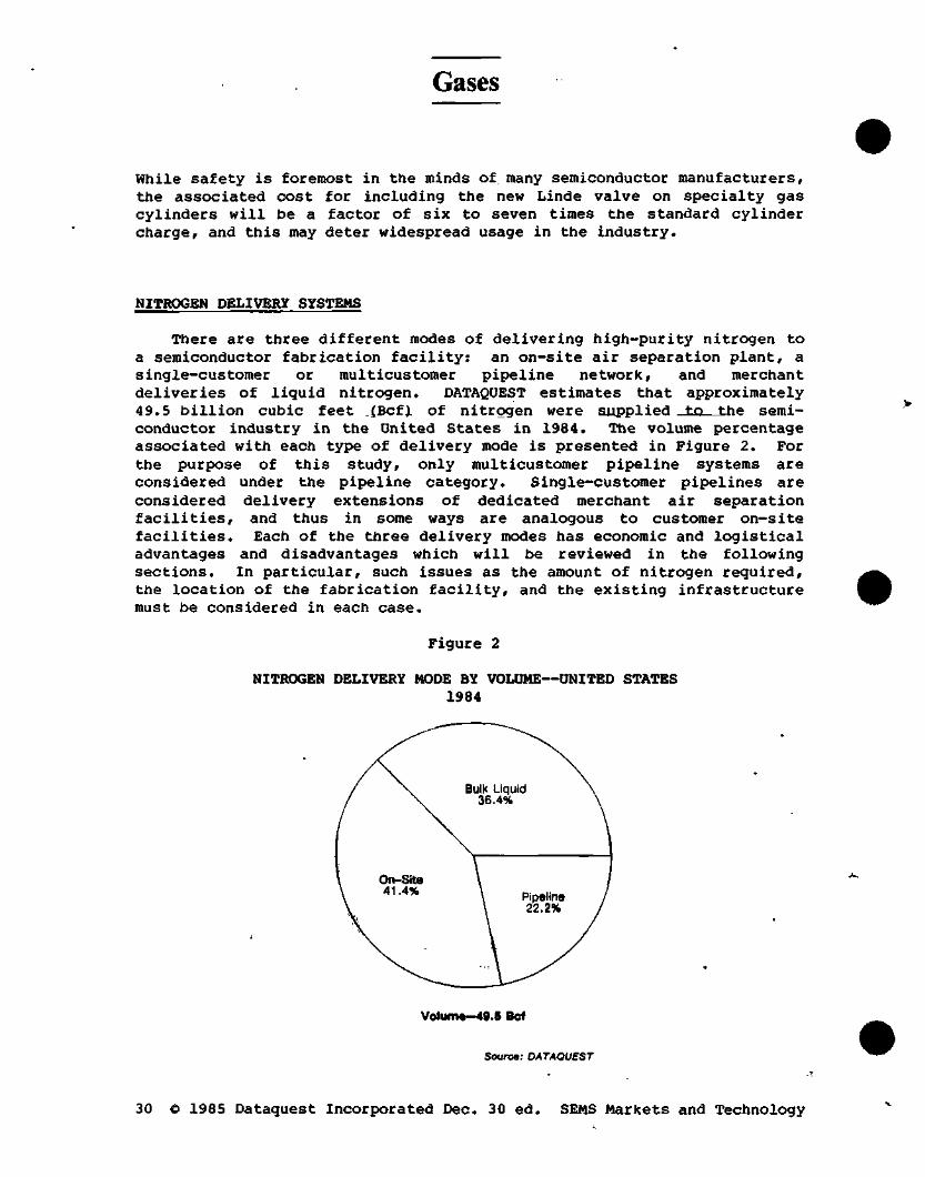
Gases
While safety is foremost in the minds of many semiconductor manufacturers, the associated cost for including the new Linde valve on specialty gas cylinders will be a factor of six to seven times the standard cylinder charge, and this may deter widespread usage in the industry.
NITROGEN DELIVERY SYSTEMS
There are three different modes of delivering high-purity nitrogen to a semiconductor fabrication facility: an on-site air separation plant, a single-customer or multicustomer pipeline network, and merchant deliveries of liquid nitrogen. DATAQUEST estimates that approximately 49.5 billion cubic feet {Bcf). of nitrogen were siipplied _tQ__the semiconductor industry in the United States in 1984. The volume percentage associated with each type of delivery mode is presented in Figure 2. For the purpose of this study, only multicustomer pipeline systems are considered under the pipeline category. Single-customer pipelines are considered delivery extensions of dedicated merchant air separation facilities, and thus in some ways are analogous to customer on-site facilities. Each of the three delivery modes has economic and logistical advantages and disadvantages which will be reviewed in the following sections. In particular, such issues as the amount of nitrogen required, the location of the fabrication facility, and the existing infrastructure must be considered in each case.
Figure 2
NITROGEN DELIVERY MODE BY VOLUME—UNITED STATES 1984
Volunn*-49.5 Bcf
Source: DATAQUEST
30 © 1985 Dataquest Incorporated Dec. 30 ed. SEMS Markets and Technology

Gases
On-site Nitrogen Generation Plants
Semiconductor manufacturers consider an on-site nitrogen generation facility when sufficiently large volumes of nitrogen are required for a given fabrication facility. This occurs when a new facility with large nitrogen consumption requirements comes on-line, or when the consumption of nitrogen has grown beyond the point of economic justification for merchant delivery of liquid nitrogen. Because the consumption rate of nitrogen is substantially larger than that of the other bulk gases, it is the only gas that is economical for a semiconductor manufacturer to produce on-site. One exception, however, is a Texas Instruments facility in Dallas that is supplied via a single-customer pipeline network with high-purity nitrogen, oxygen, argon, and hydrogen generated at a nearby plant operated by Liquid Air. _ _ —
Typically, the gas company responsible for installation of the plant retains ownership and supervises its operation. There are several reasons why this is the case. First, a semiconductor manufacturer has other more pressing demands for capital expenditure than a nitrogen generation plant. In addition, personnel at a fabrication facility are usually not knowledgable about gas production or maintenance of such a facility. Finally, if it becomes necessary to expand nitrogen capacity, existing plant equipment will have to be removed and a larger facility installed in its place, since smaller plants cannot be directly upgraded.
There are several factors that influence the choice for on-site nitrogen generation, but foremost is the wafer production level, and thus nitrogen consumption rate, of a fabrication facility. However, nitrogen consumption in a fab depends on more than just wafer starts, since a certain amount of nitrogen is always required to maintain the processing equipment and environment even when wafer production levels drop. Typically in the industry, it is estimated that 500 to 700 cubic feet of nitrogen are consumed per wafer start, on the average. This figure, which includes both fabrication and maintenance requirements, allows one to calculate the nitrogen consumption rate of a fabrication facility on the basis of wafer starts. If wafer production levels at a given facility decrease, however, the reduction in nitrogen will not drop at the same rate because of the amount of gas that is needed to maintain the integrity of the processing environment.
The consumption rate of nitrogen that economically justifies conversion to an on-site facility is 22,000 to 26,000 cubic feet/hour. This corresponds to approximately 25,000 to 30,000 wafer starts/month if one assumes an average consumption rate of 625 cubic feet of nitrogen/wafer start for 720 hours/month of production operation. By the time a semiconductor manufacturer has reached a nitrogen consumption rate of 28,000 to 30,000 cubic feet/hour (32,000 to 35,000 wafer starts/month), the conversion to on-site nitrogen generation has usually been made.
SEMS Markets and Technology © 1985 Dataquest Incorporated Dec. 30 ed. 31

Gases
Several issues that may affect a lower break-even point for the conversion to an on-site facility include the location of the fabrication facility and the condition of the existing infrastructure. If a semiconductor fab is located in an area that is quite a distance from a merchant source of liquid nitrogen, the additional costs for transporting bulk liquids may become prohibitive when compared with the alternative of on-site nitrogen generation. In addition, if the existing infrastructure (communications and transportation network) is poor, regular and reliable delivery of bulk liquid nitrogen may not be possible, and again, on-site nitrogen generation may be the only alternative. On-site plants at semiconductor fabrication locations have been identified in Israel, Malaysia, and South Korea. In these cases, the infrastructure that would allow for merchant delivery of liquid nitrogen is poor. At the facility in Israel, oxygen and hydrogen as well as nitrogen are produced on-s±tfiu,_ which is unusual since these gases are required in much smaller volumes than nitrogen in the semiconductor processing environment. Hydrogen, oxygen, and argon are rarely produced on-site in the United States because the existing infrastructure is sufficient to make bulk delivery economically viable.
The cost to a semiconductor manufacturer for on-site nitrogen is approximately $0.10 to $0.12/hundred cubic feet (hcf) for an average-size facility (typically 30,000 to 80,000 cubic feet/hour). For a larger facility, the cost may be more like $0.08 to $0.09/hcf. The charge usually includes a regular fixed fee that covers the equipment and facility and the cost of maintaining the plant, as well as the gas itself.
The customer typically pays the power costs for the generation of nitrogen; this can vary considerably, depending on the source of electricity. For example, the energy costs in the Pacific Northwest are several mils per kW-hour (about $0,002 to 0.003/kW-hour) up to $0.01 to $0.02/kW-hour because of the abundant source of cheap hydroelectric power. In the San Francisco Bay Area, however. Pacific Gas & Electric charges $0.07 to $0.10/kW-hour, which makes the overall cost of a customer on-site generation plant prohibitive when compared with the existing pipeline network and liquid bulk deliveries. (Certain discounts on energy rates apply for large-volume users that maintain power consumption at a specified capacity.)
The amount of energy required to generate 100 cubic feet of nitrogen (in liquid form) is approximately 3 kW.-hours, some of which may be recovered from heat exchangers when the liquid is vaporized. Because there is such a wide range in the cost of power, it is very difficult to establish an average selling price for on-site nitrogen that includes these additional on-site fees. For-.the purpose of this study, the average selling price of nitrogen is reported as $0.11/hcf, with the understanding that power charges are not included.
32 © 1985 Dataquest Incorporated Dec. 30 ed. SEMS Markets and Technology

Gases
The current short-term trend is that the number of on-site locations will increase, and that existing locations will continue to add nitrogen generation capacity. However, several industry sources believe that the long-term trend will be away from the large fabrication facilities toward small production centers, and thus the number of new on-site locations will drop dramatically. One disadvantage to on-site nitrogen production that should be mentioned is that regardless of the amount of nitrogen produced at the facility, the fixed fee payments are unaffected. In an economic downturn, such as the industry has recently endured, those fees can become an economic liability for facilities that are required to cut back or shut down production lines.
DATAQUEST estimates that there are more than 50 semiconductor fab locations in the United States that have on-site nitrogen__3eneration facilities, and they account for 20.5 Bcf, or 41.4 percent of total nitrogen consumption in 1984. The major gas companies that provide on-site nitrogen generation facilities in the United States include Air Products, Airco, Liquid Air, and the Linde division of Union Carbide.
On-site nitrogen generation facilities are also found at more than a dozen Japanese semiconductor facilities. Several that have been identified include Fujitsu (Aizu), Matsushita (Arai), Motorola (Aizu), Oki (Miyazaki), a Sharp facility, and Toshiba (Iwate). The companies that supply the nitrogen generation systems include Oaido Sanso, Nippon Sanso, Osaka Sanso, and Teisan.
In the European gas market, several on-site nitrogen generation facilities have been identified in the United Kingdom; generator suppliers for these sites include Air Products, B.O.C., and Petrocarbon (a British supplier of air separation facilities). Limited activity in the area of on-site nitrogen generation plants has also been reported in France and West Germany. Nitrogen on-sites have also been identified in Israel, South Korea, Malaysia, and Singapore. Currently, there is no information available regarding the volume percentage that is accounted for by this mode of nitrogen delivery in Europe, Japan, or countries in ROW.
Pipeline Delivery of Nitrogen
Gaseous nitrogen is supplied to semiconductor facilities via single-customer and multicustomer pipeline networks. For the purpose of this study, however, only multicustomer pipeline systems are considered under the pipeline designation. Single-customer pipelines are considered delivery extensions of dedicated merchant air separation facilities, and thus are analogous to customer on-site :£acilities..
SEMS Markets and Technology © 1985 Dataquest Incorporated Dec. 30 ed. 33

Gases
At this time, there are only three multicustomer pipeline systems that supply semiconductor manufacturers in the United States with nitrogen. While single-customer pipelines exist in Europe as well as Japanf there are currently no multicustomer pipeline networks in those regions. The following discussion, therefore, is limited to the two Air Products pipelines located in the Silicon Valley and Chandler, Arizona, and the new Linde pipeline, located in San Jose, California.
The driving force for establishing a multicustomer pipeline system is the strategic location of a network that has the ability to serve an expanding geographical region of semiconductor production activity. Air Products established its first pipeline system in 1971, located in the Silicon Valley. Over the years, the low-carbon steel pipeline has been expanded to a system that is 25-miles long-r-including—a recent 3-mile extension that is made of electropolished stainless steel. The pipeline network supplies high-purity gaseous nitrogen to more than 45 semiconductor manufacturers in the Silicon Valley, from Mountain View to San Jose, with the recent 3-mile extension into Milpitas. Several major manufacturers that are hooked up to the Air Products' nitrogen pipeline network include Advanced Micro Devices, Fairchild, Hewlett-Packard, Intel, Monolithic Memories, and National Semiconductor. A second Air Products pipeline, also low-carbon steel, was established in Chandler, Arizona, in the late 1970s. It is approximately 25 miles long and serves approximately 10 semiconductor manufacturers, including GTE, General Instruments, Intel, and Motorola.
The Linde division of Union Carbide brought a high-purity nitrogen pipeline system on-line in early 1985. It is a two-mile long stainless steel system that serves the International Business Park in San Jose. There are currently four semiconductor manufacturers that are being supplied with nitrogen from the Linde pipeline network. Linde chose a stainless steel pipeline system rather than low carbon steel because of its ability to provide an ultrahigh-purity, low-contaminant environment for gaseous nitrogen delivery.
DATAQUEST estimates that the volume of nitrogen supplied by multi-customer pipeline networks in the United States was approximately 11.0 Bcf, or 22.2 percent of the total nitrogen volume consumed by semiconductor manufacturers in 1984. This volume is totally attributable to the Air Products' pipeline systems in the Silicon Valley and in Chandler, Arizona, since the Linde pipeline did not come on-line until early 1985. (The Silicon Valley pipeline accounted for 80 percent, or 8.8 Bcf, while the Chandler network supplied the remaining 20 percent, or 2.2 Bcf, of pipeline-delivered nitrogen.) Even for pipeline nitrogen volumes in 1985, the Linde pipeline's contribution to the total amount supplied by multicustomer pipeline systems will be negligible. The cost for nitrogen provided by the pipeline systems varies from $0.20 to $0.24/hcf, with an average selling price of $0.22/hcf.
34 © 1985 Dataquest Incorporated Dec. 30 ed. SEMS Markets and Technology

Gases
Merchant Liquid Nitrogen Delivery
Liquid nitrogen is delivered via tube trailers and tanker trucks to cryogenic holding tanks located "on the pad" at semiconductor manufacturing facilities. This is the only option available for nitrogen supply when a semiconductor manufacturer is not strategically located to take advantage of a multicustomer pipeline system, or if the account is of insufficient size to warrant on-site nitrogen generation. The overwhelming advantage for shipping discrete amounts of bulk liquid rather than gaseous nitrogen is that a single volume of liquid corresponds to an equivalent of 750 volumes of gas after vaporization. Vaporizers are installed on the pad by the gas supplier for on-site conversion from liquid to gas as needed.
The pricing system for merchant delivery of liquid nitrogen can vary considerably depending on the size of the account and the distance of the fab facility from vendor-owned air-separation plants. The basic cost of bulk liquid nitrogen delivery includes the power costs to liquefy and separate out the nitrogen, transportation costs (based on round-trip mileage) to move a discrete volume of liquid by tube trailer to a fabrication facility, as well as a hook-up charge. In addition, there is typically an escalation clause built into the contracts for liquid nitrogen delivery that increases the price of nitrogen as time goes on. (For example, pricing for bulk liquids can in some cases follow the Producer Price Index for Industrial Commodities set by the Bureau of Labor Statistics.) However, as the account grows, appropriate reductions in price are also considered. Thus, taking these many factors into account, the price of bulk liquid nitrogen delivered to a semiconductor manufacturer can vary from as low as $0.17 to $0.19/hcf to $0.50 to $0.60/hcf. In some cases, liquid nitrogen prices in the United States are even greater than $1.00/hcf because of the size/distance factors.
While prices vary considerably, an average selling price of $0.40/hcf is assumed in this study. This cost factor includes delivery of the. bulk liquid as well as the leasing fee for vaporization equipment and storage tanks. Because of very aggressive pricing practices within the gas industry for semiconductor manufacturer accounts, the pricing distribution for liquid nitrogen will continue to span a wide range of values in the future.
The merchant liquid nitrogen delivery prices can be higher overall than either pipeline delivery or on-site generation, even when power costs are included. One reason is that some of the power cost for air liquefaction and separation can be recovered through heat exchange equipment when the liquid is vaporized to a gas. The gas company is
SEMS Markets and Technology © 1985 Dataquest Incorporated Dec. 30 ed. 35

Gases
responsible for the operation of customer on-site facilities, as well as their own plants, and thus can pass the savings in power costs directly on to the semiconductor manufacturer through prices for on-site nitrogen and pipeline-delivered nitrogen. However, with liquid nitrogen delivery, the semiconductor manufacturer is paying for a liquid supply of nitrogen, and thus the cost up front does not reflect any eventual recovery of power charges that may be generated through vaporization.
DATAQUEST estimates that the volume of nitrogen supplied to semiconductor manufacturers in the United States in 1984 from bulk liquid merchant deliveries was 18.0 Bcf, which corresponds to 36.4 percent of the total nitrogen volume consumption.
MARKET ANALYSIS
Worldwide Semiconductor Gas Market
Table 7 presents the worldwide semiconductor gas market in 1984 by regional sales of bulk and specialty gases.
Table 7
1984 WORLDWIDE SEMICONDUCTOR GAS MARKET
Region
United States Japan Europe ROW
Bulk Atmospheric Gases $M Percent
$155.0 46.9% 115.0 34.8 25.0 7.6 35.5 10.7
Specialty Gases $M Percent
$ 50.0 50.0% 42.0 42.0 7.0 7.0 1.0 1.0
Total. $M
$205.0 157.0 32.0 36.5
Percent
47.6% 36.5 7.4 8.5
Total $330.5 100.0% $100.0 100.0% $430.5 100.0%
Source: DATAQUEST
36 © 1985 Dataquest Incorporated Dec. 30 ed. SEMS Markets and Technology

Gases
DATAQUEST believes that specialty gas costs for Japan, Europe, and the ROW are proportionately higher than for the United States because regional gas suppliers do not have full specialty gas manufacturing capability. Thus it is necessary for a variety of different gases to be shipped in cylinders to these areas. For example, DATAQUEST believes that Europe has no dopant manufacturing capability, and that Japan as well may still not have established primary dopant manufacturing. The interrelationships between the various gas companies in different regions of the world provide the necessary distribution networks for such gases.
Table 8 presents the total bulk gas market and the portion of the market represented by nitrogen (revenues, volumes, and average selling prices) for the different regions of the world. Nitrogen is singled out because it is consumed by the semiconductor industry in substantially larger volumes than any of the other gases, and thus represents the majority of the bulk gas market in any given region.
Table 8
COMPARISON OF 1984 WORLDWIDE BULK GAS AND NITROGEN GAS MARKET
Region
United Japan Europe ROW
States
Bulk $M
$155.0 115.0 25.0 35.5
Gas Percent
46.9% 34.8 7.6 10.7
$M
$118.8 88.0 20.0 33.8
Percent
45.6% 33.8 7.7 12.9
Nitrogen Vol(Bcf)
49.5 22.0 10.0 7.5
Percent
55.6% 24.7 11.3 8.4
ASP/hcf
$0.24 0.40 0.20 0.45
$330.5 100.0% $260.6 100.0% 89.0 100.0%
Source; DATAQUEST
Several factors influence the different prices for nitrogen in the different regions of the world, including mode of delivery, infrastructure, and power costs. Nitrogen prices may vary, depending on the mode of delivery, with higher costs for bulk liquid and lower costs for pipeline or on-site nitrogen. DATAQUEST estimates that when the pricing structures
SEMS Markets and Technology © 1985 Dataquest Incorporated Dec. 30 ed. 37

Gases
for the various modes of delivery have been accounted for, the average selling price of nitrogen in the United States is $0.24/hcf. Specific information on the percent of nitrogen supplied by different delivery modes is not available for the other regions.
Prices for bulk liquid and on-site nitrogen are strongly influenced by the variable cost factors associated with distance and quantity for the delivery of liquid, and the power costs associated with operating an on-site plant. DATAQUEST believes that the average selling price for nitrogen in Europe is about $0.20/hcf, strongly influenced by excellent infrastructure, while for Japan and ROW the estimated prices are $0.40/hcf and $0.45/hcf, respectively. Total bulk atmospheric gas costs for the ROW, therefore, are influenced by not only a relatively larger volume of nitrogen because of assembly operation&^ but _a relatively higher cost for the gas as well.
U»S. Semiconductor Gas Market by Product
Table 9 presents the dollar/volume distribution for the bulk atmospheric gases (nitrogen, oxygen, hydrogen, and argon) consumed by the semiconductor industry in the United States in 1984. Nitrogen volumes and average selling prices are also presented by mode of delivery. The revenues represent direct sales of gas to semiconductor manufacturers.
Table 9
1984 BULK ATMOSPHERIC GAS SALES IN THE UNITED STATES BY PRODUCT
Gas
Nitrogen On-site Pipeline Bulk Liquid
Total
Nitrogen Oxygen Hydrogen Argon
Volume (Bcf)
20.50 11.00 18.00
49.50
49.50 1.00 1.10 0.55
Vol %
41.4% 22.2 36.4
100.0%
94.9% 1.9 -2.1 1.1
ASP/hcf
$0.11 $0.22 $0.40
$0.24 $0.60 $1.50 $2.50
$M
$ 22.6 24.2 72.0
$118.8
$118.8 6.0 16.5 13.7
$%
19.0% 20.4 60.6
100.0%
76.6% 3.9 10.6 8.9
Total 52.15 100^% $155.0 100.0%
Source: DATAQUEST
38 © 1985 Dataquest Incorporated Dec. 30 ed. SEMS Markets and Technology

Gases
Average selling prices for the bulk atmospheric gases have a wide range in values because of variable cost factors. These factors include the cost of power to produce the gases through cryogenic air separation and distribution costs that are distance dependent. In addition, there are the delivery and quantity terms, which depend on the relative size and age of the account. In general, average selling prices for nitrogen (per hundred cubic feet) are approximately $0.11 for on-site nitrogen generation facilities (customer pays power), $0.22 for nitrogen pipeline delivery, and $0.40 for bulk liquid nitrogen delivery. The average sellirig price for oxygen corresponds to $0.60/hcf, but can be as high as $1.00/hcf or more. Hydrogen typically costs $1.50/hcf, but the price may range from $1.00 to $2.50/hcf and is highly distance dependent, since there are only a limited number of facilities in the country that produce liquid hydrogen. The average- selling price for argon is approximately $2.50/hcf, but again may vary over a large range of prices from $2.00 to $3.50/hcf, depending on a variety of variable cost factors.
Table 10 shows the specialty gas sales to the semiconductor industry in the United States in 1984 by gas category: silicon-precursors, dopants, plasma etchants, reactant gases, atmospheric purge/cylinder gases, and others. Please refer to Table 1 for the specific gases that ar&—members of each category. The volumes of the different gases consumed in fabrication, as well as their average selling prices, vary considerably. In this study, only revenues associated with each specialty gas category are reported.
Table 10
1984 SPECIALTY GAS SALES IN THE UNITED STATES BY PRODUCT
Gas Category $M Percent
Silicon-Precursors Dopants Plasma Etchants Reactant Gases Atmo/Purge & Others
$17.5 8.0 12.5 5.0 7.0
35.0% 16.0 25.0 10.0 14.0
$50.0 100.0%
Source: DATAQUBST
SEMS Markets and Technology © 1985 Dataquest Incorporated Dec. 30 ed. 39

Gases
O.S. Semiconductor Gas Market by Company
Table 11 ranks the leading bulk gas suppliers by 1984 sales in the United States. Air Products has a substantial share of the bulk gas market with $72 million in sales (46.4 percent share). Air Products' two pipeline networks (in the Silicon Valley and Chandler, Arizona) account for $24.2 million of that $72 million, or 33.6 percent of Air Products' gas revenues from the semiconductor industry. The pipeline systems evaluated on their own correspond to 20.4 percent of the total industry nitrogen revenues, and 15.6 percent of the total bulk gas revenues. Linde is a strong second with 27.1 percent share of the market. Airco and Liquid Air come in at a close tie for third with 13.6 percent and 11.0 percent, respectively. Of the four major gas companies in the United States, only Air Products and Linde have merchant liquid hydrogen manufacturing facilities.
Table 11
1984 BULK ATMOSPHERIC GAS SALES IN THE UNITED STATES BY COMPANY
Company Sales ($M) Percent
Air Products Linde Airco Liquid Air Others
$ 72.0 42.0 21.0 17.0 3.0
46.4% 27.1 13.6 11.0 1.9
Total $155.0 100.0%
Source: DATAQUEST
40 © 1985 Dataquest Incorporated Dec. 30 ed. SEMS Markets and Technology

Gases
Table 12 shows the specialty gas sales in the United States in 1984. The major suppliers of specialty gases to the semiconductor industry include Airco, Union Carbide, Air Products, and Matheson. DATAQUBST estimates that they account for 70 percent of sales directly to semiconductor manufacturers in 1984. Other smaller suppliers include Scientific Gas Products, Liquid Carbonic, and Alphagaz (the specialty gas division of Liquid Air). DATAQUEST estimates that their participation in the market accounts for an additional 16 percent of direct sales to the semiconductor industry in 1984. The remaining 14 percent of sales in 1984 is spread among several companies that typically supply only one or perhaps a handful of the full complement of specialty gases.
Table 12
1984 SPECIALTY GAS SALES IN THE UNITED STATES BY COMPANY
Company Sales ($M) Percent
Airco Linde Air Products Matheson Scientific Gas Products Liquid Carbonic Liquid Air Others
$10.5 9.0 8.0 7.5 5.0 2.5 0.5 7.0
21.0% 18.0 16.0 15.0 10.0 5.0 1.0 14.0
Total $50.0 100.0%
Source: DATAQUEST
Table 13. presents total sales of semiconductor gases (bulk and specialty) in the United States in 1984, and overall market shares for the various suppliers. ~"
SEMS Markets and Technology C 1985 Dataquest Incorporated Dec. 30 ed. 41

Gases
Table 13
1984 TOTAL SEMICONDUCTOR GAS SALES BY COMPANY
Company
Air Products Linde Airco Liquid Air Matheson Scientific Gas Products Liquid Carbonic Others
Sales ($M)
$ 80.0 51.0 31.5 17.5 7.5 5.0 2.5 10.0 „
Percent
39.0% 24.9 15.4 8.5 3.7 2.4 1.2 4.9
Total $205.0 100.0%
Source: DATAQUEST
Japanese Semiconductor Gas Market
The total gas market in Japan in 1984 was $157 million, of which $115 million in sales (73.2 percent) were bulk gases and $42 million in sales (26.8 percent) were specialty gases. The major bulk gas suppliers to Japan's semiconductor industry are Nippon Sanso, Teisan, Oaido Sanso, Osaka Sanso, and Taiyo Sanso. Table 14 shows bulk atmospheric gas sales in Japan in 1984 for these companies.
Table 14
1984 BULK ATMOSPHERIC GAS SALES IN JAPAN BY COMPANY
Company Sales ($M) Percent
Nippon Sanso Teisan Oaido Sanso Osaka Sanso Taiyo Sanso Others
$ 52.0 29.0 8.0 8.0 8.0 10.0
45% 25 7 7 7
_9
Total $115.0 100%
Source: DATAQUEST
42 © 1985 Dataquest Incorporated Dec. 30 ed. SEMS Markets and Technology

Gases
In the specialty gas market, the major suppliers are Nippon Sanso and Seitetsu. Smaller suppliers of specialty gases in Japan in 1984 include Showa Denko, Teisan, and Takachiho. Iwatani, a new entrant in the specialty gas market, did not participate in sales of specialty gases to the Japanese semiconductor industry in 1984. Estimates of market share for the specialty gas suppliers are not presented at this time.
European Semiconductor Gas Market
In Europe, the total 1984 semiconductor gas market was $32 million, of which $25 million in sales (78.1 percent) were bulk gases and $7 million in sales (21.9 percent) were specialty gases. The major gas companies that supply the European semiconductor industry include Air Products, B.O.C, L'Air Liquide/. Linde AG^ Matheson-UCC, MeS5fit_Griesheim, and Union Carbide. (The European operations of Matheson Gas Products are owned by Union Carbide Corporation; thus the designation Matheson-UCC refers to their joint operations.)
The major gas suppliers that serve semiconductor manufacturers in the United Kingdom are B.O.C. and Air Products. In France, L'Air Liquide is the major supplier, while Air Products and Matheson-UCC have smaller shares. In West Germany, the major gas suppliers include Air Products, L'Air Liquide, Linde AG, Matheson-UCC, and Messer Griesheim. In the Benelux region. Air Products and Matheson-UCC are the two major suppliers of semiconductor gases to the area. Estimates of market share by company for the bulk and specialty gas suppliers are not presented at this time.
ROW Semiconductor Gas Market
In 1984, the semiconductor gas market in the ROW was $36.5 million, of which $35.5 million of sales (97.3 percent) were bulk gases and $1 million in sales (2.7 percent) were specialty gases. The ROW countries with significant semiconductor fabrication operations include South Korea and Taiwan, while Malaysia, Hong Kong, and Singapore have substantial assembly operations. The major gas suppliers to these regions, either through direct sales or joint venture agreements, include Nippon Sanso, Teisan, Union Carbide, B.O.C, and L'Air Liquide. Estimates of market share by company for the bulk and specialty gas suppliers are not presented at this time.
Worldwide Nitrogen Market
Nitrogen is consumed by the semiconductor industry in substantially larger volumes than any other gas. 14: is important to understand that nitrogen is used by a semiconductor manufacturer not only in wafer fabrication and assembly, but also to maintain the integrity of the
SEMS Markets and Technology © 1985 Dataquest Incorporated Dec. 30 ed. 43

Gases
fabrication equipment and processing environment. For example, such equipment as furnace banks and some lithography tools, as well as certain types of clean stations, are supplied with a continuous flow of nitrogen, whether wafers are present or not. Therefore, the amount of nitrogen consumed by a semiconductor manufacturer is dependent in some manner on the amount of equipment in a fab as well as on the amount of wafers produced at the facility.
Total worldwide nitrogen consumption by the semiconductor industry in 1984 amounted to 89.0 Bcf (see Table 8). Figure 3 presents worldwide nitrogen consumption as well as worldwide silicon consumption by region for 1984. (Silicon consumption in the United States includes captive as well as merchant manufacturers.)
At first glance, the distribution of nitrogen by region presented in Figure 3 does not appear to correlate with total semiconductor production as measured by million square inches of processed silicon, particularly in a comparison between the United States and Japan. It appears that Japan uses quite a bit less nitrogen relative to its silicon consumption than the United States. In addition, assembly operations, which consume nitrogen, are retained onshore in Japan, while DATAQUEST estimates that 85 percent or more of assembly operations for U.S. semiconductor manufacturers are performed offshore (in the ROW).
Figure 3
1984 WORLDWIDE NITROGEN AND SILICON CONSUMPTION
ROW 3.4%
Total Silicon—1,769 Million Square Inches Total Nitrogen Volunne—89.0 Bcf
Source: DATAQUEST
44 © 1985 Dataquest Incorporated Dec. 30 ed. SEMS Markets and Technology

Gases
DATAQUEST believes that the difference in nitrogen consumption can be accounted for in part by a difference in philosophy of manufacturing operations. DATAQUEST believes that Japanese semiconductor manufacturers follow very tight regulations in nitrogen flow rates for processing equipment, whether in wafer fabrication production or in maintenance mode. In the United States, however, DATAQUEST believes that there is a tendency for a larger acceptable tolerance in nitrogen flow rates, in particular for flow rates to slowly increase over time. When it is recognized that nitrogen consumption has become unacceptably high in a given fabrication facility, flow rates are reduced to acceptable levels. However, the gradual increase in nitrogen consumption may be repeated in the absence of strict supervision in the processing environment.
There are other factors that may also account -for the -d-i^erence in nitrogen consumption in Japan and the United States relative to semiconductor production. The first factor to consider is product mix and its influence on consumption of nitrogen. The Japanese semiconductor industry produces a relatively larger number of discrete and linear devices than the United States. These devices do not require the same level of processing as some of the more advanced devices, and therefore do not require as much nitrogen per wafer.
A decrease in nitrogen consumption is influenced by the trend toward the usage of clean dry air (CDA) in those applications that do not require a nitrogen environment. The substitution of CDA for nitrogen in certain applications (dessicators, pneumatic-actuated valves, some lithography tools) has been adopted by some semiconductor manufacturers in the United States; however, the trend can at best be described as gradual. DATAQUEST is uncertain of the amount of CDA that is currently being used in Japanese facilities.
Other trends that correlate with a decrease in nitrogen consumption include an increase in the use of argon for annealing, as well as an increase in ion implantation over diffusion. DATAQUEST believes that Japanese semiconductor manufacturers purchased more ion implantation equipment than the United States in both 1983 and 1984. The Japanese therefore have a substantially larger focus on ion implantation than U.S. manufacturers when taken in comparison with the amount of silicon processed in each region. DATAQUEST believes that a combination of these factors account for the difference in nitrogen consumption in Japan compared with the United States, relative to their respective levels of semiconductor production.
The large consumption of nitrogen in the ROW includes not only that area's semiconductor production but the substantial assembly operations in Pacific Rim countries. DATAQUEST estimates that 85 percent or more of U.S. assembly and 90 percent of European assembly occurs offshore, and the nitrogen consumed in ROW takes into account those assembly-related nitrogen requirements.
SEMS Markets and Technology © 1985 Dataquest Incorporated Dec. 30 ed. 45

Gases
The various factors that we believe will affect future nitrogen consumption by semiconductor manufacturers in addition to wafer starts are summarized in Table 15.
Table 15
FACTORS INFLUENCING FUTURE NITROGEN CONSUMPTION
Increases in Nitrogen Usage
• Shift toward larger-sized wafers
• Increase in nitrogen consumptioii for United-States .and—Europe as assembly operations return onshore
• Increase in the installed equipment base with accompanying requirement for nitrogen to maintain integrity of processing equipment and environment
Decreases in Nitrogen Usage
• Trend toward ion implantation and away from diffusion
• Increased use of clean dry air for noncritical applications such as dessicators, pneumatic-actuated valves, and lithography equipment (e.g., aligners and track equipment)
ii Trend toward use of argon in annealing rather than nitrogen (in particular for thin gate oxides)
• Decrease in nitrogen in ROW as assembly operations return onshore for the United States and Europe
Trends in Nitrogen Delivery Mode
• Areas with traditionally poor infrastructure, such as ROW, will continue to go to on-site nitrogen facilities
• U.S. in general experiencing trend toward smaller fabs; thus, trend will be toward more bulk liquid delivery of nitrogen
• Geographical concentrations of-, existing and future semiconductor production will be advantageous sites for multicustomer pipeline networks
Source: DATAQUEST
46 © 1985 Dataquest Incorporated Dec. 30 ed. SEMS Markets and Technology

Gases
since nitrogen flow is used to maintain the integrity of many pieces of processing equipment during times of nonpreduction, the nitrogen market exhibits surprising stability during economic downturns in the semiconductor industry. DATAQUEST estimates that nitrogen consumption in the United States is only down 10 percent by volume in 1985, from 49.5 Bcf in 1984 to 44.5 Bcf. The corresponding decrease in million square inches of processed silicon from 1984 to 1985 is 35 percent from 834 million square inches to 542 million square inches. DATAQUEST believes that because nitrogen is such a large portion of the bulk gases market, both by volume and dollar value, that gas companies, in general, represent one of the few industries with the ability to weather the economic roller coaster of the semiconductor industry.
Worldwide Semiconductor Gas Market Forecast
Table 16 contains DATAQUEST's forecast for bulk and specialty gas sales by region from 1985 through 1990. The sales of semiconductor gases in 1984 are also included in the table. CAGR refers to compound annual growth rate.
DATAQUEST believes that in general, the consumption of the bulk atmospheric gases oxygen, argon, and hydrogen, as well as the specialty gases, will follow the trend in consumption of silicon by the semiconductor industry. However, as mentioned previously, the consumption of nitrogen is dependent not only on wafer starts but also on the installed base of equipment in fabrication facilities. The nitrogen market therefore is not as sensitive to the economic cycles of the semiconductor industry as the other gases, which are considered as direct consumable materials in wafer fabrication.
The pricing forecast for all of the bulk atmospheric gases will be influenced by the cost of power to produce them and transportation costs to distribute them. In addition, argon pricing will continue to rise in response to decreased oxygen production by the gas companies for industries outside of the semiconductor industry, in particular the steel industry. Argon is a byproduct in oxygen separation, and when oxygen demand from the steel industry was high, sufficient amounts of argon were produced to amply supply the semiconductor industry. With decreased oxygen requirements from a declining steel industry, gas manufacturers have found it necessary to run facilities for argon production alone, which is reflected in higher argon prices.
SEMS Markets and Technology © 1985 Dataquest Incorporated Dec. 30 ed. 47

Gases
Table 16
WORLDWIDE SEMICONDUCTOR GAS MARKET FORECAST 1984-1990
(Millions of Dollars)
Region
United States BAG* SPG**
Japan BAG SPG
Europe BAG SPG
ROH BAG SPG
Total BAG SPG
1984
$155.0 50.0
115.0 42.0
25.0 7.0
35.5 1.0
$330.5 $100.0
1985
$131 34
108 36
24 6
33 1.4
$296 $ 77
1986
$153 44
124 44
29 8
41 1.9
$347 $ 98
1987
$195 62
167 64
37 12
58 3.2
$457 $141
1988
$244 81
218 90
50 17
79 5.0
$591 $193
1989
$261 79
237 97
57 20
90 6.3
$645 $202
1990
$
$ $
318 101
293 127
72 26
114 9.0
797 263
1984-1990
12.7% 12.4%
16.9% 20.2%
19.3% 24.4%
21.5% 44.2%
15.8% 17.5%
Total $430.5 $373 $445 $598 $784 $847 $1,060 16.2%
*Bulk atmospheric gases **Specialty gases
Source: DATAQUEST
A system for argon reclamation has recently been developed by Coke Process Systems, Inc. (Westborough, Massachusetts) for efficient recovery and purification of argon used in silicon crystal growing operations. ARCO Solar (Camarillo, California), which manufactures silicon for solar cell applications, will have one of the first systems installed and operational by April 1986. If the claims of 80 percent recovery and higher-purity argon are realized, argon reclamation systems could have a substantial impact on the gas industry in the coming years.
48 © 1985 Dataquest Incorporated Dec. 30 ed. SEMS Markets and Technology

Gases
In the forecast for specialty gases, the costs associated with the different specialty gas categories have not been assigned. The use of plasma etchants, however, will continue to increase as the industry focuses on dry etching for smaller geometry devices. The dopant market will see some decrease in usage over time as the trend continues toward ion implantation, which uses less material than the alternative method of diffusion. Tungsten hexafluoride usage will continue to gain a share of the specialty gas market because of the development of the Genus CVD reactor for the deposition of tunsten silicide.
Semiconductor Gas Market Regional Comparison, 1984 and 1990
Figures 4 and 5 represent^ percent bulk and specialty gas sales by region for 1984 and 1990, respectively. The United States and Japan are expected to have equal shares of the worldwide semiconductor gas market in 1990, with each region responsible for approximately $420 million in gas sales. However, DATAQUEST expects that Japan will overtake the United States in consumption of silicon by 1987, and that the equal size of the respective gas markets in 1990 can be accounted for by the continued efficient utilization of nitrogen in Japan, as described previously. Europe and ROW will have also increased their share of the semiconductor gas market in 1990 over their respective shares in 1984 at the expense of the U.S. market. The increase in the Japanese, European, and ROW gas markets reflect increased silicon consumption and production of semiconductor devices relative to the U.S. semiconductor industry.
In 1984, specialty gas costs in Japan, Europe, and ROW for a given volume of gas were comparatively higher than those for the United States because of the necessity to ship gases into those regions lacking primary manufacturing capability. DATAQUEST believes that primary manufacturing of specialty gases will become more prevalent in Japan, Europe, and ROW, and therefore prices for specialty gases will become more comparable with those in the United States by 1990.
The bulk gas market in the ROW will still reflect the additional nitrogen required for assembly operations of U.S. and European devices. However, DATAQUEST believes that onshore assembly operations will continue to grow in these two regions.
SEMS Markets and Technology © 1985 Dataquest Incorporated Dec. 30 ed. 49

Gases
Figure 4
1984 WORLDWIDE SEMICONDUCTOR GAS MARKET BY REGION
Total Sales-$430.5 Million
Figure 5
ESTIMATED 1990 WORLDWIDE SEMICONDUCTOR GAS MARKET BY REGION
Total Sales—$f,'060 Million
Source: DATAQUEST
50 ® 1985 Dataquest Incorporated Dec. 30 ed. SEMS Markets and Technology

Gases
GENERAL CONCLUSIONS
DATAQUEST believes that the semiconductor gas market will continue to remain price and quality competitive. There are few players in the market, and each is determined to maintain its customer base within the semiconductor industry because of the perceived importance of participating in the growth of high-technology industries. As each new semiconductor fab comes on-line, all major suppliers will participate in bidding for new contracts, and thus pricing structures will reflect the competitive drive for future market share.
In addition to competing on the basis of price, the gas companies are also focusing on the timely issues of quality control and customer support. The gas industry no longer _supplies just one —o£—the many consumable materials used in wafer fabrication, but rather offers a complete package from the gas itself to the associated gas-handling equipment to technical support at the semiconductor manufacturer's facility. The gas companies are developing integrated quality control systems from point of manufacturing to point of delivery to point of use. We believe that purity, efficient filtration systems, and quality control for gases will remain of paramount importance as semiconductor manufacturers continue to emphasize reduced particulate and contamination levels in their quest for VLSI devices and beyond.
SEMS Markets and Technology © 1985 Dataquest Incorporated Dec. 30 ed. 51


Automated Assembly Model
OVERVIEW
This chapter deals with the design and manufacturing cost analysis of a domestic automated IC assembly facility. The facility is characterized by high-volume, standard processing, and low-labor assembly, and would therefore be more representative of a large IC manufacturer than a small-volume or contract assembler. The model assumes the highest level of automation obtainable today from merchant equipment suppliers.
A discussion of future developments in assembly technology is also included.
Because of the use of automated equipment wherever possible, the facility is heavily capitalized, and fixed costs represent a large portion of unit cost. Although labor rates are rising steadily in many overseas countries where IC assembly is common, and automation may be considered a substitute for labor, the fully automated plant may not be justifiable by payback methods for several years. The current emphasis on automating assembly is not driven by expected savings of direct labor costs.
Rather, automation is a response to the increasing need for quality assembly. Many manufacturers assert that assembly yield and product reliability of automatically assembled devices far exceeds that of manually assembled parts. The leading Japanese IC manufacturers have demonstrated excellence in product quality; this is partially attributable to their high level of automation. Process control is the key to high-speed, consistent processing. In addition to improving the independence, speed, and consistency of assembly equipment, much attention is currently centered on making advancements in CAM as a process-optimization tool and in the diagnostic and feedback capabilities of assembly equipment as it interfaces to a CAM network.
Of course, cost savings do result from yield improvements gained by automation, and these savings are most significant for high ASP (average selling price) devices and high pin-count devices. For the former, each device gained in yield represents a relatively large dollar amount. For the latter, yield improvements themselves are large because automatic bonding greatly increases throughput and yield at bond.
As automated equipment matures and becomes more affordable, the justification for automating low lead-count devices will increase. For these devices, labor and overhead are the major determinants of device cost, and these are still minimized in offshore high-labor operations.
SEMS Markets Technology © 1986 Dataquest Incorporated April 15 ed.

Automated Assembly Model
WHY ONSHORE?
Onshore assembly allows faster turnaround, closer process control, and better engineering/manufacturing interface than offshore assembly. These factors all have a positive effect on product quality and customer service. Some economic benefits also result from onshore operation.
Turnaround
Faster turnaround is achieved onshore with automated processing due to the elimination of shipping time, customs procedures, and communications delays. A realistic estimate for cycle time reduction for products built onshore is one week, considering that shipping to the Far East requires two days in each direction and customs clearances often require one day. If a manufacturer is shipping against backlog, then every unnecessary day in the manufacturing cycle costs him interest on revenue. Cycle time reductions represent savings in interest applied to the selling price of the device, as well as the materials used in its construction. In addition, onshore assembly allows the domestic manufacturer of wafers to maintain a lower inventory of wafers in the "die bank" preceding assembly, because he does not have to bear the uncertainty of shipping and customs delays in his supply of material. Offshore die banks commonly hold a 10 to 15 day supply of wafers, while onshore manufacturers can manage with 3 to 5 days of backup inventory. The holding costs associated with this inventory of wafers can be quite significant; a rough estimate of the savings that would result from a seven-day reduction in wafer inventory for the RAM assembly facility modeled in this section is $989 per operating day, or $259,528 annually (calculated using 13 percent interest rate). It is clear that from the standpoint of cycle time cost reductions, there is much justification for onshore assembly of high ASP devices.
Process Control
Closer process control and better engineering/manufacturing interface are the benefits of locating process and product engineering at the manufacturing site. This allows engineering to monitor the effects of process changes in the manufacturing environment, and to implement such changes smoothly. And with the faster turnaround, process problems can be spotted more quickly, before several weeks of WIP (work in process) become involved. These two factors produce the desired incremental improvements in yield and average product quality.
#
2 © 1986 Dataquest Incorporated April 15 ed. SEMS Markets Technology

Automated Assembly Model
Onshore Plants
Several major IC manufacturers have recently made commitments to large-scale automated facilities onshore. Motorola began operations in a new Chandler, Arizona, assembly and test facility in 1983. Intel is currently building an assembly and test facility in Chandler, where its corporate assembly and test group is located, to start up in 1985. This plant will utilize just-in-time delivery and will serve as a test site for new manufacturing equipment and processes. Fairchild has combined state-of-the-art automated equipment and its internally developed CAM system, INCYTE, at its South Portland, Maine, site to drastically reduce the labor required in assembly. Even some of the Asian subcontractors, notably Anam, Stanford Microsystems, and Dynetics, are considering opening U.S. facilities to serve their client bases here. Cypress has been successfully running high volume operations in San Jose, California, for several years.
An Economic Conqpar ison
Traditionally, onshore production has been considered prohibitively expensive by IC makers. A discussion of the tradeoffs may shed some light on the economic issues. If automated assembly is the goal, equipment depreciation costs will be the same for onshore and offshore. Construction costs are comparable, and facilities costs may be higher overseas depending on location. So, fixed costs do not represent a strong argument for either case. Material costs are not dependent on location. Labor costs are a major advantage for offshore assembly, although availability of skilled labor to maintain automated equipment overseas may be a difficult problem. Elimination of freight and exporting charges, legal costs of exporting, and communications charges, plus cycle time cost reductions discussed earlier, are economic advantages not always considered when comparing onshore and offshore costs. These narrow the gap and may even close it, depending on such factors as device size and costs, site country under consideration, and service networks utilized. However, industry consensus is that offshore assembly still enjoys a slight cost advantage over onshore, and this will be true for at least a few more years.
PRODUCTIVITY CONSIDERATIONS
Organization
The assembly facility is intended to produce a maximum output and also to provide an environment for process optimization work. Accordingly, manufacturing is a three-shift-per-day, five-day-per-week
SEMS Markets Technology O 1986 Dataquest Incorporated April 15 ed.

Automated Assembly Model
operation and manufacturing personnel, including operators, supervisors, quality assurance inspectors, and facility and maintenance technicians cover three shifts. Product and process engineering interface with manufacturing during the day shift. All personnel report to the line manager who holds the responsibility for setting and meeting goals in the areas of product quality level and assembly yields, and keeping abreast of current technology. A typical organization chart is shown in Figure 1.
The assembly group consists of assembly operators and assembly supervisors. Although an operator is usually trained and certified to run several stations on the line, he typically performs one function during a shift rather than accompanying a batch of material through the line. Much of the operator's work involves keeping a station supplied with material, loading and unloading the input and output when necessary, logging the flow of material through that point in the line, and transporting finished material to the next point. He or she has been trained in operation of the equipment, and monitors it for malfunctions requiring maintenance attention. Each supervisor is responsible for managing a section of the process; he or she schedules material movement through the line and can shut down a station for unscheduled maintenance if it runs outside the assembly specification.
The facilities and equipment maintenance staff has the responsibility for ensuring optimum performance of the equipment and facilities networks such as water and power supply. Technicians perform scheduled maintenance on equipment and any necessary changeovers of transfer and indexing systems unique to device types. They also repair and tune equipment that has malfunctioned or wandered outside operating specifications.
Figure 1
ORGANIZATION CHART
Line Manager
Assembly Product and
Process Engineering
Facility and Equipment
Maintenance
Source: DATAQUEST
O 1986 Dataquest Incorporated April 15 ed. SEMS Markets Technology

Automated Assembly Model
Quality assurance performs selective inspections of output to ensure that the product meets specifications at each step in the process and at the final visual stage. The frequency and extent of inspection is usually determined by sampling plan theory. If lots fail the QA inspection on these terms, they may require 100 percent visual inspection. This should prove necessary for less than 5 percent of the lots. QA personnel may also perform tests such as bond pull or solderability to accept lots on a quality basis.
Another very important function of QA is incoming inspection of assembly materials. This is to ensure that material quality and consistency is sufficient for use in the specified processes, and is becoming more critical as processing speed and equipment sensitivity increase.
Product and process engineers provide the specifications for device assembly. They develop and install new processes, train operators to run the various assembly stations, and take responsibility for the quality of material produced. Because IC processing requires knowledge pertaining to device characteristics, material properties, and equipment capability, this group usually consists of a mix of electrical engineers, mechanical engineers, material engineers, and chemists.
Equipment Selection Criteria
The range of choices of equipment has been broadening as European and Japanese vendors extend their product offerings to the U.S. market. In addition, many large IC producers, including Texas Instruments and Fairchild, internally develop machines with the goals of meeting a special need or improving upon what is available on the open market. Many assemblers also work with equipment vendors to customize standard models by creating interfaces between stations or adapting load/unload mechanisms to the assembler's magazine.
Each manufacturer's criteria for equipment selection vary with his unique constraints, including product mix and available resources. Maintaining a high utilization of equipment is key to cost-effective assembly. Some equipment is optimally used in a dedicated fashion and can run very high volumes without maintenance or adjustment. Other equipment offers flexibility in changeover between device types or pin counts and is more efficient for the small volume manufacturer or subcontractor, but is often less fully automated. For example, one plate mold can be used for semiautomatic encapsulation of 8, 14, 16, and 20 pin DIP'S in the 300 mil family, but offers lower throughput than a fully automated mold system.
SENS Markets Technology o 1986 Dataquest Incorporated April 15 ed.
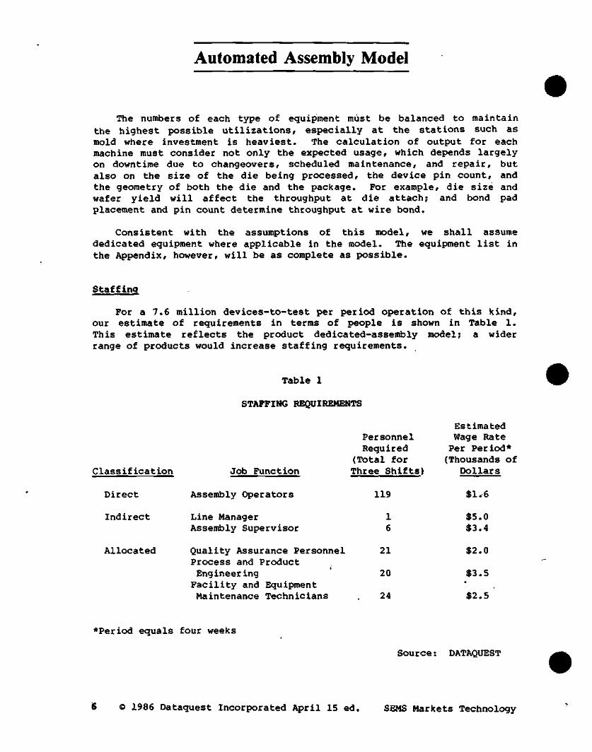
Automated Assembly Model
The numbers of each type of equipment must be balanced to maintain the highest possible utilizations, especially at the stations such as mold where investment is heaviest. The calculation of output for each machine must consider not only the expected usage, which depends largely on downtime due to changeovers, scheduled maintenance, and repair, but also on the size of the die being processed, the device pin count, and the geometry of both the die and the package. For example, die size and wafer yield will affect the throughput at die attach; and bond pad placement and pin count determine throughput at wire bond.
Consistent with the assumptions of this model, we shall assume dedicated equipment where applicable in the model. The equipment list in the Appendix, however, will be as complete as possible.
Staffing
For a 7.6 million devices-to-test per period operation of this kind, our estimate of requirements in terms of people is shown in Table 1. This estimate reflects the product dedicated-assembly model; a wider range of products would increase staffing requirements.
Table 1
STAFFING REQUIREMENTS
Classification Job Function
Personnel Required
(Total for Three Shifts)
Estimated Wage Rate Per Period* (Thousands of
Dollars
Direct Assembly Operators
Indirect Line Manager Assembly Supervisor
119
1 6
$1.6
$5.0 $3.4
Allocated Quality Assurance Personnel 21 Process and Product Engineering 20 Facility and Equipment Maintenance Technicians 24
$2.0
$3.5
$2.5
*Period equals four weeks
Source: DATAQUEST
1986 Dataquest Incorporated April 15 ed. SEMS Markets Technology

Automated Assembly Model
ASSEMBLY LAYOUT AND FACILITY REQUIREMENTS
Introduction
In this section we describe the main process flow used for assembling plastic encapsulated packages, list the needed equipment, show an example of equipment layout in the assembly area, and describe the facility requirements.
Laying out a production assembly area requires balancing of often-contradicting needs. The requirements are similar to those considered in fab design. These objectives are to:
• Ensure a smooth flow of material through the sequence of assembly operations
• Allocate space and equipment for new technology developments so that this activity will not interfere with standard production.
• Simplify the layout of piping, air, and exhaust ducting and power distribution for ease of maintenance and minimal construction cost
• Facilitate equipment maintenance, so that it will not disturb work on all equipment
• Isolate "dirty" back-end processes such as mold, trim and form, and solder dip from cleaner front-end processes such as wafer saw, die attach, and wire bond to minimize particulate contamination
Utilization of the clean area is left as an option to the reader. IC makers vary from no clean room use at all to full utilization, including back-end processing. One intermediate approach is local clean areas achieved with laminar flow hoods. It seems a general rule, however, that front-end processing is separated from or protected from the contamination generated in the back end. We represent this isolation by physically dividing assembly into two areas.
Process Flow
The plastic processing flow is a well-established one. The outline shown in Table 2 is fairly standard with the exception of lead finishing. Lead plating before trim and form is also common practice;
SEMS Markets Technology O 1986 Oataquest Incorporated April 15 ed.

Automated Assembly Model
some manufacturers produce both plated and dipped parts. We have chosen to use solder-dipped parts for two reasons:
• In general, dipping is associated with less contamination than plating and is more consistent with the high automation and reliability goals modeled.
• The model's product mix includes a surface-mounted product on which users prefer to have the thicker solder coat that is provided by dipping.
Table 2
PLASTIC ASSEMBLY PROCESS FLOW OUTLINE
Process Step
Incoming
Wafer Mount
Saw
Die Attach
Epoxy Wire
Wire Bond
Mold/Mold Cure
Deflash
Trim and Form singulate devices
Label
Lead Finish
QC—Rework
Outgoing
Function
Receive and log in wafers from fabrication
Affix probed wafer onto taped frame
Scribe wafer into dice
Mount good die onto leadframe bar pad
Cure die attach paste
Form electrical connection between chip I/O and leadframe with gold wire
Encapsulate bonded device in thermoplastic
Remove residual resin on leadframe surface from mold
Remove extra metal from leadframe; form leads and"
Mark vendor and device identification on part
Solder coat leads
Inspect parts for visual defects; rework label or lead finish and straighten leads
Document lot statistics and ship to Burn-In/Test area
Source; DATAQUEST
8 © 1986 Dataquest Incorporated April 15 ed. SEMS Markets Technology

Automated Assembly Model
Equipment List
The list of equipment necessary for performing all the required process steps is given in the appendix at the end of this section, with representative prices, delivery times, and manufacturers. Only merchant manufacturers of fully automatic equipment are listed; semiautomatic and manual equipment available on the market is not listed and neither are exclusively captive manufacturers.
It should be noted that price and delivery time vary somewhat with manufacturer and with options desired; therefore the information listed for the processes of this model may not be applicable in every case.
The estimates of yield by process step used in calculating capacity and equipment requirements are shown in Table 3. They are theoretical allocations of the overall assembly yield, which is determined at room-temperature testing. Conservative utilization figures for each equipment group were used to allow for maintenance required to maintain optimum performance. The total equipment cost for the model facility of 98.8 million devlces-to-test per year capacity was approximately $5 million.
One notable exemption on the equipment list is a CAM (computer-aided manufacturing) system, which is a necessity in state-of-the-art production facilities. The choice of system is left to the reader and depends of various factors such as the form of engineering analysis desired and hardware preferences. The cost of a complete CAM system can easily run to $800,000; a typical breakdown would be $50,000 for a CPU, $150,000 for peripheral hardware, $100,000 to $200,000 in software, and $400,000 for In-house installation costs. Installation and optimization of a system into a manufacturing environment can require two years or longer.
SEMS Markets Technology o 1986 Oataquest Incorporated April 15 ed.

Automated Assembly Model
Table 3
DEVICE MECHANICAL YIELD
Operation
Wafer Mount
Wafer Saw
Die Attach
Wire Bond
Mold
Trim and Form
Label
Lead Finish
Overall Assembly Yield
Yield (Percent)
100.0%
100.0%
99.5%
99.0%
99.5%
99.5%
100.0%*
100.0%*
Cumulative Yield
(Percent)
100.0%
100.0%
99.5%
98.5%
98.0%
97.5%
97.5%
97.5%
97.5%
Number of Starts Per Week
1,949,612
1,949,612
1,949,612
1,939,864
1,920,465
1,910,863
1,901,309
1,901,309
Devices-To-Test Per 4-Week Period—7,605,235
*With rework
Source: DATAQUEST
Assembly Layout
A typical layout for the equipment in the assembly area is shown in Figure 2. The figure illustrates the islands automation arrangement typical today. As robotic capability increases, and operations are tied together with automatic interfaces, an in-line arrangement may become more effective.
As discussed earlier, the front end is separated from the back end to allow for cleaner processing of the chip. Material transport is still performed by humans but only in bulk form. Ideally, a standard magazine holding several hundred leadframes is used at all stations for loading and unloading so that no direct human handling of the materials being assembled is necessary.
10 © 1986 Dataquest Incorporated April 15 ed. SEMS Markets Technology

Automated Assembly Model
Figure 2
ASSEMBLY AREA LAYOUT
PnbMl
W*l»n
DWIOM loTMt
WalM^ Mount
OC OSM
J
Witr Saw
^
Wafw W u h
TraiMport
MmBond
IMU
QCVittMl
SoldwCHp
SotdwOip
OC (tf^it^
OC
\
Cum
Cura
Trim and Form •
11
CMlMh
CMlMh a
OATAOUEST
SENS Markets Technology o 1986 Dataquest Incorporated April 15 ed. 11

Automated Assembly Model
Facility Requirements
The assembly area requires installed services to supply DI water, liquid nitrogen, pressurized air, and hydrogen, in addition to standard utilities. The costs of these installations is included in the construction costs listed under fixed costs in Table 4. For accounting purposes, we have assumed that this cost is covered at one time as a nonrecoverable leasehold improvement rather than over time in the form of an allowance against rental fees.
Table 4
LABOR COSTS (Thousands of Dollars)
Personnel
Direct: Assembly Operators
25 Personnel Percent Total
Wage Cost Per Fringe Personnel Number Rate Period Benefit Cost
119 $1.6 $190.4 $47.60 $238.00 •
Indirect: Line Manager Assembly Supervisor
1 6
$5.0 $3.4
$ 5.0 $ 20.4
Total Indirect $ 25.4 $ 6.35 $ 31.75
Allocated: Quality Assurance Personnel Process and Product Engineering Facility and Equipment Maintenance Technicians
Total Allocated
21
20
24
$2.0
$3.5
$2.5
$ 42.0
$ 70.0
$ 60.0
$172.0 $43.00 $215.00
Source: DATAQUEST
12 © 1986 Dataquest Incorporated April 15 ed. SEMS Markets Technology

Automated Assembly Model
ASSEMBLY COSTS ANALYSIS ASSUMPTIONS
The assumptions described in previous sections are:
• Production
- High volume (7.6 million devices-to-test per four-week period)
Three full shifts in assembly
- Personnel requirements, wage rates, and labor costs for direct, indirect, and allocated personnel as shown in Table 5
Mature operation in steady-state mode
• Yield; Overall assembly yield is 97.5 percent
• Technology
Fully automated processing by station
Standard plastic processing
Five-inch wafer
Solder dip lead finish
The product mix used to calculate resource requirements was chosen to optimize the effectiveness of onshore automated assembly. A product mix of approximately one-third each 64K DRAMs in a 16-pin DIP, 64K DRAMs in an 18-pin chip carrier, and 256R DRAMs in a 16-pin DIP was found to represent a high-volume product that requires standard processing but still commands a fairly high average selling price.
Assembly yield is assumed to be sufficient to eliminate the second optical and third optical inspection stations historically found after die attach and wire bond, respectively. Instead, QC gates after each major process step sample material to monitor product quality.
SEMS Markets Technology O 1986 Dataquest Incorporated April 15 ed. 13

Automated Assembly Model
Table 5
ASSEMBLY COST ANALYSIS
Fixed Costs Per Period (Four Weeks)
Rent (20,000 Square Feet at $0.60 per square feet) Power Gases Water
Depreciation:
Assembly construction (120 months); $900,000 Other construction, including office and rest area (120 months); $240,000
Assembly equipment, excluding CAM system (60 months); $4,977,300
Total Per Calendar Month Total Per Period
Cost Per Device Out
$ 12,000 $ 28,500 $ 6,500 $ 750
$ 7,500
$ 2,000
$ 82,955
$140,205 129,420
$ 0.017
Variable Costs Per Period
Material Cost Per Device (Yielded):
Leadframe (stamped, silver spot) Mold Compound Epoxy Gold Wire
Cost Per Device Out
Labor Cost Per Period:
Direct Indirect Allocated
Total Per Period
Cost Per Device Out
Source:
$ 0.035 0.016 0.006 0.006
$ 0.063
$238,000 31,750 215,000
$484,750
$ 0.064
DATAQUEST
14 © 1986 Dataquest Incorporated April 15 ed. SEMS Markets Technology

Automated Assembly Model
FIXED COSTS
Facilities
We assume that the building is rented as a shell at $.60 per square foot per month. The space rented consists of 12,000 square feet of assembly area and 8,000 square feet for offices and service, totaling 20,000 square feet. Facility design is contracted to an outside engineering firm and all facilities and services are supplied from scratch.
Table 4 shows that the average cost of construction and equipment of the systems supporting the assembly area is $900,000. The cost of nonmanufacturing area construction, which includes office space, eating area, rest rooms, etc., is $240,000. The sum of $1,140,000 represents the total permanent or nonrecoverable investment in the rented shell, and is depreciable over a ten-year period.
Equipment
The appendix to this section shows that equipment costs for the assembly area total $4,977,300. Such costs can normally be depreciated over a five- to seven-year period; due to the high-technology nature of the equipment, we have assumed the shortest possible depreciation period, or five years.
The packaging cost per device out, exclusive of chip cost, based on all fixed costs and variable costs of materials and labor, is shown as a percentage of the total cost:
Fixed Cost Per Device $0,017 11.4% Assembly Materials $0,068 45.6 Assembly Labor $0.064 43.0
$0,149 100.0 I
Fixed costs represent a relatively high portion of the yielded device cost in this model due to the heavy investment in automated equipment. As automation capability in handling and inspection grows, this sector will gain a share of the cost from the labor cost sector. However, labor will always occupy a significant place in assembly cost in the form of skilled labor; engineering and maintenance personnel will contribute to the automation process and displace direct labor personnel.
SEMS Markets Technology O 1986 Dataquest Incorporated April 15 ed. 15

Automated Assembly Model
FUTURE DEVELOPMENTS IN ASSEMBLY TECHNOLOGY
DATAQUEST believes that improvements in assembly technology over the next ten years will occur through increased automation of existing processes and integration of operations by CAM rather than through revolutionary changes in process technology. The driving forces behind assembly evolution will continue to be cost reduction, yield improvement, and reliability enhancement.
Cost reductions will be achieved with faster processing speeds and higher equipment utilization, as both of these result in increased material flow through the assembly line. CAM systems are increasingly being found in assembly areas, and their initial implementation is usually WIP management, which tracks and schedules material movement through each process. As CAM capability and computer equipment interfaces improve, CAM diagnostic programs will also troubleshoot equipment problems and minimize downtimes.
Individual processes are becoming faster as well. Equipment manufacturers estimate that die attach throughputs will increase to 7,000 to 9,000 parts per hour within four years, and wire bonding will approach reliable limits of 10 to 12 wires per second. New curing technologies such as microwave are expected to decrease mold cure time by 75 percent. And with implementation of tape-automated bonding (TAB) assembly, injection molding using thermoset plastics may multiply throughputs achieved currently with thermoplastics and transfer molding.
Yield improvement goals are driving the industry toward elimination of human material handling except in bulk form. Loading and unloading mechanisms for wafer saw and die attach will become fully automatic and these two operations may be combined into one independent station. With increased sophistication in pattern recognition systems (PRS), optical sensing of start points and optical inspections will further reduce human participation in processing and standardized; high-capacity feed systems for all operations will decrease total loading time and frequency. The natural direction in this trend is to automatic station-to-station material transfer, probably by robotic carts that will follow preprogrammed paths or routes defined by magnetic tape on the floor. Dataquest believes that this capability will exist within 10 years.
Product reliability standards will rise with these developments in assembly technology. As the automation level rises, process controllability and consistency grow. And process consistency has an additive effect on reliability enhancement: chips consistently placed on the die attach surface are bonded more reliably, well-bonded wires are less subject to ball lifts during mold, and so on. Finally, diagnostic capabilities of future CAM systems will incorporate quality control into the processes by controlling process parameters and by continuously feeding back quality information such as ball placement and loop height to the equipment.
16 o 1986 Dataquest Incorporated April 15 ed. SEMS Markets Technology

Automated Assembly Model
APPENDIX
EQUIPMENT LIST FOR AUTOMATED ASSEMBLY AREA
Dnit Coit Total Cost (Thousand* of Huabsr (Thousands of Dslivery
Mafar Nounter
liafer Saw
Dia kttacb Systaa
Cura Ovans
Mlia Bonder
Hold Syatea
Oaflash
Trla and Pors
Label
Lead Finish (solder dip)
Inspection Hlcroscopes
Misoellaneou* (•agazlnasr carts, etc.)
Subtotal 6.S percent tax
Total
• 10.0
• 3.S
* 90.0
* 70.0
* 5.0
* 85.0
«200.0
(140.0
f150.0
f100.0
S150.0
t 4.0
1
1
5
8
8
22
3
2
2
2
2
10
•
s 10.0
« 3.5
• 4S0.0
• 5C0.0
$ 40.0
•1,870.0
• 600.0
• 280.0
* 300.0
* 200.0
* 300.0
40.0
S 20.0
•4,673.5 303.8
•4,«77.3
18-36
20
10-12
16-•36
50-80
50
Micro Juatoaation
Disco (1985 introduction U S and ASM)
ASH Diaco
US Micro JUitoaation
AMI ASH KtS Shinkava
Blue M
ASH Jade U S Shlnkawa
ASM/Fico Oai lehl leva Yaaada/yKC (1985 introduction Eras and Dusan)
Iras Towa
ASn/Fico Kras TO«a XaMdaAKC
Harkea
Electrovert Boll Is Tamira Treiber
Laltz Hikon Olyapus
Source t MTAQUEST
SEMS Markets Technology © 1986 Dataquest Inco rpora t ed A p r i l 15 ed. 17

Automated Assembly Model
APPENDIX
EQUIPMENT LIST FOR AUTOMATED ASSEMBLY AREA
I f
Water Ma«h*r
••fat NDuntai
Mafar Saw
Dia Attach syataa
Cura Ovana
Mlta londaT
Hold Byataai
DatUah
TrlB and Pars
Idbal
Mad rinlah (aoldat dip)
Inapaction Hlcreacopaa
•Uaeallanaoua laagaxinaa. carta ate.)
Subtotal 6.5 parcant
Total
Unit Coat (fbeuaanda of
Dollara)
S 10.0
S 3.5
• M . O
• TO.O
S S.O
• ss.o
•300.0
•140.0
•150.0
•100.0
•150.0
• 4.0
*
tax
•nabar •aouirad
1
1
5
•
•
22
3
2
2
2
2
10
Total Coat (nouaanda of
Dollara)
• 10.0
• 3.5
• 450.0
• S«0.0
• 40.0
•1,S70.0
• MO.O
• 280.0
• 300.0
• 200.0
• 300.0
40.0
• 20.0
•4,«T3.5 303.0
•4,#77.3
Dallvary 0»aak»)
11-
20
10-
It-
•36
•12
•36
50-80
-
SO
Nanufacturara
Micro JUitcaution
Diaeo (1*85 intro-doetlon U S and ASH)
ASH Diaeo KtS Micro Autoaatlon
AMI ASH U S Shinkawa
Blua M
ASM Jada U S Shinkava
ASlt/rico Dal IcM «o»a yaaada/mc (1»85 introduction Kraa and Duaan)
Kraa TOwa
ASH/Fieo b a a TO«a Taaada/nc
Markaa
Slaetrovart •ollla Taaura Ttaibar
Laitx •ikon Olyapua
Sourc*I DATAQOEST
SEMS Markets Technology © 1986 Dataquest Incorporated April 15 ed. 17

Automatic Photoresist Processing Equipment
SUMMARY
Photoresist processing is one of the stable sets of processing steps in the semiconductor fabrication sequence. However, equipment vendors are now being pushed by semiconductor manufacturers to provide new process steps and new levels of control to satisfy the need to make larger and higher-performance integrated circuits. Manufacturers expect the new generation of equipment to ensure better defect control and closer tolerances for temperature and photoresist thickness. It is only with these improvements that the semiconductor industry can realize efficient production of DRAMs of 1 Megabit and greater.
The emergence of the small captive and custom semiconductor manufacturer as a major market segment has generated a demand for smaller capacity machines. By running production on several of these relatively inexpensive systems, throughput needs can be satisfied while providing redundancy that would not be available with one single system.
The requirement for lower defect levels is generating a need for more automation and less operator involvement in the manufacturing sequence. One outcome of this need is the integration of the photoresist process and the lithography process in one cassette-to-cassette operation. Another new feature is the integration of instrumentation, such as photoresist thickness monitors and end-point detection on developer modules. Local environmental control will be integrated to maintain low defect levels during photoresist processing.
DATAQUEST believes that the worldwide market for automatic photoresist processing equipment for 1983 was $90 million, up from $67 million in 1982. We believe that this market will grow to $137.1 million in 1984, up 62.33 percent, and $294.5 million in 1988. This represents a compound annual growth rate (CAGR) of 26.75 percent from 1983 to 1988.
SEMS Markets - Technology © 1985 Dataquest Incorporated Jan. 15 ed.

Automatic Photoresist Processing Equipment
TECHNOLOGY
Overview
Photoresist processing on wafers coupled with exposure of the resist by the aligner are the most important steps in semiconductor fabrication. The fabrication process flow goes through the photoresist processing step in almost identical procedures, a total of 5 to 7 times for discretes, 7 to 10 times for ICs, and 10 to 15 times for LSI functions (see Figure 1). Other steps of the fabrication process can be done in a variety of ways and have changed with the increasing level of integration (e.g., implanting has largely replaced predeps, and thin film deposition has largely replaced grown oxide films). Photoresist processing has fundamentally stayed the same. Seventy-five percent of the yield loss at wafer sort (die probe) is controlled by the defect level associated with the photoresist patterning. The speed performance of the device being fabricated is partially determined by the minimum line width achievable in the photoresist. One of the factors limiting the number of components that can be put on a chip is determined by the inverse square of the average dimension in the circuit layout (the reciprocal of the area of a component).
Photoresist processing takes place after wafers leave thin film deposition or oxidation, prior to align-expose, and again prior to wet or dry etching. The photoresist processing steps universally used are: coating on a spinner, baking in a belt oven or on a hot plate, and developing. Additional steps that can be added to the processing as needed are scrubbing and dehydration processing prior to coating, a post exposure bake prior to developing, a hard bake after developing, and deep UV resist hardening after developing. Photoresist processing is done in an area separate from the rest of the fabrication since illuminating the photoresist-coated wafers to the green or blue portions of the light spectrum would expose the resist. This section of the fab area is frequently called the "yellow room" because of the yellow lights used to illuminate it. Figure 2 shows the flow of wafers through the photoresist processing steps.
Capacity
Capacity for automatic photoresist processing is normally measured in tracks. The processing steps are done sequentially so the capacity in wafers per hour through a track is determined by the longest processing step, normally one of the bakes. With a belt oven, which has a capacity of six wafers at a time in processing, and a 5- to 10-minute bake cycle, the rate is 40 to 70 wafers per hour. Systems using hot plate bake
© 1985 Dataquest Incorporated Jan. 15 ed. SEMS Markets - Technology

#
Automatic Photoresist Processing Equipment
Figure 1
FABRICATION MATERIAL FLOW
1
1
r 1
1 1 1
Coat Resist
Arrrwal and
Oxidize
E
Diffuse and
Oxidize
Furnace Operation
Alien and
Expose
Develop Resist
10 Passes — "Ysllow Room"
Clean Strip
1 - ^ P M S S S
Deglaze
1-4 P I
Surface Clean
Predepositton
Thin Rim
Deposit
Inspect
Implant
Clean
Clean
- 1 1
1 1 1 I ( ( 1 1
Etcfi Strip
Resist
1-6 Passes
Source : DATAQUEST
SEMS lyiarkets - Technology © 1985 Dataques t Inco rpora t ed J a n . 15 ed .

Automatic Photoresist Processing Equipment
Figure 2
PHOTORESIST PROCESSING FLOW
' '
Postexposure Bake
'
Devalop
' ' Hard Bake and
Deep UV Expose ^^^^^^
1 '
Iniipect and Measure
Wafers trom
and Triin Films
'
Scrub
' ' Dehydration
'
Coat Photoresist
' '
Soft Bake
'
Align and Expose
Most Common Automatic Photoresist Processing System
1
Develop Photoresist
1 r
Hard Bake
Inspect and Measure
Most Common Automatic Develop System
Implant
Heavy Implant
Source: DATAQUEST
•
1985 Dataquest Incorporated Jan. 15 ed. SEMS Markets - Technology
Automatic Photoresist Processing Equipment
one wafer at a time, with a total bake cycle time of 40 to 60 seconds, resulting in rates of 60 to 80 wafers per hour. Other steps in the photoresist process normally take less time: coating runs from 15 to 40 seconds, developing takes 25 to 60 seconds, scrub is variable, and dehydration runs from 15 to 40 seconds.
Each track will support a wafer start level in the fabrication process of:
starts/week wafers/hour x hours/day x days/week
track mask layers/ wafer starts
• Assume: An average processing time of 60 seconds per processing step, derated from a peak of 40 seconds to allow for material I/O, resulting in a throughput of 60 wafers/hour
• A two-shift fabrication operation, with downtime for service, line imbalances, cleaning, etc., resulting in a 60 percent utilization or 10 hours/day
• A five-day scheduled work week with weekend work used to correct for schedule misses
• An average of 10 masking layers to complete a device as an average over discrete and LSI functions
Then:
starts/week 60 x 10 x 5 = 300
tracks 10
This is for coat only. If automatic in-line develop is used, one track of develop would also be required.
It is interesting to determine what size semiconductor business is supported by each track of coat and develop:
yearly sales = wafer starts/week x weeks/year x $ sales/wafer start
• Assume: 300 starts/week/track and 50 weeks/year
• $500 to $1,000 sales/wafer start (based on 5-inch wafer and $25 to $50/in.^ of silicon in sales)
SEMS Markets - Technology © 1985 Dataquest Incorporated Jan. 15 ed.

Automatic Photoresist Processing Equipment
Then:
dollar sales /track/year = 300 x 50 x 500, 1,000 = $7.5 to $15M
The above calculations show that a large semiconductor business is possible for a relatively small amount of track capacity.
Equipment
Automatic photoresist processing systems typically contain two or three tracks in a single cabinet, with one cassette per track. A linear layout of processing stations leads to the cassette's receive location. Wafers are moved from the cassette via 0-ring belts, air bearings, or pick-and-place mechanisms, and then moved in and out of the process station with a shuttle mechanism. An exception to this is Machine Technology, which uses a single cassette for input and output (the processed wafer returns to the input cassette). It processes wafers in a single station with different processing heads brought to the wafer. It has~recently added an independent bake module.
Processes
Each vendor uses fundamentally the same technology at each step for automatic photoresist processing equipment. For example, a hot plate from one vendor works similarly to one from another vendor. Many components such as spin motors and resist pumps are purchased from outside vendors and are sometimes common. Equipment tends to differ in wafer transport, in cup design for spin bowls, and in the layout of the system and control system.
The technology involved can be more easily understood by examining each process step.
Scrubbing
This step is not universally used. its function is to remove particles deposited on wafers in an earlier step or in transit. The results of scrubbing are sometimes worse than if the wafers were not scrubbed. Two techniques are currently used; brush and high-pressure spray. Brush scrubbing mechanically dislodges particles from the surface of the wafer by the movement of bristles sweeping them off the wafer. This technique sometimes deposits as much foreign material as it takes off. With high-pressure spray, a high-pressure water jet, running at
© 1985 Dataquest Incorporated Jan. 15 ed. SEMS Markets - Technology

Automatic Photoresist Processing Equipment
2,000 to 3,000 psi, is used as a scrub where bristles cannot penetrate into the topology of patterned wafers to reach particles. It can damage gate oxides with electrostatic discharges if not properly used.
Dehydration
This step is sometimes included to improve the ability of the resist to adhere to the wafer. The need for it is determined by the resist chosen (positive resist requires its use more than negative resist) and the type of thin film or oxide on the wafer. Dehydration is done by either heating the wafers to more than 250°C for several seconds, or by chemically removing surface water with HMDS (hexamethyldisilazane). These two methods have recently been combined in a module that has a 250°C hot plate and a HMDS vapor diluted in N2 gas.
Photoresist Coating
A uniform layer of resist one to two microns thick is coated onto the wafer by first placing two to five cc of resist on the wafer and then spinning it to a final speed of 3,000 to 6,000 rpm. The combination of volume and speed determines the final resist thickness. Current LSI processes require spin speed control of 4 10 rpm at 5,000 rpm to achieve + 50 angstroms resist uniformity from wafer to wafer. Uniformity of the resist thickness across the wafer is determined by the flatness of the chuck that supports the wafers and by achieving final spin speed before the surface of the resist dries. The same module can be used for coating both negative and positive resist. During the coating cycle, the wafer is held in a cup that catches the excess resist and carries it to a sump for later removal. Coating modules are the highest maintenance component in automatic photoresist processing equipment.
Soft Bake
Soft bake is used to remove excess solvents and to stabilize resist photosensitivity prior to exposure. Typical temperatures are 70 to lOOOC for a 15- to 40-seconds period on a hot plate. Hot plates are typically specified at +30c temperature control and ;lOC uniformity. In the 70 to 100°C temperature range, the bake time is not critical in the period between 15 and 90 seconds. Both negative and positive resist respond similarly in soft bake conditions.
Developing
Not all automatic photoresist processing systems include this step. The alternatives are to either immerse the cassette of wafers in developer solution or spray developer solution over the cassette of wafers. However, it is generally accepted that single wafer developing
SEMS Markets - Technology © 1985 Dataquest Incorporated Jan. 15 ed.

Automatic Photoresist Processing Equipment
as done in track-type systems results in better control of line width. To develop a wafer in a track system, it is loaded onto a holder inside a bowl where developer solution is sprayed over the surface until it is completely covered. It is left with the developer puddled on it until completion of the developing process (15 to 25 seconds) . It is then rinsed off with water and spun dry. Since developing is a chemical dissolution process, it is temperature sensitive. Variation in temperature during developing can result in incomplete development or variation in line width. As a result, developers are now available with temperature controlled solution and rinse. Positive and negative resist can be developed similarly on track equipment.
Hard Bake
This step is most commonly used in negative resist processing to increase the adhesion of resist to the wafer before it goes into wet etch solutions. When wafers are to be wet etched in cassettes, it is common to batch hard bake wafers in ovens. The hard bake step is also used in positive resist processing. Recently, hard bake has been combined with deep UV exposure into a single step for stabilizing resist dimensions prior to high-temperature processing plasma etching or heavy dose implants. Hard bake temperatures are typically 140 to 200°C; the deep UV wavelengths are below 3,000 angstroms.
Post-Exposure Bake
The primary application of this process is to reduce the standing waves generated in photoresist by single wavelength exposure used on some steppers. The process also reduces exposure time, thus enhancing stepper throughput but extending developing times. Post-exposure bake has so far been used primarily in fabrication of very close tolerance devices.
Driving Forces
The driving forces behind changes in automatic photoresist processing equipment are similar to those for other fabrication equipment. They are for improvements in;
• Maintainability and reliability, to increase equipment utilization
• Flexibility and modularity to adapt to process changes
• Capacity per square foot to allow maximum output from a given clean room space
iS © 1985 Dataquest Incorporated Jan. 15 ed. SEMS Markets - Technology

Automatic Photoresist Processing Equipment
• Contamination level and particulate generation to increase yields of VLSI production
• Ability to produce and control finer lines in photoresist
The evolution of wafer size through six inches has not caused a significant change in photoresist processing equipment.
The various semiconductor manufacturing segments have slightly different needs with respect to automatic photoresist processing equipment, depending upon the needs of their own markets. U.S. merchant and large captive suppliers are putting a heavy emphasis on capacity per square foot, process control, and contamination control. U.S. custom and small captive suppliers are interested in process flexibility and maintainability. Japanese manufacturers, who possess both merchant and captive characteristics, emphasize process and contamination control. European manufacturers consume only a small portion of the equipment and seem to have no particular equipment emphasis.
Technology Changes
Bake
The most significant change in automatic photoresist processing equipment since 1980 is the emergence of the hot plate as the standard method for dehydration, soft bake, and hard bake of wafers. The overall length of a hot plate module is 18 inches versus 54 inches for standard belt ovens. This results in significantly shorter processing systems. The other advantage of the hot plate bake is the reduction of processing time. Typical bake times on hot plates are less than one minute, while belt ovens need six minutes to produce similar results. In addition, since hot plate designs have fewer moving parts, they generate fewer particles and require less service.
The effective integration of photoresist processing systems and align/expose tools has been made possible by the use of the hot plate. Through an integrated system, the hot plate reduces throughput time to seven to ten minutes—about the same time it takes to get through a coat bake cycle using belt ovens. The short throughput time keeps the work in progress (WIP) to a low level because inspection of a wafer can occur in less than 10 minutes after it is started in the coating cycle.
Single-Track Systems
For small semiconductor manufacturers, the single-track automatic photoresist processing system has made it possible to distribute risk over several systems.
SEMS Markets - Technology © 1985 Dataquest Incorporated Jan. 15 ed.

Automatic Photoresist Processing Equipment
Where a large semiconductor manufacturer may have several three- or four-track coat/bake systems to meet its needs, a small custom fab company may need only two tracks of capacity. If these two tracks are in the same cabinet and share the same electronics, there is relatively high risk that both tracks could go down at the same time, leaving no coating capacity. With the growth of captive and custom semiconductor manufacturing, we have seen the success of these single track photoresist processing systems. Single tracks are also used in integration with align/expose tools.
Resist Types
Both positive and negative resist can be processed on almost identically configured automatic photoresist processing equipment. Frequently, equipment is purchased to run both types, although not on the same mask layer. Positive resist represents approximately one-third of the photoresist volume consumed in semiconductors, but because it is three times more expensive than negative, it represents about equal dollars in sales. The different uses of the two types of resist are based on line width. For narrow lines of less than 3u, positive resist is predominant. This is because negative resist is subject to swelling, higher levels of defects, and reduced adhesion, making it less attractive for fine lines.
The developing bowl is the one area in photoresist processing equipment where changes are made to accommodate special needs. For bowls designed for developing positive resists, care must be taken in draining the condensed developer solution to ensure that it does not either splatter or drip back on the front or back side of the wafer. The developer for positive resist is a dissolved alkaline salt. When it dries, it leaves a crystal deposit which, if on the front surface of the wafer, will generate a defect during dry etch. If it is on the back, it may outgas and contaminate an implant.
10 © 1985 Dataquest Incorporated Jan. 15 ed. SEMS Markets - Technology

Automatic Photoresist Processing Equipment
MARKET FORCES
The size of the market for automatic photoresist processing equipment is determined over a period of time by the wafer start level needed by semiconductor manufacturers to meet the demand for components. The number of masking steps required to finish a device is growing with the need to put more components on a chip. In addition, the flexibility of some functions (gate arrays) can be greatly enhanced by the use of a second layer of metal interconnects. Additional services added to automatic photoresist processing systems are: dehydration (done in the past in a batch form), scrubbing, post-exposure bake (a new step that enhances stepper throughput), and deep UV resist hardening. These new services increase total dollar sales per track system. As the demand for semiconductors flattens in weak economic periods, manufacturers reduce wafer starts. This generally increases wafer sort yield, further reducing the need for wafer starts. As a result, the demand for capacity-sensitive fab equipment such as tracks is greatly reduced. During the period from 1980 to 1982, when semiconductor sales were near flat, the automatic photoresist processing equipment market was down and was largely supported by captive and custom manufacturers rather than by the merchant semiconductor manufacturers. The exception to this was the Japanese semiconductor manufacturers, who continued to purchase equipment during this period.
Market Analysis
The installed base of automatic photoresist equipment can be estimated by computing the number of tracks that would be necessary to process the worldwide semiconductor production. As a predictor of sales on a yearly basis, this type of analysis is not very accurate. It does not take into account the fluctuations that come from excess capacity in times of recession, or advanced buying in times of increased sales. A much better predictor is a regression analysis using the appropriate independent variables. DATAQUEST has analyzed the market using both methods, and the results are reported in the following sections.
Multiple Regression Analysis
The historical yearly equipment sales were regressed against U.S. revenues and yearly percent change in revenues. The justification for this analysis follows. If the sales revenue were a continuous function, the regression could be converted into a . nonhomogenous first order differential equation.
SEMS Markets - Technology © 1985 Dataquest Incorporated Jan. 15 ed. 11

Automatic Photoresist Processing Equipment
Y = A + BS = CS' Eq. 1
Where A, B, C are constants S is sales S' is rates of sales Y is equipments sales
Equation 1 depicts equipment sales as a function of both semiconductor sales volume and sales growth. This is true in both up periods and down periods. By using the method of least squares, a statistical relationship is found that fits the equipment data to the sales data so that the rate of sales is the average yearly growth. This analysis yielded an R2 correlation of 98.1 percent. The constants of the regression and the results are represented in Table 1.
The compound annual growth rate (CAGR) from 1974 to 1988 is 35 percent; the CAGR from 1983 to 1988 is 27 percent. The best fit occurred when the sales growth data led the equipment sales by 12 months. Figure 3 shows the actual equipment sales data versus the computed data over the 14-year period from 1974 to 1983.
Table 1
REGRESSION ANALYSIS
Year Sales Growth Computed Variance
1974 1975 1976 1977 1978 1979 1980 1981 1982 1983 1984e 1985e 1986e 1987e 1988e
4. 2,
11. 18. 28. 48, 88. 72. 67. 90.
137. 189. 221. 230. 294.5
(40%) 365% 66% 53% 66% 83% (18%) (7%) 34% 41% 11% 17% 17% 29%
$ 14. $ 0. $ 23. $ 30. $ 11.8 $ 58. $ 74. $ 76. $ 60. $107.2
2.42 -0.72 0.07 .60
-0.59 0.22 -0.15
06 09
0.19
Total $1,504.3
e = estimated
Source: DATAQUEST •
12 © 1985 Dataquest Incorporated Jan. 15 ed. SEMS Markets - Technology

Automatic Photoresist Processing Equipment
Figure 3
PHOTORESIST EQUIPMENT ANALYSIS (Actual vs. Regression Model)
100-
D Actual
O Regression Model
" T — igso
— I — 1981
— I — 1982 1974 1975 1976 1977
I 197B 1979
YMf
1983
S o u r c e : DATAQUEST
SEMS Markets - Technology o 1985 Dataquest Incorpora ted J a n . 15 ed . 13

Automatic Photoresist Processing Equipment
Engineering Analysis
The number of wafer starts per year is a gross indicator of track demand. To obtain the historical and forecasted wafer starts, we regressed the inches of silicon processed per dollar of worldwide semiconductor revenue (in.^/rev) against time and yearly changes in sales revenue. This multiple regression yielded an 80 percent R^ correlation. Then using forecasted worldwide semiconductor sales, we obtained in.^/rev for the analysis period. We then computed the yearly wafer starts for the period using the historical and forecasted percentages of wafer sizes by area.
By estimating the historical values of throughput, average mask layers per wafer, average shifts per day, and equipment use (accounting for scheduled and unscheduled downtime), the total number of tracks required to process the historical and forecasted wafer starts could be calculated. In our study, we increased the throughput and mask layers on a yearly basis to keep pace with equipment improvements and device complexity. Limiting our time-dependent variables imposes some inaccuracy into the model by not accounting for variations in shifts per day and for use that occurs during business fluctuations. However, these variations tend to even out over time so that our analysis gives a good benchmark for equipment demand.
The total market was determined by segmenting the track calculations into coaters and developers and then assigning average sales prices (ASPs) over the period. Since about one-half of the develop process is done in the batch mode, the develop segment was one-half of the coater segment. We increased the ASPs by 10 percent per year to match historical price increases. Since the analysis was based on worldwide merchant sales, a 20 percent adjustment was made to the totals to account for track purchases by captive manufacturers. The final step in the analysis was to account for equipment replacements by amortizing a given year's equipment sales (with a 10 percent yearly inflation increase) over the next five years and adding it to the totals. Table 2 presents the variables of the analysis and the results.
14 © 1985 Dataquest Incorporated Jan. 15 ed. SEMS Markets - Technology

Automatic Photoresist Processing Equipment
Year
1974 1975 1976 1977 1978 1979 1980 1981 1982 1983 1984 1985 1986 1987 1988
Tracks: Required Installed Base
(932) 1,076 313
1,432 1,153 1,104 (622) 16
1,624 2,415 2,359 516 (521)
2,998
Total
Table
ENGINEERING
ASP
$26,435 $29,079 $31,987 $35,186 $38,704 $42,575 $46,832 $51,515 $56,667 $62,333 $68,567 $75,423 $82,966 $91,261
2
ANALYSIS
Equivalent Track Sales
$ 4.2 (23.7) 26.9 12.1 54.8 60.6 72.9 18.4 35.6 127.0 191.4 224.0 126.3 71.8 390.3
$1,392.6
Throughput
44 46 48 50 52 54 56 58 60 62 64 66 68 70
Masks
7.4 7.6 7.8 8.0 8.2 8.4 8.6 8.8 9.0 9.2 9.4 9.6 9.8 10.0
Source: DATAQUEST
The total accumulated sales over 14 years of $1,392.6 million represents the industry capacity requirements. This sum was used as a check against the results of the regression analysis. Figure 4 shows the results from this analysis versus both the actual data and the forecast from 1974 to 1988.
SEMS Markets - Technology © 1985 Dataquest Incorporated Jan. 15 ed. 15

Automatic Photoresist Processing Equipment
Figure 4
PHOTORESIST EQUIPMENT (Actual vs. Engineering Model)
400
350
3 0 0 -
I 250 H
"S 2 0 0 -e £
150-
100-
5 0 -
O Actual
O Regression Forecast
A Engineering Model
196B
Source: DATAQUEST
16 ® 1985 Dataquest Incorporated Jan. 15 ed. SEMS Markets - Technology

Automatic Photoresist Processing Equipment
CONCLUSIONS
The results of the two analyses with respect to total equipment expenditures over the period ($1,393 million for the engineering model and $1,504 million for the regression) agree quite closely. The inherent inaccuracies in both methods seem to smooth out over the 14-year period that we studied. It is quite probable that photoresist equipment will grow in the 25 percent to 27 percent range predicted by both models during the next five years.
In Figure 4, we show the comparison of the engineering model with the actual and forecasted data. The regression predicts steady growth during the period from 1983 to 1984. However, the engineering model predicts a drastic reduction in growth in 1986 and 1987. The cause of this reduction is a combination of increased movement into six-inch wafers and a business downturn. In a similar period from 1981 to 1982, the model predicted a drastic downturn. It was the emergence of ASIC (application specific integrated circuit) markets and the presence of foreign markets that improved the negative effect of the business cycle. The existence of this downturn in the engineering model should serve as a warning to photoresist equipment manufacturers. It will be important for vendors to capitalize on technologies and markets that may have a similar positive effect during this period.
Future Trends
Semiconductor equipment suppliers are being asked to deliver equipment that is smaller and easier to maintain, with cleaner and better controlled process results. From those driving forces, these changes will probably occur:
• Single-track systems will be the leading system configuration. These systems will be two to three process modules long. They will be modular in order to form any process sequences desired by the semiconductor manufacturers. Each process module will be pluggable into these systems.
• The systems will be capable of being rolled out of the fab area for service.
• The systems will have added instrumentation to replace the eyes and ears of the operator as the primary monitor. These will be (1) a thickness monitor on photoresist following coat, (2) end-point detection on the developer modules, and (3) sensors to predict component failures such as a power monitor on spin motors to detect excessive drag.
SEMS Markets - Technology © 1985 Dataquest Incorporated Jan. 15 ed. 17

Automatic Photoresist Processing Equipment
• Local environmental control for keeping the air clean around the wafer area will be part of the system. This is only practical with single track systems.
• Part of the track business will disappear as a separate item in sales. It will be integrated with an aligner-expose tool and inspection station that will be delivered as a unit, with one vendor taking responsibility for the system results. These systems will be configured to produce the best financial results for making discretes, ICs, and LSI functions.
DATA
Table 3 shows DATAQUEST's estimate of sales for automatic photoresist processing systems by equipment vendor, and a summary of worldwide sales across all vendors. Sales declined two years in a row for the period 1980-1981 and 1981-1982. In 1983, sales were back up strongly, even though bookings for new photoresist processing equipment did not start accelerating until the beginning of the third quarter.
The sales slump for new equipment would have been more severe except for the strong emergence of custom and gate array semiconductor manufacturers who purchased equipment with investors' money rather than from sales income. The other U.S. purchasers during this period were the captive manufacturers who were putting an IC capability in place rather than making a capacity change to meet increased volume.
Table 4 lists sales of automatic photoresist processing equipment by regions of the world. Japan was the only area that had increasing sales during the period covered. Japanese sales do not include internal manufacturing of equipment done by Hitachi, NEC, and Toshiba. Since these three companies represent about half the semiconductor manufacturing capability in Japan, the actual quantity of systems consumed is twice that represented in the sales figures in Table 4.
European sales follow the trend of U.S. sales, partly because the final usage of the equipment is, to a large extent, controlled by the parent U.S. companies that operate manufacturing facilities in Europe.
DATAQUEST's estimate of the future worldwide sales of automatic photoresist processing equipment is given in Table 5. Sales in 1984 are expected to be $137.1 million, up from $90 million for 1983. We expect sales to grow again in 1985 to $189.2 million, to meet the burgeoning demand for semiconductors. Sales in 1986 and 1987 will grow more slowly, as demand for semiconductors flattens during this period. In 1988, sales
18 © 1985 Dataquest Incorporated Jan. 15 ed. SEMS Markets - Technology

Automatic Photoresist Processing Equipment
will probably increase as semiconductor sales start to accelerate again. We might add that this model uses a regression analysis with 98 percent correlation. Such a model does not take into account changes in future technology, such as automation and integration of processing steps. The accuracy of the model will be maintained if such technology changes produce the same impact as historical technology changes.
Table 3
ESTIMATED WORLDWIDE AUTOMATIC PHOTORESIST PROCESSING EQUIPMENT FACTORY SHIPMENTS
(Millions of Dollars)
1980 1981 1982 1983
U.S. Eaton GCA Machine Technology Semiconductor Systems Silicon Valley Group Solitec Veeco
Japanese Dianippon Screen Tokyo Electron
European Convac
Total
24 35 4 -4 -9
9 2
^
88
18 22 6 -8 -4
10 3
_1
72
9 19 8 -11 -3
12 4
_i 67
10 22 8 1 17 1 4
18 7
_2
90
Source: DATAQUEST
SEMS Markets - Technology © 1985 Dataquest Incorporated Jan. 15 ed. 19

Automatic Photoresist Processing Equipment
Table 4
ESTIMATED WORLDWIDE AUTOMATIC PHOTORESIST PROCESSING EQUIPMENT CONSUMPTION
BY GEOGRAPHIC AREA (Millions of Dollars)
U.S. Japan Europe
1980 $62 16 10
1981 $42 16 14
1982 $40 20 7
1983 $49 33 8
Total $88 $72 $67 $90
Table 5
ESTIMATED FUTURE WORLDWIDE SALES (Millions of Dollars)
1984 1985 1986 1987 1988
$137.1 $189.2 $221.6 $230.9 $294.5
Source: DATAQUEST
20 © 1985 Dataquest Incorporated Jan. 15 ed. SEMS Markets - Technology


Trends in Foundries
INTRODUCTION
Before discussing current and emerging trends in foundries, a short introduction is appropriate. The concept of a silicon foundry, often referred to as customer-owned tooling or COT, involves the manufacture by merchant semiconductor companies of custom circuits whose designs are provided by the customer. The customer has elected, often for reasons of maintaining proprietary product know-how, to control the design phase, engaging a semiconductor manufacturer to actually manufacture the product. This design-to-manufacturer interface most often occurs at mask generation or design data base level after the customer has completed logic and electrical design and IC geometric design. After the design is completed, the computer file that describes the IC design is conveyed to the semiconductor manufacturing company for tooling (to match its manufacturing processes), wafer fabrication, and, normally, assembly and testing (for volume circuits). Sometimes the customer company will do its own assembly and testing. Prototyping, design, and manufacturing verification occur before volume production is begun, a period from as little as a few weeks to several months, depending on chip and system product complexity. The major issues include not only chip functionality and testing, but also manufacturability (hence cost) as controlled by design margins (i.e., actual versus expected yield for a given chip size).
The driving force behind the growth of foundries is the forecast demand for custom and semicustom circuits. DATAQUEST projects that these types of circuits will increase to approximately half of all ICs produced by the end of the decade. This growth is projected to occur because of the accelerating trend to full utilization of computer-aided design/computer-aided engineering (CAD/CAE) for new product development.
Powerful new CAD/CAE systems are making it possible not only for custom and semicustom circuits to be designed more efficiently by semiconductor manufacturers, but also for design engineers outside of the semiconductor industry to design complex integrated circuits. There are new engineers from more than 50 universities where Meade/Conway "originated" VLSI design is taught, and there are also tens of thousands of existing design engineers. These engineers will be helped by the new CAD/CAE systems.
Secondly, the increasing trend in IC density has made it possible to design complex ICs that contain a significant percentage of the logic of electronic systems. In turn, designs can still provide very useful levels of performance and integration without pushing the limits of technology.
Semicustom and custom circuits make it possible to improve end-product performance, provide product differentiation—often with proprietary features—and reduce product cost through reduced component count and greater reliability.
SEMS Markets - Technology © 1985 Dataquest Incorporated Jan. 15 ed.

Trends in Foundries
Foundry of Old
In the past, it was the middle-sized systems companies that participated in the design of circuits and then sought production in a foundry. These companies were large enough to have in-house IC design groups of skilled IC designers, but not large enough to have internal captive production lines. The larger systems companies with captive lines, however, required second-sourcing.
Another design source was the semiconductor company that developed chips specifically for its customer, which in turn required second sourcing production by another manufacturer.
Foundry of the Future
There are two key elements in the definition of a foundry of the future. First, the wafer processing must be standard. Second, the foundry will sell wafers to the process-control monitor's (PCM) specifications. DATAQUEST believes that the silicon foundry operator of the future is aiming for the following:
• A facility that accepts designs to be fabricated according to a standard set of specifications encompassing design rules and process control monitors in a standard data exchange format
• A facility that can accept designs electronically, such as over phone lines, rather than via magnetic tape or disk packs
• A facility where the customer can get any quantity of circuits fabricated from very small to very large volumes. The decision to proceed with a custom design should not be dependent on how many chips the foundry operator wants to make.
In order to make the silicon foundry a success, one must have a well-understood set of specifications and control monitors. The computer tapes from a customer who provides a design to the silicon foundry must follow the design rules of the manufacturer. One of the key items mentioned above is electronics—namely, the electronic submittal of the data. This is a very important criterion for the future, since by submitting the data electronically, there are fewer possibilities of loss due to physical problems of the mail system or courier handling. Sometimes, the biggest problem is having the magnetic tape read by the semiconductor manufacturer. At least one company, VLSI Technology, Inc., is preparing an electronic interface to accept remote transmission of designs and ultimately to supply device status back to the customer over a dedicated network.
•
© 1985 Dataquest Incorporated Jan. 15 ed. SEMS Markets - Technology

Trends in Foundries
Today, customers that are approaching the foundry manufacturers for custom circuits are becoming more sophisticated. Originally, the customer came to the foundry manufacturer to be completely educated regarding the foundry's requirements. Today, the customer in many cases will bring tooling (masks), and in many cases test programs. This, of course, frees up the semiconductor manufacturer's very valuable engineering talent, thus substantially reducing costs and time required to produce processed wafers and, ultimately, finished devices.
One of the newest concepts in the foundry is the use of shared silicon, where more than one design, whether or not it belongs to the same customer, is fabricated on the same wafer. The concept of shared silicon has been popularized at some universities where a multichip approach has been used to provide insight into integrated system design for multiproject, graduate level classes.
Although it is still not common, several foundries have done essentially what has been done in the universities; that is, they have produced several different designs on one wafer. This type of wafer sharing allows prototype quantities to be run at low cost. Of course, this wafer sharing assumes that the different manufacturers* chips have followed the same standard design rules. Obviously, going the shared silicon route can reduce the up-front cost to individual customers by as much as 25 percent, because the expensive process of developing a mask set (typically $32,000) is shared by four designs on the wafer. Shared silicon, however, is ideal for customers who want only 50 or 100 devices. If a customer requires 1,000 devices or more, a crossover is reached and it then makes sense to go to a nonshared basis.
Is there hope for the very small customer? Yes, but for very low volume jobs, such as 20 or fewer devices, the number of available foundries falls off sharply. One alternative, though, is to go to a "commercial silicon broker." Synmos, one of the first of these brokers, will return 10-silicon-gate, 5-micron-design-rule, NMOS package devices, with verified fabrication but without functional testing of the devices, for $3,000. The die size is 150 mils^; other die sizes are priced accordingly.
Today there are more than 40 separate manufacturers that are offering silicon foundry processing (see Table 1) . The technologies are CMOS, NMOS, PMOS, and bipolar. The technologies can also be either metal gate or silicon gate. The list ranges from companies as small as Acrian to ones as large as National Semiconductor. The typical dimensions today are in the three- and four-micron range; however, companies such as Harris will process wafers to two microns using their SAJI (self-align junction isolated CMOS). Harris can also produce bipolar devices with features as fine as two microns. Formerly, these very narrow line widths were reserved for a particular company's own devices. However, many of
SEMS Markets - Technology O 1985 Dataquest Incorporated Jan. 15 ed.

Trends in Foundries
Table 1
SILICON FOUNDRY OPERATIONS
Acrian Inc. 10131 Bubb Road Cupertino, CA 95014 (408) 996-8522
American Microsystems, Inc. (A Division of Gould, Inc.) 3800 Homestead Road Santa Clara, CA 95051 (408) 246-0330
ASEA HAPO U.S. Sales Office 66 Bovet Road San Mateo, CA 94402 (415) 574-5400
Cherry Semiconductor Corp. 2000 South Country Trail East Greenwich, RI 02818 (401) 885-3600
CSI Technology Services (Comdial Semiconductor, Inc.) 1230 Bordeaux Drive Sunnyvale, CA 94086 (408) 744-1800
Dionics 65 Rushmore Steet Westbury, NY 11590 (516) 997-7474
EXAR Integrated Systems, Inc. 750 Palomar Avenue Sunnyvale, CA 94088 (408) 732-7970
Four-Phase Systems, Inc. (A Subsidiary of Motorola, Inc.) 10700 North De Anza Blvd. Cupertino, CA 95014 (408) 255-0900
General Instrument Corp. Microelectronics Division 600 West John Street Hicksville, NY 11802 (516) 733-3000
GTE Microcircuits 2000 West 14th Tempe, AZ 85281 (602) 968-4431
Hughes Aircraft Company Solid State Products Division 500 Superior Avenue Newport Beach, CA 92663
Intel Corporation 5000 W. Williamsfield Road Chandler, AZ 85224 (602) 961-2658
International Microelectronics Products (IMP) 2830 North First Steet San Jose, CA 92663 (408) 262-9100
Intersil, Inc. (A Division of General Electric) 10710 North Tantau Avenue Cupertino, CA 95014 (408) 996-5000
Micrel, Inc. 1235 Midas Way Sunnyvale, CA 94086 (408) 245-2500
Micro-Circuit Engineering, Inc. 1111 Fairfield Drive West Palm Beach, FL 33407 (305) 845-2837
(Continued)
o 1985 Dataguest Incorporated Jan. 15 ed. SEMS Markets - Technology
Trends in Foundries
Table 1 (Continued)
SILICON FOUNDRY OPERATIONS
Mitel Semiconductor Box 13320 Kanata, Ontario Canada K2K 1X5 (613) 592-5630
Monosil, Inc. 975 Comstock Street Santa Clara, CA 95050 (408) 727-6562
Mosfet Micro Labs, Inc. Penn Center Plaza Quakertown, PA 18951 (215) 536-2104
National Semiconductor 2900 Semiconductor Drive Santa Clara, CA 95051 (408) 737-6055
Nitron 10420 Bubb Road Cupertino, CA 95014 (408) 225-7550
Plessey Semiconductors 1641 Kaiser Avenue Irvine, CA 92714 (714) 540-9979
Polycore Electronics, Inc. 1107 Tourmaline Drive Newbury Park, CA 91320 (805) 498-8832
RCA Route 202 Soroerville, NJ 08876 (201) 685-6798
Semi Processes Inc. 1885 Norman Avenue Santa Clara, CA 95050 (408) 988-4004
Senitron Corporation 3883 North 28th Avenue Phoenix, AZ 85017 (602) 277-3481
Signetics Corporation 811 E. Arques Avenue P.O. Box 409 Sunnyvale, CA 94086 (408) 746-1855
Silicon Systems, Inc. 14351 Myford Road Tustin, CA 92580 (714) 731-7110
Solid State Scientific, Inc. Montgomeryville Industrial Ctr. Montgomeryville, PA 18936 (215) 855-8400
Solitron Devices, Inc. 8808 Balboa San Diego, CA 92123 (714) 278-8780
Standard Microsystems Corp. 35 Marcus Boulevard Hauppauge, NY 11787 (516) 273-3100
Storage Technology Corp. 2320C Walsh Avenue Santa Clara, CA 95051 (408) 727-3503
(Continued)
SEMS Markets - Technology © 1985 Dataquest Incorporated Jan. 15 ed.

Trends in Foundries
Table 1 (Continued)
SILICON FOOMDRY OPERATIONS
Supertex, Inc. 1225 Bordeaux Drive Sunnyvale, CA 94086 (408) 744-0100
Syntertek, Inc. (A subsidiary of Honeywell, Inc.) 3001 Stender Way Santa Clara, CA 95051 (408) 988-5600
Univeral Semiconductor, Inc. 1925 Zanker Road San Jose, CA 95112 (408) 279-2830
VLSI Technology, Inc. 1101 McKay Drive San Jose, CA 95131 (408) 942-1810
ZYMOS P.O. Box 62379 Sunnyvale, CA 94088 (408) 730-8800
Source; DATAQUEST
© 1985 Dataquest Incorporated Jan. 15 ed. SEMS Markets - Technology

Trends in Foundries
these companies have been forced by the competition to produce devices utilizing the finer geometries. Signetics appears to offer the tightest measurement in the merchant market—one micron for bipolar devices.
Looking at the foundry from the customer's point of view, there are many different ways that a design can be generated. The customer may generate the design alone, using the foundry's manufacturing design rule, may generate the design jointly with the foundry, or may contract with one of the many independent IC designers who are familiar with the design rules of a particular foundry manufacturer. The foundry manufacturer will find this third option to be the most advantageous because the independent designer has in many cases worked very closely with a particular manufacturer and is very knowledgeable about the design rules.
Although efforts clearly are being made to improve the interface between designers and foundries, many problems still remain. For example, some foundries offer state-of-the-art processing to outside designers but will not release design rules for any but their most mature processes. Today, nothing exists that even remotely approaches a standard data interchange format. Some companies prefer high-level descriptions (GIF, Calma Format). Others want tooling (masks) only. Nor is there any consensus about whether the designer or the manufacturer (foundry) should provide the process-control monitor (PCM). In some cases, two PCMs end up on wafers—further reducing the amount of wafer area available for useful dies. Unfortunately, instead of using a universal PCM, most chip fabricators have a "pet PCM" that is modified for their specific process or fab. Another major area of difference from one foundry to the next is "back-end" services. Some foundries consider their job done once the wafers meet the PCM criteria, while others have wafer and packaged device testing capabilities. DATAQUEST believes that due to increased competition, more and more foundries will be expanding these back-end services.
We want to also point out that some foundries in the future will try to supply "standard products in software" where portions of a chip are predesigned. The methods that will be utilized will be;
• Standard cells
• Gate arrays
• Meade/Conway-type silicon compilers
• Alterable microprocessors
Lastly, with the emergence of 'VLSI devices with large pin counts (40 or more), the foundry and its customer are discussing the packaging and testing issues that must be solved. Most approaches being tried are, needless to say, of the trail blazing type. Two solutions currently exist for the over-40 problem: chip carriers and pin-grid arrays. Chip
SEMS Markets - Technology O 1985 Dataquest Incorporated Jan. 15 ed. 7

Trends in Foundries
carriers have terminals on all four sides of the package; these terminals are usually on 50-mil centers. The package may be leadless or leaded. Pin-grid packages have a matrix of 100-mil centers on the bottom, with the pins arranged in rows and columns. DATAQUEST believes that over the next two years the problems with testing and handling these two packages will be resolved as new equipment is developed.
B © 1985 Dataquest Incorporated Jan. 15 ed. SEMS Markets - Technology

MASKMAKING

Maskmaking
A recent development that may affect the substrate business is the KLA Image Qualification System. This system detects defects on masks/pellicle assemblies. The system utilizes a glass wafer to verify the actual condition of the mask. This new system allows the verification process to be done in about one-tenth the time that it usually takes. Since these glass wafers currently are being sold by some of the regular chrome blank manufacturers, we believe that this could offer an opportunity for the blank manufacturers to expand their markets. Their customers will be the semiconductor manufacturers who can reuse the blanks, since only six or eight dice need to be stepped on each glass wafer. This item does, however, present some manufacturing problems for blank makers in that the size, both diameter and thickness, must be compatible with standard wafer sizes.
© 1985 Dataquest Incorporated July 9 ed. SEMS Markets and Technology

Maskmaking
Figure 3
MASKMAKING SUPPLY FLOWCHART
' \
Soda-Lime
• 1
Emulsion Coaters
'\ >•
Conversion Houses
Substrate Glass
1 '
Low-Expansion
' " \'
Harc^Surface Coaters
MasKmakars
1 r
Semiconductor Companies
1 '
Quartz
Sourca: OATAQUEST Oacambtr 1984
Emulsion coaters include major suppliers of materials to the photographic industry, such as Kodak, Konishiroku, and Agfa Gevaert. Since the semiconductor industry consumes only a small portion of the photographic materials produced by these companies, some of the companies do not cater to the industry. Emulsion conversion companies, on the other hand, serve the industry directly. They generally purchase large sheets of emulsion-covered glass and convert them into smaller standard sizes. At the same time, emulsion conversion companies perform an important quality control function.
SEMS Markets and Technology © 1985 Dataquest Incorporated July 9 ed.

Maskmaking
The working masks from the E-beam will be used on projection aligners to expose the wafer. The master masks from the photo repeaters can be used directly or can be used to create working submasters for contact, proximity, or projection aligners. The term "tooling plate" has been used to identify any photoplate that is not a working plate; for example, reticles, masters, and submasters are all tooling plates. Working plates are used in factory production of integrated circuits. However, because of the care necessary in preparing working reticles and stepped working plates, these have come to be grouped with tooling.
BLANKS AND SUBSTRATES
Figure 3 presents the relationships between suppliers and customers in the maskmaking industry. Note that photoplates are made from three types of glass: soda-lime, low-expansion (LE), and quartz. Low-expansion glass has been favored for VLSI circuits with smaller critical dimensions because it does not change size with temperature changes as much as soda-lime, and until now, it was much less expensive than quartz. However, the price of quartz has decreased to within 20 percent of LE so that quartz usage is increasing significantly. Quartz glass and LE glass are used in applications in which the photosensitive material on the semiconductor wafer is exposed to ultraviolet light. The short wavelength of ultraviolet light makes it useful for applications with extremely small critical dimensions.
Hoya, SEH, and Toshiba Ceramics are the major suppliers of glass to the maskmaking industry. Hoya supplies soda-lime glass, low-expansion glass (quartz and fused silica), and uncoated glass to the U.S. market. There are five or six times as many quartz blanks consumed in Japan as in the United States. Furthermore, 30 percent of all glass used in Japan is quartz. This indicates that the Japanese are using a high percentage of quartz on contact/proximity aligners and that there is a large flow of material from Japanese hard-surface coating houses into the United States.
In 1983, approximately 25 percent of the total quartz blanks were 4 X 4—5-micron flat. More than 50 percent were 2-micron flat. In 1984, approximately 10 percent of the total were 4 x 4—2-micron flat because 5 X 5—5-micron flat is becoming the dominant size. Because the stepper reticles do not require 2um flatness and because using quartz on contact/proximity aligners does not require 2um flatness, the percentage of less-flat blanks remains relatively high.
© 1985 Dataquest Incorporated July 9 ed. SEMS Markets and Technology

Maskmaking
F i g u r e 2
THE MASKMAKING PROCESS
Artworic
Digitizing
Formatting
Opticai Pattern
Ganerator
u Rotict*
5x RsticM
rn Steppara
lOx Ratids
lOx Raticle
Photo n«pettl«r
i L.
E-S«am Pattffm
Genwator
nrn 5x Rattcle
IX Reticls
Mi Slappars
1x Mask
Proiection AIJgn«r
Projsctjon Aligrw
Raprlnts
Sourea: DATAQUEST Daeambar 1984
SEMS Markets and Technology e 1985 Dataquest Incorporated July 9 ed.

Maskmaking
Figure 1
SXSTEM DESIGN FLOW WORK
r-- —^ ! Draftsman j
I ^
Engjnear
Schematic Capture
CAO
Polygon Pushar
Elearonic Data Transmission
— — - ^ • ~ ^ ^
Manual E3au Transmission
E-8sam or Pattern Generator
Masks and Wafer Fab
, — * - . . ,
Draftsman
— r — I
PCS Layout System
PCS Artwork
Generator
PCS Artwork PCS Fab
Sourea: OATAQUEST OacamtMr 1984
Tooling
Figure 2 shows the steps followed in transferring the digital information onto the tooling that will be used to pattern the wafer.
"Rie digital information from the polygon pushers is used in optical pattern generators (PGs) or electron beam (E-beam) systems to create either reticles or working masks. The reticles may be used on photo repeaters to create Ix master masks or on steppers as working reticles.
c 1985 Dataquest Incorporated July 9 ed. SEMS Markets and Technology

Maskmaking
The masking stage of IC manufacturing deals with the transfer of the engineering design to a pattern on the wafer. It involves digitizing the design and creating the tooling, masters, and working plates. The working plates contain the image of the circuit patterns through which light is projected to expose the pattern onto photoresist on the wafer. An integrated circuit requires 7 to 15 masking steps. Each step requires a unique mask in which the patterns are reproduced in emulsion, chrome, chrome oxide, or iron oxide on a coated blank. These patterns must remain intact during the maskmaking process; the mask is ruined if it is scratched, smudged, or contaminated.
PROCESS
Masking comprises the process of transferring the design to the wafer. As such, it contains the elements depicted in Figures 1 and 2.
Digitizing
Figure 1 shows the steps followed in digitizing the circuit pattern. The schematic capture unit works with the designs of the engineers, while the polygon pusher works with the designs of draftsmen. In the IC design process, draftsmen are given a schematic drawn by the engineer and are responsible for turning that schematic into a geometric or topological layout. When a schematic capture unit is used, the engineer inputs his or her design directly into the unit. The unit then simulates the logic to see that it is working correctly and handles any design revisions that might occur. One of the unit's most important functions is to capture any changes and see that they are fully documented.
Once the design is complete and simulated, it can be electronically transmitted to the polygon pusher, or some equivalent device. Here the schematic or logic diagram is either automatically or semiautomatically' submitted to a draftsman. However, automatic layout of IC designs generally sacrifices silicon area and must be revised several times for high-production, long-term products. For circuits that are manufactured in low volumes, the trend is to fully automate systems, since area efficiency is not as important as the design time and design cost. We believe that this segment of the IC market will expand rapidly in the next decade, thus leading to an increasing demand for masks.
SEMS Markets and Technology © 1985 Dataquest Incorporated July 9 ed. 1

Technology
Four major technological issues will determine the trends and future structure of the maskmaking industry. They are:
• Evolutions in device manufacturing
• Advances in maskmaking technology
• Evolutions in mask inspection
• Evolutions in mask repair
DEVICE MANUFACTDRING
As device manufacturing evolves, the requirements fdr mask specifications and, therefore, mask manufacturing, will change to satisfy the new technologies.
Lithography
It is obvious that, as more designs satisfy VLSI design rules, more stepper reticles are required. This increases demand for E-beam systems relative to pattern generators. This is verified in Table 1 by comparing actual industry equipment sales. The increased use of steppers also increases the percentage of quartz blanks used and increases the ratio of chrome coatings to emulsions. Since 1980, the increased use of quartz has decreased the average sales price from $800 per coated blank to $105 per coated blank as compared to the $75 price of low-expansion glass.
Table 1
HISTORIC E-BEAM AND PATTERN GENERATOR SALES (Units)
1977 1978 1979 1980 1981 1982 1983 1984
E-Beam Shipments 2 Pattern Generator Shipments 2 9
9 36
10 48
13 51
14 61
18 71
21 78
26 . 86
Source: DATAQUEST
SEMS Markets and Technology © 1985 Dataquest Incorporated July 9 ed.

Technology
However, the high use of quartz in Japan is inconsistent with the installed base of lithography equipment, which is predominantly contact/ proximity aligners. In spite of the high ratio of contact/proximity aligners, Japanese utilization of quartz is about 30 percent. This compares with about 10 percent for the United States, which uses many more steppers. It appears that Japanese manufacturers routinely use chrome-coated quartz on their contact/proximity aligners, which increases the quality, and thus the yield, of their production.
We believe that the evolution of device geometries to submicron design rules will occur in the 1Mb DRAM (l-micron) shrinks and the 4Mb DRAM (0.7 micron). It is expected that stepper technology will continue to be refined in order to handle the introduction of the 1Mb DRAM, but further shrinks and the 4Mb DRAM may require X-ray or direct-write E-beam technologies. DATAQUEST expects the 1Mb era to begin in 1986, but we expect these products to have little impact on maskmaking until 1987.
Direct Write
-The development of direct-write systems for wafer fabrication will profoundly affect maskmaking. There will be no need for hard blanks, since the tooling will exist only as data on magnetic tape or disks to be used by the direct-write system.
DATAQUEST believes that the first direct-write-on-wafer E-beam systems will divide patterning requirements into two segments: a niche for fast-turn, design-intensive products, and a larger segment for long-run, cost-sensitive products. The flow chart in Figure 1 represents the criteria that will determine each segment. Because of the installed base of aligners that utilize masks, basic economics favor the continued production of tooling and working plates. The movement into direct-writing will be driven by designs that cannot utilize either optical lithography or X-ray technology, or that demand quick turnaround. Therefore, we believe that E-beam direct-write-on-wafer will be relegated to only a small part of the total IC production.
A large impact on maskmaking will come from ion beam lithography (IBL). It is interesting to compare the progression of other lithographic techniques with that of IBL. The advent of steppers was preceded by step-and-repeat cameras for the manufacture of high precision roasters masks; i.e., it was maskmaking that provided the experience necessary for steppers to be successful'. Likewise, the recent introductions of direct-write-on-wafer E-beam systems have been made possible by the experience gained from the use of E-beam in maskmaking.
© 1985 Dataquest Incorporated July 9 ed. SEMS Markets and Technology

Technology
Figure 1
DIRECT-WRITE DECISION CRITERIA
CAO
Proven Sood O a u
Oir«ct-Wnt« E-a«ain T m
Ma>k and R M d * MaMr
M u k or
RMida
AligrMT ot
Slappar
" ( S o o ^ ^ ^ Y « ^^. - '^Mioh nOt^^Hf^ ' " ' V s . ^ V o U
4a
and T n t
i m * ^ ^
Y «
High-Volum« Productwn
Sowca:
No > • ShiD
OATAQUEST OccamMr 19S4
DATAQUEST believes that the introduction of IBL for wafer fabrication will come only after the use of IBL in the repair and fabrication of masks. There are ion beam systems available for mask repair, and we believe that it will become a viable, production technology in 1986. However, we expect that it will be at least five years before IBL will begin serious development of direct-write-on-wafer, and 8 to 10 years before production-worthy systems are available.
CAD/CAE
DATAQUEST estimates that sales of schematic capture units and polygon pushers will grow at compound annual growth rates (CAGRs) of 63 percent and 38 percent, respectively, from 1983 to 1988. This growth reflects the trend toward design-intensive products in IC production. The emphasis on design comes from more complicated standard products, in which design efforts increase geometrically, and from application-specific integrated circuits (ASICs), in which response to the customer, and hence design time, becomes paramount.
Since the complexity of ICs is increasing at about 30 percent per year, and the average sales price (ASP) of ICs is relatively constant, the number of mask designs per dollar of IC revenue was decreasing at
SEMS Markets and Technology o 1985 Oataquest Incorporated July 9 ed.

Technology
about 30 percent per year until 1982. Now, however, the increased capacity of CAD/CAE systems is rapidly increasing the efficiency of design engineers, and designs per dollar are increasing at 15 percent per year.
MASKMAKING
The increasing demand for quick-turn masks and the increasing complexity are changing the technological structure of the maskmaking industry. Emphasis on data handling and data transfer is increasing, the mix of maskmaking equipment is changing, and new types of systems, such as inspection and imaging equipment, are being developed.
Data Handling
Presently, design data comes in several formats, depending on the brand of CAD/CAE equipment. NCC is sponsoring a standardization called EDIF (electronic data interchange format). Standardization will help with the exchange of data for second sourcing and for transferring proprietary designs from system houses to wafer foundries. However, it will not permit the exchange of masking data; only design data is transferred.
Mask data is now carried to the maskmaker on a magnetic tape. The maskmaker then has to format the data for the various mask fabrication and inspection equipment that he has. The merchant shops request that the customer bring data that are formatted for their particular equipment. This is a problem for most customers, since the same design may need to be in two or three formats, depending on the number of suppliers. It is also a problem for the in-house maskmaker because the designer expects the maskmaker to take the data "as is" and make a mask.
There are also problems with data handling that cause the wrong mask to be made or the pattern to be sized improperly. These problems could be solved with better communication between the vendor and the customer. The systemization of data transfer will tend to reduce these types of errors.
One of the more intractable problems is due to rounding off the design data. This problem becomes even more severe as mask imaging dimensions become smaller. As the design data go through the formatting process, each step requires some rounding off of the data. The cumulative error of up-rounding and down-rounding causes the mask to be less accurate.
4 © 1985 Dataquest Incorporated July 9 ed. SEMS Markets and Technology

Technology
Equipment Mix
Optical pattern generators as a percentage of the pattern writing equipment installed base is declining. Our research indicates that 65 percent of all mask/reticle needs currently are being met by E-beam systems. We believe that E-beam maskmaking equipment can handle some 35 to 40 percent more mask layers per year than optical pattern generators. Vfe expect this advantage to increase by a factor of five by 1987, since pattern generator writing time increases as mask layers become more complex, while E-beam writing time generally does not. This should lead to a rapid replacement of optical pattern generators by E-beam equipment. However, if the trend for quick-turn masks and increased demand outstrip the ability of equipment manufacturers to supply E-beam equipment, the sales of pattern generators will decline more slowly.
New Development
New systems are being developed as a response to increased demand for masks, particularly for quick-turn masks. One of these systems is direct-write-on-wafer E-beam. The improvements in writing speeds and E-beam intensities, which give the systems adequate throughputs for wafer fabrication, will also improve the ability to produce masks.
Another new development is the laser pattern generator. These systems currently are being developed by at least two vendors, TRE and GCA. They use a high-intensity laser and can achieve five times the throughput of an E-beam system and ten times the throughput of an optical pattern generator. Technical problems such as pattern and data conversions and source life must be solved, but successful development could drastically alter the economics of maskmaking.
INSPECTION
Most of the production "bottlenecks" occur in the inspection step because of the insufficient number of installed inspection systems. Mask users are demanding complete inspection of the design in the data base rather than die-to-die inspection for defects. Data base inspection affords the user a more accurate and reasonable assurance that the mask from the design is indeed replicated on the plate.
The throughput of the inspection depends to some extent on the size of the defects one wishes to find and on the feature sizes on the mask. Setting stringent inspection criteria can increase the inspection time by four to six times over that of a more relaxed standard.
SEMS Markets and Technology o 1985 Dataquest Incorporated July 9 ed.

Technology
Inspection equipment manufacturers are making considerable effort to respond to these problems. In much the same way that electron beam systems have become four times faster in terms of data rate, inspection equipment is becoming faster in terms of data rate. However, data rate does not always increase the inspection time per plate in quite the same geometric relationship. In terms of numbers, the production from one E-beam system for a complex design could utilize five to six inspection systems. Most mask shops are currently utilizing only one or two inspection systems per E-beam system.
Pellicles
A pellicle is a thin, clear film that is stretched and glued over the mask and held in place by a metal frame, usually aluminum. Extreme care is taken to ensure that there is no particulate contamination on the mask when the pellicle is assembled. Since the pellicle thickness is about 5 microns, any particles that land on the assembly will be beyond the focal depth of the mask and will not be exposed onto the photoresist on the wafer.
Pellicles can be installed by either the maskmaker or the user. In some cases, the user buys the mask and pellicle separately so that he can inspect the mask prior to the installation of the pellicle. This is necessary because the optical inspection stations cannot inspect for defects below the surface of the pellicle. Recently, however, systems have been introduced that can inspect through the pellicle. In addition, the KLA Image Qualification System can inspect for defects by exposing a quartz wafer through both the mask and pellicle.
The dominance of stepper and projection aligners is accelerating the usage of pellicles, which could profoundly affect masking. DATAQUEST estimates that 50 percent of current masks are for reprints of current designs. With the proliferation of pellicles, this fraction could fall to 15 to 20 percent.
REPAIR
Due to the increasing costs of mask fabrication and more stringent mask specifications, it has become common for masks and reticles to be repaired. After a mask is fabricated, it is inspected to a set of specifications. These specifications deal with the type, size, and location of defects, as well as the critical dimensions of the mask
© 1985 Dataquest Incorporated July 9 ed. SEMS Markets and Technology

Technology
itself. The defect specifications usually depend on whether the defect is repeatable, and whether it has an effect on yield. The effect on yield often depends on the type of aligner that will be utilized.
Once the defect has been determined to be repairable and its location is noted by the inspection equipment, the mask is placed in a repair station. The repair station utilizes the data from the inspection equipment to locate the defect. Depending on the brand and sophistication of the inspection system, the defect is classified as to whether it is clear or opaque, or, in some cases, as to whether the defect is merely dirt or some other kind of defect that can be repaired without using the repair station.
The repair stations in current use are called laser zappers because they employ high-intensity laser beams. In the event of an opaque defect, the laser zapper removes the chrome from the glass where it is not wanted. In the event of a clear defect, the plate is temporarily removed from the repair station and a new film of photoresist is spun on the plate. It then is placed back into the repair station and the photoresist is exposed at the location of the defect. The plate is subsequently developed, fresh chrome or some other opaque material is deposited, and the excess photoresist and chrome are removed in a lift-off process.
Systems are currently being developed that will repair both clear and opaque defects. These systems use several different technologies including the laser technology presently being utilized. The main development efforts are concentrating on systems that can repair masks without the need to remove the masks for intermediate steps. The most promising approaches are using ion beams, both focused and unfocused, to either ablate an opaque defect or to damage the blank surface at a clear defect, which renders the surface opaque.
A major issue of mask repair is the transfer of data from the inspection equipment to the repair equipment and the formatting of that data. It is also extremely difficult to design software algorithms that can make judgments about the defect without operator involvement. The newer repair systems tend to have more computing power than earlier systems, which allows for better translation software and more sophisticated decision algorithms. This trend will reduce the dependence on operators for successful repair.
SEMS Markets and Technology © 1985 Dataquest Incorporated July 9 ed.

Maskmaking Markets
For the purposes of this report, we define all semiconductor houses, that have their own maskmaking capabilities, both merchant and systems houses, as captive maskmakers. The worldwide market grew 16 percent from 1982 to 1983. This market grew 40 percent from 1983 to 1984 to $1.2 billion, and should grow to $2.8 billion in 1988 representing a 22.3 percent CAGR from 1984 to 1988. Table 1 shows our estimates of the captive and merchant maskmaking market both worldwide and in each of the major geographical regions.
The table uses data compiled from cost-to-revenue ratios for each region. It assumes that the cost ratio in 1984 is 5.3 percent for the United States, Europe, and Rest of Wbrld countries, 3.5 percent for Japan, and 7 percent for application-specific IC devices. These ratios vary according to sales fluctuations, since during high growth periods, sales are larger with respect to designs.
Table 1
ESTIMATED WORLDWIDE MASKMAKING PRODUCTION Merchant and Captive (Millions of Dollars)
United States Merchant Captive
Japan Merchant Captive
Europe Merchant Captive
Rest of World Captive
Worldwide Merchant Captive
1982
$434 72 361
$184 111 74
$12 9 4
125
$ 36 36
$783 187 596
1983
$489 84 405
$229 138 92
$141 7
134
$ 46 46
$906 229 677
1984
$ 692 117 575
3 317 190 127
$ 199 10 189
$ 64 64
$1,271 317 954
1985
$ 725 158 566
3 330 257 74
$ 221 14 207
$ 71 71
$1,347 430 918
1986
$ 893 199 695
$ 390 308 82
$ 275 18 257
$ 89 89
$1,647 525
1,122
1987
$1,185 249 935
$ 497 371 126
$ 361 23
338
$ 115 115
$2,157 643
1,515
1988
$1,572 319
1,253
3 636 459 177
$ 478 29 449
$ 158 158
$2,844 807
2,037
CAGR (84-88)
22.7% 28.5% 21.5%
19.1% 24.6% 8.8%
24.5% 30.4% 24.2%
25.5% 25.5%
22.3% 26.3% 20.9%
Source: DATAQUEST
SEMS Markets and Technology o 1985 Dataquest Incorporated July 9 ed. 1

Maskmaking Markets
CAPTIVE MASKMAKERS
Approximately 75 percent of the worldwide maskmaking activity is performed by captive maskmakers. We have seen a gradual increase in captive maskmaking as a percentage of the total, but we expect this trend to reverse itself. DATAQUEST estimates that the percentage will fall to 73 percent in 1988.
In the United States, about 83 percent of the maskmaking is captive. Currently, some captive mask shops are selling masks on the open market in the United States; Mostek and Burroughs are examples. This indicates an under capacity for captive maskmakers. This trend is borne out by the slowly increasing share of market for captive shops, particularly when semiconductor sales revenues have been growing rapidly. We believe that these manufacturers are beginning to be at near-full capacity utilization. Although the average utilization for E-beam is still only about 65 percent, the increasing demand placed on E-beam systems by quick-turn products may outpace the ability of equipment vendors to supply these systems.
If supply becomes limited, there will be competition for maskmaking equipment between captives and merchants. We believe that semiconductor manufacturers would rather obtain masks from a competent merchant than to establish a mask shop where one does not exist.
MERCHANT MASKMAKERS
The number of U.S. merchant maskmaking shops has increased slowly over the last 17 years. The recent history is shown in Table 2. There were an estimated eight shops in 1970 and seven more started up between 1970 and 1974. Some shops began in the photoplate business and added reprint and maskmaking services later. During this period, most mask originals were made from rubylith masters. Over the next two years, computer-assisted digitizing and automated pattern generation combined to vastly improve the speed and precision of maskmaking.
2 © 1985 Dataquest Incorporated July 9 ed. SEMS Markets and Technology

Maskmaking Markets
Table 2
ESTIMATED U.S. MERCHANT MASK MARKET SHARE (Millions of Dollars)
Advanced Reproductions Align-Rlte Diamond Inages Oianippon Printing Electro Mask Int. Masking Services Master Ifflages Micro Fab Micro Mask Micro Phase Photo Sciences Photronics Qualitron Sierraein Toppan TAO Labs Oltratech Others
1979
$ 0.80 2.40
— ~
2.80 0.80 1.90 S.50 8.20 --
0.70 —
4.50 10.70
— 1.00 6.00 4.10
1980
S 1.10 2.90
— —
2.00 0.90 3.40 6.SO 9.00 —
0.80 —
S.20 9.00
— 1.90 6.90 4.SO
1981
$ 1.30 3.80
— —
1.40 1.00 S.IO 7.20 8.10
— 1.10 —
6.00 7.00
~ 3.80 10.00 S.OO
1982
S 1.60 4.60
— —
0.90 1.20 7.70 8.40 10.00
— 1.60 —
5.80 6.00
— 5.00
12.60 6.60
1983
$ l.SO 6.00
— —
0.80 1.60 11.00 9.00 10.20
— 1.90
— 7.00 6.00
— 7.00 16.00 5.80
1984
$ l.SO 6.10 0.30 2.00 0.80 2.30 16.00 8.50 11.00 0.25 2.60 8.50 8.00 7.20 4.00
11.20 20.00 6.SO
CAGR (79-84)
13.4% 20.5% N/A N/A
(22.2%) 23.5% 53.1% 9.1% 6.1% N/A 30.0% N/A 12.2% (7.6%) N/A
62.1% 27.2% 9.7%
Total S49.40 $54.10 $60.80 $72.00 $83.00 $116.75 18.8%
N/A > Not Applicable
Source: DATAQOEST Oecenber 1984
In 1975, Electronic Arrays acquired Monographics. No additional shops entered the business until 1978, when Master Images was formed. In 1980, Sierraein acquired both Transmask and NBK's mask operation, and the Electronic Arrays facility was purchased by International Masking Services. Since then, the following shops have been started:
• Abek, Colorado Springs, Colorado, 1982
• Nanomask, Rousset, France, 1982
• Diamond Images, Los Gatos, California, 1983
• Micro Phase, Albuquerque, New Mexico, 1983
U.S. merchant mask competitors now total more than 17. Estimated shipments of these shops grew 17 percent from approximately $72 million in 1982 to $83 million in 1983. Sales grew 39 percent to almost $117 million in 1984. We expect sales to grow to $319 million in 1988, registering a CAGR from 1983 to 1984 of 30.6 percent.
SEMS Markets and Technology © 1985 Dataquest Incorporated July 9 ed. 3

Maskmaking Markets
Integrated circuit shipments grew 15 percent cumulatively over the same period. Figure 1 compares the year-to-year percent change in shipments for the U.S. semiconductor industry and for the U.S. merchant mask market. While maskmaking has grown at a cumulative rate similar to that of semiconductors, it maintained growth during the 1981/1982 industry downturn, and recovered in advance of semiconductors.
Figure 1
MASKMAKING AND IC REVENUE GROWTH
I I
1979 1980 1981 1982 1983 1984
Year
Maskmaking Integrated Circuits
Source: DATAQUEST December 1984
© 1985 Dataguest Incorporated July 9 ed. SEMS Markets and Technology

•
Maskmaking
Required vs. Capability Figure 2
E-Beam installed Base 300
250-
200-(0
E 0)
^ ^50
5 100 E
5 0 -
-50
E-Beam Base (25%)
1982 1983 1984 1985 1986
Year 1987 1986 1989

Maskmaking Markets
Maskmaking has traditionally led upturns in semiconductor sales growth, as semiconductor manufacturers usually concentrate on design generation during downturns. Approximately 77.5 percent of current merchant maskmaking revenues are from tooling of new mask layers. The reprint business was down at most shops, but has recovered rapidly along with booming semiconductor production in 1984. Several shops have reported that sales of emulsions and reprints are the most profitable portion of their businesses. However, because of the lackluster semiconductor markets in the first half of 1985, both new masks and reprint sales are severely impacted.
Historically, maskmaking has been reprint driven during semiconductor sales upturns and tooling driven during downturns. Although maskmaking demand for reprints is increasing due to volume production, there is an offsetting decrease in demand due to the increased use of pellicles and hard surface masks rather than emulsion plates. DATAQUEST believes that there had been a resurgence of tooling demand during the 1983-1984 upturn. This was driven partly by ASIC and quick-turn products and partly by the increased usage of steppers and projection aligners.
Start-Ups
Diamond Images is a start-up maskmaking company located in Los Gatos, California. The company has a Mebes system, which is currently in operation. Diamond began receiving revenue in September 1984. The company will not do optical jobs; it concentrates strictly on E-beam. Diamond's strategy is to target quick-turnaround customers in Silicon Valley, and it expects to be able to make long-term arrangements and/or commitments with its customers so that the customers will reserve capacity. This arrangement is expected to ease some of the capital burden to expand.
Micro Phase is a start-up maskmaking company located in Albuquerque, New Mexico. It plans to start with optical equipment and work its way up to E-beam equipment. The company began shipping products in July 1984. Initially, Micro Phase expects to get most of its business locally—that is, in and around Albuquerque. It expects to take two years to be fully facilitated with E-beam systems and inspection equipment capable of more high-technology masks.
Factors Affecting Business Growth
Several semiconductor industry trends are expected to increase maskmaking activity and revenues. The custom product market is more design intensive than the standard product market, and is projected to grow more rapidly than the industry as a whole. Further, pattern
SEMS Markets and Technology © 1985 Dataquest Incorporated July 9 ed.

Maskmaking Markets
generation time will increase for all leading-edge products as the line width decreases, circuit complexity grows, and the number of layers per circuit increases. Other factors positively impacting merchant maskmak ing include:
IS Rising demand for direct step-on-wafer (stepper) reticles xs increasing use of E-beam equipment. E-beam equipment is also in demand to reduce turnaround time for the growing number of high-complexity devices.
Maskmakers are seeing their sales growth driven by increases in tooling average sales prices (ASPs), as design complexity and die sizes increase. The die area of custom and semicustom products is estimated to be increasing 8 percent per year.
The average number of new reticles per stepped tooling plate is three to five and increasing.
More custom designs are being processed and more than 140 wafer foundries are in operation.
Shared silicon (masks containing a number of different circuit designs) is increasing. Because shared silicon splits wafer processing and maskmaking costs among a number of designs and provides relatively low-cost prototype circuits for testing design viability, it is expected to encourage new design generation.
INSTALLED EQUIPMENT BASE AND ESTIMATED CAPACITY
In 1984, there were 109 E-beam systems and 442 optical pattern generators producing masks. There were 40 pattern generators and 10 E-beam systems in U.S. merchant mask shops.
DATAQUEST estimates that tooling the generation of reticles and master masks accounted for 77.5 percent of 1984 merchant maskmaking revenues. In 1984, optical pattern generation accounted for $45.4 million, or 50 percent, of tooling revenues, while E-beam accounted for $45.4 million, or 50 percent.
$ © 1985 Dataquest Incorporated July 9 ed. SEMS Markets and Technology

Maskmaking Markets
Optical Pattern Generators
There is speculation as to whether or not a shortfall in available merchant maskmaking capacity might occur. DATAQUEST estimates that the capacity of North American merchant mask shops is approximately 48,000 optically generated layers. Our estimate is based upon:
• An installed base of 40 optical PGs
• Three-shift operations with 90 percent machine utilization
Machine throughput of 6,000 yielded flashes per hour •
• Average flash count per layer of 27,000
For planning purposes, maskmakers use throughput estimates ranging from 10,000 to 18,000 flashes per hour. In actuality, the number of yielded flashes, which represent plates that are customer approved and shipped, may be much less. Further, the imaging time for chrome plates is greater than that for emulsion, and the trend is toward increased use of chrome plates. DATAQUEST, therefore, assumes a throughput of 6,000 flashes per hour for optical PGs.
Variations in machine throughput and capacity also arise from the device geometries, the registration requirements, and the inspection and repair times resulting from defect density specifications. The lengthy inspection times necessary for leading-edge device masks can place an additional bottleneck in shop throughput.
Merchant maskmakers' estimates of the average number of flashes per year per layer for circuits they are now tooling range from 13,000 to 50,000. Flash counts on critical layers of leading-edge devices are considerably higher; microprocessors may run from 60,000 to more than 1 million flashes per layer, gate arrays may run 45,000 to 70,000, 64K DRAMS may run more than 200,000 flashes per layer, and 256K DRAMs may run more than 900,000. Very few merchants actually attempt to average flash counts. Those who do note tremendous variations, yet find their average is less than 20,000 flashes per layer.
On the basis of an ASP of $850 per layer for optically generated masks, optical tooling revenues indicate shipments of 53,294 layers in 1984, 90 percent of theoretical capacity.
SEMS Markets and Technology e 1985 Dataquest Incorporated July 9 ed.

Maskmaking Markets
Electron-Beam PGs
Assuming an ASP of $2,000 per layer, the revenue attributed to merchant E-beam tooling indicates production of 22,700 layers during 1984. The estimate of the theoretical capacity of installed merchant E-beam equipment is based on:
• An installed base of 10 merchant E-beam systems in 1984
• The 1984 capacity per E-beam system of 3,200 layers per year, improving at 15 percent per year
• The flash count per layer not significantly influencing the layer capacity of E-beam equipment
At 3,200 layers per system per year in 1984, the theoretical capacity for merchant maskmakers is 32,000 layers, which indicates that the industry is using 71 percent of its E-beam capacity. This capacity figure does not take into account downtime or normal idleness because of scheduling. If current utilization is taken to be at optimum efficiency, then the industry is perilously close to maximum output.
Design Forecast
DATAQUEST has devised a model based on industry averages for E-beam and pattern generator utilization. The assumptions of the model are as follows:
2,400 layers per year for an E-beam system in 1982, growing at 15 percent per year
18,000 flashes per layer in 1982, growing at 25 percent per year
10 mask layers per device in 1982, growing at 5 percent per year
32 million flashes per year per pattern generator
Semiconductor manufacturers begin using standard cell approaches to design standard products
[n DATAQUEST's model, a computer algorithm was used to calculate the current designs per year based on our device sales forecast through 1988. These designs were converted into total flashes per year. The flashes that would be processed on the projected pattern generator installed base were subtracted from the total. The number of E-beam
8 © 1985 Dataquest Incorporated July 9 ed. SEMS Markets and Technology

Maskmaking Markets
systems that would be required to process the remaining flashes were then calculated. Table 3 shows the estimated installed base of E-beam systems that will be required to meet the device demand through 1988. This required installed base is compared to the installed base that will be available if shipments of E-beam systems grow at a 25 percent CAGR. Figure 2 displays these results graphically.
Table 3
ESTIMATED REQUIRED E-BEAM INSTALLED BASE
1982 1983 1984 1985 1986 1987 1988
Required Installed Base Q 10 85 80 124 168 210
Actual Installed Base (25% Growth of 66 85 109 130 158 191 236 Shipments after 1984)
Source: DATAQUEST
SEMS Markets and Technology c 1985 Dataquest Incorporated July 9 ed,

Maskmaking Markets
Figure 2
E-BEAM INSTALLED BASE Required Versus Capability
300
250-
200-
W ^^^
5 100 E
50-
-50
E-Beam B^e (25%)
1982 1963 1984 1985 1986
Year
— I — 1987
— I — 1988 1969
Variation in E-beam Capacity
There is a certain amount of ambiguity to the concept of E-beam capacity. As in the case of optical PGs, the variations in estimates of writing time per layer on an E-beam vary widely, depending upon circuit complexity, design rules, registration requirements, and defect densities. A Ix master mask may take from 5 minutes to 5 hours, while a lOx reticle may take 15 minutes to 10 hours. While a reticle in
10 & 1985 Dataquest Incorporated July 9 ed. SEMS Markets and Technology

Maskmaking Markets
actuality may contain fewer line elements than a Ix master, the greater width of the lines makes it necessary for the beam to make multiple passes. In addition, because of the characteristics of the computerized pattern data sort, the repetitive circuit patterns on a Ix master may require less overall writing time.
Another factor in writing time is the size of the E-beam spot. A reticle written with a 1-micron spot may take 1.5 hours or less. If the same pattern were written with a 0.5-micron beam, the time could increase by a factor of 4.
Mask Costs as a Percent of Semiconductor Revenues
DATAQUEST estimates that the worldwide installed base of pattern generation equipment comprises 109 E-beam systems and 442 optical PGs. Utilization of all equipment to the same extent as that in the merchant shops would result in $510 million of E-beam tooling and $517 million of optical tooling. Tooling revenues of $1,027 million, representing 80 percent of maskmaking sales, indicates a worldwide maskmaking market of $1,283 million.
People in both in-house and merchant mask shops estimate that mask costs range from 3 to 7 percent of IC revenue. This percentage depends on the complexity of the product, its sales volume, and whether mask costs or mask selling prices are taken into account. In the 1984 integrated circuit market of $24,353 million (merchant plus captive), a $1,283 million market would represent 5.3 percent of IC revenue. This percentage of revenue reflects mask selling prices rather than production cost. Since both merchant and captive semiconductor manufacturers operate in-house mask shops, efficiency may vary depending upon product mix and volume.
A further factor that affects both mask costs as a percent of revenue and the practical capacity of mask shops is work flow. Mask demand tends to be highly cyclical. Although merchant mask shops may have advance notice of the maskmaking needs of a regular or volume customer, machines often are either idle, or a large number of jobs appear in a short period of time, forcing turnaround time out past the optimum of one week.
SEMS Markets and Technology © 1985 Dataquest Incorporated July 9 ed. 11

Maskmaking Markets
If equipment is added to improve turnaround time during these peak loads, shops must price their products to support those same machines while they are standing idle. For example, custom products have a tremendous premium for fast turnaround, and mask costs as a percent of revenue could be expected to be much higher for a custom manufacturer than for a broad-based standard product supplier. AMI's mask operation provides consistent 72-hour turnaround time in a highly design-intensive operation, and DATAQUEST estimates AMI's mask costs to be 7 percent of revenue.
ODTLOOK AND TRENDS
There has been much speculation about the effect that ASIC devices will have on mask demand. It was believed by some that these design-intensive products would greatly accelerate the usage of maskmaking equipment, pushing the industry toward a shortfall in supply. Our in-depth study indicates that this will not occur (Figure 2). However, as the semiconductor industry recovers from its current recession, the demand for maskmaking equipment will again start to approach the supply. This is particularly true if the recession causes delays In the shipments of E-beam equipment, reducing the supply curve as represented in Figure 2. We believe that the following trends will appear in 1987 and 1988.
Business Practices
As demand approaches supply, more efficient means of utilizing existing maskmaking equipment will be sought. These will include better scheduling and more production shifts. We will see merchant maskmakers requiring longer lead times from their customers so that scheduling can be optimized.
Semiconductor manufacturers will attempt to buy capacity at mask shops. This will begin an era of close alignment between customer and maskmaker as is practiced currently in Japan.
There will be incentives for E-beam suppliers with lower market share to intensify development and production growth.
12 c 1985 Dataquest Incorporated July 9 ed. SEMS Markets and Technology

Maskmaking Markets
New Technology
We expect the demand for maskmaking capacity to accelerate the development of faster pattern-generating tools such as laser pattern generators. In addition, sales of existing pattern generators are likely to remain strong.
In order to extend the life of reticles and models, we expect the use of pellicles to accelerate.
Sales of direct-write E-beam systems will become a factor. These systems will be used in manufacturing ASIC devices that are positioned for quick turnaround, since direct-write can reduce mask time by four days. The use of these systems by semiconductor manufacturers could have a considerable impact on merchant maskmakers that feature quick-turn masks as a business strategy. In addition, these systems will bring more efficiency to E-beam processing, since several devices can be mixed on the same wafer.
Competition
The three top merchant maskmakers in Japan (Hoya, Dai Nippon, and Toppan) have 50 percent more installed E-beam systems than U.S. companies. We expect their installed base to double by the end of 1985. This will mean considerable erosion of market share of U.S companies as Japanese companies set up U.S. sales offices, some of which may have satellite data transmission capabilities.
SEMS Markets and Technology © 1985 Dataquest Incorporated July 9 ed. 13


Computer Management of Wafer Fabrication Process
OVERVIEW
DATAQUEST believes that one of the most significant and persistent trends in semiconductor manufacturing is the increasing use of computers to assist in managing and controlling the wafer fabrication process, especially for VLSI processes. Because manufacturers of low-cost semiconductors will have a significant competitive advantage, we believe that the future leaders in the semiconductor industry will be those companies that are most skilled in the use of CAM (computer-aided manufacturing) systems.
Specifically, we envision the use of computers in one or more of the following eight functional areas:
Data collection and analysis
Wafer start scheduling
Resource allocation
Planning and cost accounting
Inventory control
Line balance
Process control
Equipment and facilities monitoring and maintenance
Such services are paramount to a fully-functioning automated semiconductor manufacturing plant and will be implemented far in advance of automation of wafer or device transport. The evolution of automation in semiconductor manufacturing will occur in the following order:
• Computer management of the manufacturing process
• Interfacing of the computer to the process equipment
• Arrangement of process equipment into "islands of automation"
• Automated wafer transport between islands of automation
We believe that a computer system can be easily justified. A complete hardware and software system may typically cost $500,000, yet such a system could significantly increase the productivity of a $20 million wafer fabrication area. In this example, a productivity increase of only 2-1/2 percent would justify the system. Reliable,
SEMS Markets - Technology © 1985 Dataquest Incorporated Jan. 15 ed.

Computer Management of Wafer Fabrication Process
Figure 1
CAM SYSTEM ARCHITECTURE
M
t
IS C
I
omput
1
Br
o 1 I Translator
n 1 ^ i r i
Disk
Bus
|_TJ Log
J ~ ~ | Parametric 1—1 Ten
1 1 Thin-nim Systems 1 I
Furnace
•
Furnace
Furnace
fmplant
1 lu
tmptant
Clean
Clean
^H Log
[ S T ] [ S T ] | — I Printer
id
Log
Cut
1
Al gn
Deve
tnsp
•
Line Width Instrum
o-n lu
Loo
ent
and Strip
J
lop
BC)
• Terminal ST Smart Terminal
Soima: DATAQUEST
4 © 1985 Dataquest Incorporated Jan. 15 ed. SEMS Markets - Technology
Computer Management of Wafer Fabrication Process
accessible, and analyzable data on lot location, equipment performance, facilities performance, and engineering parameters can be used to detect line balance or yield problems before they become catastrophic, thus improving the output of good products.
This "early warning" capability is particularly important in the VLSI era because process tolerance is difficult to meet and more likely to go out of adjustment, and because wafers are more subject to contamination while awaiting processing. In addition, high equipment costs often mean that backup equipment is less likely to be available. By using "early warning" and by reducing WIP (work in process), electrical yields can be raised significantly.
Semiconductor manufacturers are now pushing for assistance in planning, scheduling, and meeting customer commit dates and quantities. In the future, additional capabilities will be added to CAM systems to support full automation of the fab. Full automation in semiconductor manufacturing will be done in assembly first, in test second, and then in fabrication.
DATAQUEST estimates that merchant CAM suppliers' sales will grow 233 percent from 1983 to 1984, from $12 million to $40 million. This growth will result from the many semiconductor manufacturers, who had already invested considerable sums in their own development, replacing their systems or augmenting them with commercial systems. Also, there is a growing recognition that CAM support is an integral part of the manufacturing facility. We expect this practice to continue as CAM system vendors improve their products and prove the performance of their systems. DATAQUEST estimates that the CAM system market will grow at a 41 percent compound annual growth rate (CAGR) from 1984 to 1988, to reach $160 million.
HISTORY
The growth of the CAM vendors came from two directions. First, custom software programs were supplied by third-party houses to semiconductor companies. The development of these custom programs gradually evolved into sets of standard programs and computer hardware that were customized for a particular type of process and facility. The second growth area was from equipment suppliers that had expanded the computer control of several pieces of equipment to allow control and monitoring of those pieces from one location. This computer control arose from the users' need for lot tracking ability within these equipment groups, which gave rise to a minitracking and process control system that could be purchased from the equipment supplier as a separate item.
© 1985 Dataquest Incorporated Jan. 15 ed. SEMS Markets - Technology

Computer Management of Wafer Fabrication Process
standard CAM packages have only been available for semiconductor manufacturing since 1980. A general lack of knowledge about CAM systems persists within the user community. A common statement from a user is "I didn't know the system would do X, and I don't understand why it won't do Y." These statements indicate an inability to judge the systems and to generate a complete purchase specification. Many times CAM systems are purchased without a good plan on how to implement and use them. A major key to increased usage and sales of CAM systems is the education of the potential user.
CAM SYSTEM DESCRIPTION
Figure 1 is a diagram of the type of commercially available CAM system that is being installed in fab areas in 1984. It is made up of a 32-bit minicomputer (the local host plus terminals), interfaces to process equipment, facilities monitors, a printer for reports, and an interface to the company MIS system. Terminals are used as the predominant I/O method to communicate with fab personnel. Lot movement, operator instructions, and instrument readings all transfer over the terminal-host link. Terminals are placed at the beginning of the masking process (yellow room) , at the end of etch and strip, at implant, and in the diffusion and thin-film areas. The computer controls the product, process, and equipment history files stored in disks, and computes updated yields as lot transactions occur. The computer also uploads information to the company MIS systems for compilation of financial results. In many cases, the computer comprises two CPUs (central processing units) in parallel, where one satisfies routine tracking requirements and the second is a backup that can be used for engineering analysis or report generation without loading down the primary computer. Two disk storage systems may be used to ensure that the data base is secure.
It is important to note that lots are logged only at major steps. With typical throughput times, logging occurs only once or twice a day. There are very few interfaces between the process equipment and the host computer—the operators are still the eyes and ears of process monitoring. There is no automatic system for transport of cassettes between process equipment; operators are the transport system. In the figure, the computer is shown as part of a fab operation; however, in most applications, the computer also performs lot tracking and operator instruction at wafer sort (die probe), assembly, and final test.
Since large numbers of terminals feed the computer, it is coiranon for the system to become transaction-limited. In this case, the response time to clear lots or receive instructions rapidly extends to several minutes. The solution to this problem will be discussed later.
SEMS Markets - Technology © 1985 Dataquest Incorporated Jan. 15 ed.

Computer Management of Wafer Fabrication Process
Table 1 gives an equipment list for a system for a small fab (1,000 to 2,000 starts per week). In addition to the items shown in this list, language and application programs are needed to make the system operational.
Table 1
CAM EQUIPMENT FOR A SMALL FAB
Hardware
0.5- to 1-MIPS CPU
4-Mbyte RAM
1-Gigabyte Disk
Bus
Tape Drive
2 Smart Terminals
5 to 10 Terminals
Function
Computation and management
Local storage of data and program
Program mass data storage
Connection of peripherals
Backup for disk
Run analysis or planning programs
I/O fab operations
Source: DATAQUEST
CAM SYSTEM SERVICES
The CAM systems for semiconductor fabs, which are being supplied in 1984 both internally and by vendors, provide the following services:
• Centralization of data—The system clusters data about the operation in one manageable location and keeps it updated on a real-time basis. It can replace log charts, run cards, and specification books, and can insert many items in a file that otherwise are carried in various peoples' heads.
SEMS Markets - Technology © 1985 Dataquest Incorporated Jan. 15 ed.

Computer Management of Wafer Fabrication Process
WIP (work in process)—This system can track WIP and compute yields through operations. Reports on these functions can be given in several formats;
Lots at a process step
Lot time at an operation
Product inventories through all steps
Yield at a specific step or at all steps
Activity by step
MIS (management information systems)—This system can upload production results to MIS where financial results can be computed, such as:
- Earning of production
Dollar value of material added or removed from inventory
Variance to earnings
Yield Analysis—This system can make lot histories available in a form where simple scanning by . an engineer may lead to a solution, and can make use of statistical analysis programs that clarify the sources of problems. These programs include the ability to:
Plot parameters
Run regressions
Call up all lots with similar parameters or results
Display results in a variety of graphic formats
Call up results from lots that went through a single piece of equipment in a given period
Documentation and Specification Control—Information is controlled by the computer and fed to the location where the procedure is to be followed. For example, after a lot is logged into an operation, the computer looks up the product code associated with the lot number, then looks up the proper operator procedure and process program associated with that
© 1985 Dataquest Incorporated Jan. 15 ed. SEMS Markets - Technology

Computer Management of Wafer Fabrication Process
product. It then displays the information at the local terminal. If there is a computer interface to the process equipment, the proper program is downloaded to the equipment. Such an interface requires that the equipment have SECS (semiconductor equipment communication standard) protocol implemented in the operating systems.
• Lot Scheduling—Given a quantity of several lots prior to operation, the CAM system tells the operator the lot processing order to meet a fab-out schedule. CAM systems also provide scheduling by operation and period to meet overall wafer-out schedules.
• Maintenance—Equipment service schedules, spare parts control, uptime, and failure mechanisms can be tracked by the CAM system.
• Equipment Monitoring—The performance and quality of operation can be tracked by the CAM system. If there is an interface to the equipment, this procedure can be done automatically. Otherwise, the data must be transferred by operators to the computer system.
CAM SYSTEM TYPES
CAM systems for semiconductor fabrication come with a wide spectrum of services. Thus, the cost of a system varies from several thousand dollars to a million dollars.
The following discussion describes the different types of CAM systems from the simplest to the most sophisticated.
Desktop CAM
The simplest CAM systems use desktop computers and modified spreadsheets for computing wafer-start schedules and line-balancing schedules. The initial tracking systems offered by vendors did not include these programs, so semiconductor manufacturers developed their own or hired consultants to generate the programs. Line balancing information is computed by loading the WIP information from the tracking system. The computer generates a work schedule segregated by operation to rebalance the WIP. Wafer-start schedules are generated by putting in the demand and then computing backward to the wafer starts needed. The computer then adjusts the throughput so as not to exceed the fab capacity. Programs at this level can be purchased for several thousands of dollars.
SEMS Markets - Technology © 1985 Dataquest Incorporated Jan. 15 ed.

Computer Management of Wafer Fabrication Process
First-Level Management CAM
The first-level tracking and technical data management system runs on a 16-bit computer with hard disks, printer, and several terminals, and may have an interface to measurement instruments. These systems are intended for use in small or development fabs. They supply the same tracking ability as larger systems, but rapidly run out of capacity where many transactions are needed. This type of system can serve as a local tracking system within a larger CAM system. An example of this is a system for tracking and correlation measurements within a yellow room and etch facility that uploads data to the larger system. Tracking systems such as this sell for from $60,000 to $80,000.
Full CAM
Full CAM systems that supply multiple services use high-speed 16- and 32-bit processors. These systems start at $200,000 for a single CPU system, with terminals and programs for lot tracking, engineering analysis, and report generation. They satisfy the needs of smaller fabs or start-up companies where the CAM system is not tightly coupled to the fab operation. In these cases, equipment operation does not depend upon the CAM, and WIP surveys can be handled by first-line managers.
Large Fabs
Large fabs (from 5,000 to 10,000 wafer starts per week) in which the CAM system is needed to manage the operation, use high-speed dual or multiple processor systems. They are tied to a bus where the loss of a processor may cause a slowdown in access time and a temporary elimination of some engineering analysis and report generation, but will not cause a work stoppage. These systems range in cost from $700,000 to $1.5 million for combined software and hardware.
Vendors
The vendors of these systems are shown in Table 2. BTU/Bruce, Consilium, and IP Sharp are third-party software houses supplying application programs that run on other hardware. These companies install their software after the computer is installed and made operational. Frequently, they participate in the selection and layout of the CAM hardware. CTX and Hewlett-Packard vend both hardware and applications software. Nanometrics sells a limited program for use in small fabs. Enhansys and BBN Research offer data analysis programs that can be purchased within the CAM software or as separate programs. As separate programs, the system cost ranges from $30,000 to $120,000.
© 1985 Dataquest Incorporated Jan. 15 ed. SEMS Markets - Technology
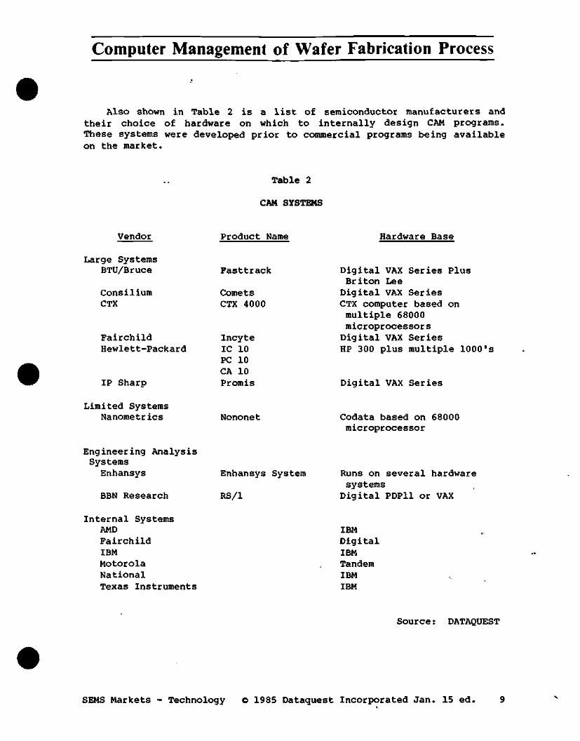
Computer Management of Wafer Fabrication Process
Also shown in Table 2 is a list of semiconductor manufacturers and their choice of hardware on which to internally design CAM programs. These systems were developed prior to commercial programs being available on the market.
Vendor
Large Systems BTU/Bruce
Consilium CTX
Fairchild Hewlett-Packard
IP Sharp
Limited Systems Nanometries
Engineering Analysis Systems Enhansys
BBN Research
Internal Systems AMD Fairchild IBM Motorola National Texas Instruments
Table 2
CAM SYSTEMS
Product Name
Fasttrack
Comets CTX 4000
Incyte IC 10 PC 10 CA 10 Promis
Nononet
Enhansys System
RS/1
Hardware Base
Digital VAX Series Plus Briton Lee Digital VAX Series CTX computer based on multiple 68000 microprocessors Digital VAX Series HP 300 plus multiple 1000's
Digital VAX Series
Codata based on 68000 microprocessor
Runs on several hardware systems Digital PDPll or VAX
IBM Digital IBM Tandem IBM IBM
Source: DATAQUEST
SEMS Markets - Technology © 1985 Dataquest Incorporated Jan. 15 ed.
Computer Management of Wafer Fabrication Process
CAM OPERATION STATUS
As of the beginning of 1984, merchant system suppliers have installed approximately 100 CAM systems in U.S. and European semiconductor manufacturing facilities. These installations are a mixture of systems that cover only fabs and ones that cover an entire manufacturing cycle. In addition to these systems, many of the larger merchant and captive manufacturers have developed and now use their own systems. The major applications for those systems already installed are WIP tracking, production reporting, feeding information to MIS systems, and data gathering.
Yield Improvement
Current developments in CAD systems will facilitate electrical yield improvement. These systems are used in yield analysis to correlate data coming from all of the manufacturing and test areas. By analyzing these data, process parameters can be changed to optimize yields. These analysis programs can be purchased independently from the tracking systems and can run on separate computers.
Production Scheduling
More efficient scheduling of material and time will help meet customer orders. With the recent rapid expansion of demand for semiconductors, lead times have stretched to months, and customer in-house inventories have been reduced to a level where meeting delivery dates of semiconductors is very important. A common situation in IC manufacturing is a fab with 100 products and 30 different product flows. Without computer scheduling of the fab floor and computer tracking of cumulative yield, it would be impossible to meet schedules or even know when a schedule was going to be missed. In the opinion of CAM system users, previous systems do not do an adequate job of scheduling this kind of situation. The schedule is even more difficult to control in assembly and test because of multiple package types and multiple electrical grades for each product.
Another use of the CAM system which is starting to be requested, is that of fab floor scheduling to maximize output. This type of capability is being requested for high-volume fabs running only a few products of one or two process flows. The emphasis in the CAM system changes from tracking WIP, to tracking and scheduling resources (equipment, labor, and indirect material). The mix can easily be controlled because it is not complicated by many products. With the mix under control, schedule objectives and customer needs can be met by increasing throughput.
10 © 1985 Dataquest Incorporated Jan. 15 ed. SEMS Markets - Technology

Computer Management of Wafer Fabrication Process
Learning Curve Improvements
CAM systems are also rapidly debugging new fabs and products, thus improving yields. If the CAM system is in place prior to a new fab being exercised, it brings all the data on its operation together. Therefore, when wafers are run, analysis can quickly be accomplished and corrective action taken. New products often need "tweeking" to improve yields or correct performance. With a complete manufacturing history available via the CAM system, decisions can quickly be made as to whether the problem is in the design or in the manufacturing process.
CAM Operating Limitations
Although significant gains can be made by implementing a CAM system, there are still problems to be overcome. The real-time control of both the process and data input are areas that are lagging in development.
Equipment Interfaces
Tracking process equipment performance and availability is very difficult if the equipment has not been interfaced to the CAM system; that is, if there is no communication link between the CAM computer and the microcomputer in the process equipment that controls and monitors it. The SECS protocol, established by SEMI in 1980, has allowed the implementation of this interface to proceed. However, so far only a few pieces of process equipment have developed such interfaces.
To operate within this limitation, some fab managers have improvised by using techniques such as "foot-net" or "sneaker-net." Using this technique, diskettes from processing equipment microcomputers, which contain records of process and equipment performance, are carried by an operator to the host and are placed in the CAM system disk controller. The information is then transferred under computer control to the CAM system hard disk. Obviously, this is not real-time tracking. Interfacing the equipment to the CAM system is the next step fab managers need to make in order to improve control of the operation. Both tracking of WIP and manufacturing equipment is needed for full automation.
Terminal I/O
The terminal is the standard communication link from the fab floor to the CAM computer. This communication method has its limitations. A typical IC fab sequence can have:
• 60 analytical measurement points
• 80 cleaning or stripping points
SEMS Markets - Technology © 1985 Dataquest Incorporated Jan. 15 ed. 11

Computer Management of Wafer Fabrication Process
• 150 process steps
• 200 transfer steps
Today, only about 20 to 30 of these points, or 5 percent, are logged into the terminal. The average logging and measurement results require 30 keystrokes per entry. The total keystrokes to log 30 points for a 2,500-wafer-start-per-week fab is 100,000 keystrokes per week. For a fab operator, a reasonable keying rate is 30 strokes per minute, or 3,300 minutes per week of logging time. This amounts to about 55 hours per week, or 1.5 operators. If all lot transfers and logging through process equipment were done on terminals, then 30 operators would be required. This is not reasonable, since this typical fab requires about 70 operators to process the wafers. To eliminate the need for additional operators, bar code readers, smart cards, or voice-actuated terminals must be added to complete the communication interface to the CAM system. This will be an interim solution for terminal I/O until the equipment can be interfaced to the computer through the SECS protocol.
CAM Future
CAM will eventually allow the full automation of semiconductor manufacturing. As discussed previously, there are significant hurdles to overcome. The following paragraphs discuss the evolution of manufacturing into full automation through the use of CAM systems.
Soft Automation
Semiconductor manufacturers are approaching the automation of fab operations very cautiously. It is premature for merchant suppliers to implement hard automation (i.e., automated WIP transport) in order to remain competitive. The greater risk appears to be trying to automate before equipment designed for automation is available and debugged.. As an interim step, semiconductor manufacturers are attempting to do complete "soft automation"; that is, real-time control and monitoring of equipment and WIP. (Real-time control is the control and monitoring of the equipment through a data link from the host computer.)
To accomplish this, the SECS protocol must be implemented on all process equipment and measurement instruments (i.e., V/I, film thickness, and line width). To do real-time logging of WIP without having excessive people in the fab, bar code readers must be added to equipment, and bar code labels must be attached to cassettes or cassette boxes. Terminals will still be needed (probably as part of the process equipment) to instruct the operators as to the schedule, lot processing sequence, and procedures. Real-time tracking allows much better control of schedules.
#
12 © 1985 Dataquest Incorporated Jan. 15 ed. SEMS Markets - Technology

Computer Management of Wafer Fabrication Process
Lots can be scheduled out of a fab on a. specific day rather than within a specified week, as is now the case.
Fab floor scheduling will be done by programs that optimize a particular result of the process sequence, such as:
• Maximizing wafer output of the fab
• Optimizing product mix schedules
• Meeting an out-schedule, but maintaining no greater than a certain amount of WIP
• Minimizing the effect of non-operative equipment by rescheduling other equipment workloads
These results require that the CAM programs have the ability to monitor equipment availability and WIP status from both after and before a particular process step. Decisions at a particular location can then be made, based on information about the whole process line.
Operators will play an increasingly passive role in the fab operation. Instead of telling the CAM system what material is at their work center, the CAM system will tell the operators to work on the material in a certain order. The operators will be told when a process sequence must be finished in order to maintain the schedule. The CAM system may also tell them to wait for lots that are expected to be there at a specified time.
Hard Automation
In order to implement hard automation, semiconductor manufacturers will need the following components:
A working system for real-time tracking and control
Highly reliable equipment
Automatic monitoring of equipment and process status by process equipment
Automatic transport of WIP
Staff of computer engineers
SEMS Markets - Technology © 1985 Dataquest Incorporated Jan. 15 ed. 13

Computer Management of Wafer Fabrication Process
By having a working tracking and control system, the smooth implementation of mechanical automation can occur; the communications link takes the place of manual entry at the workstations. This necessitates the existence of SECS protocol on the process equipment.
Part of a fully automatic system will require rescheduling and re-routing algorithms. These will resolve problems with routing when a piece of equipment malfunctions. Such equipment malfunctions must be kept to a minimum in order not to waste the capacity of other equipment. This will necessitate extensive preventive maintenance and equipment redundancy.
Equipment must have microprocessor control and monitoring of process and equipment status. There must be the capability for uploading and downloading data via the communications link.
The hard automation will include transport systems, robots, and buffer storage for cassettes. Two types of cassette transport systems are evolving—a "mail cart" type and a "track" type.
In the "mail cart" system, the cart, with several cassettes, moves between process equipment, guided by tape on the floor. The cassettes are carried in very clean, sealed chambers to achieve minimal particulate contamination on the wafers. This system is relatively flexible since process equipment location changes require only a re-routing of guiding tape on the floor to guide the cart to the new location. Veeco has developed a cart product, called the Veebot, and will market it in 1984.
In the "track" system, cassettes are transported in enclosed tunnels from one station to another. Such tunnels must be very clean to ensure minimal particulate contamination to the wafers during transport. This system is less flexible than the cart method, since changes in routing may necessitate mechanical changes to the track. However, the track system will run on simpler software programs than the cart system. Varian has introduced such a product, the Autotrack, and will ship the product in the last half of 1984.
Table 3 lists the automatic transport products that have been introduced. Some of the companies are still in the prototype stage of development. DATAQUEST estimates that it will take two years before a fab is built that can fully utilize auto-cassette transport systems.
Cassette buffering and robotized transfer will be required for either the cart or track approach. Cassette buffers must be used to increase equipment utilization by allowing temporary variation of local
14 ® 1985 Dataquest Incorporated Jan. 15 ed. SEMS Markets - Technology

Computer Management of Wafer Fabrication Process
throughputs. These occur during normal operation but are most severe when equipment malfunctions occur. Cassette buffers are also needed to store WIP during fab shutdown periods. These buffers will be located both locally, for material being processed, and centrally, to store cassettes waiting scheduling. Some form of robot will be required to transfer the cassettes from the transport system to the equipment.
Table 3
AUTCMIATIC TRANSPORT SYSTEMS
Company
Flexible Manufacturing Systems (FMS)
NACOM
Varian
Veeco Integrated Automation
Product
Computer-Integrated Manufacturing (CIM) System—cart type system
NAMTRACK—serial cassette transport
Autotrack—serial cassette transport
Veebot—series of carts and cassette buffers
Source: DATAQUEST
The popular conception of hard automation is the arrangement of equipment into "islands of automation," where pieces of equipment with complementary functions are grouped together. An example of this is integrating the lithography, photoresist, etch, and inspection processes into an in-line system. For small fabs, where equipment (or island) redundancy is not possible, the reliability of the equipment is of paramount importance in order to maintain the work flow. Even for larger fabs with equipment redundancy, the malfunction of one piece of equipment in an island will reduce the throughput of the fab. In these cases, MTTR (mean time to repair) and MTBF (mean time between failure) become important parameters for the balancing of line throughputs.
SEMS Markets - Technology © 1985 Dataquest Incorporated Jan. 15 ed. 15

Computer Management of Wafer Fabrication Process
Semiconductor manufacturers must be prepared to shift direct labor from an operator-oriented approach to an automated approach. This will require a significant investment in computer engineers. Even for a soft automation system, it is estimated that two years are required to receive maximum benefits from the system. Such benefits require personnel who know and understand the system. This underscores the fact that automated systems do not decrease direct labor costs, but simply transfer resource expenditures to more technically advanced areas.
CAM Research
Semiconductor companies are investing some of their research money in advanced manufacturing systems through the Semiconductor Research Cooperative. Thirty-two semiconductor manufacturers (merchant and captive) support this cooperative, which lets research contracts to universities for studies in semiconductor technologies. One-third of the research budget goes to the study of semiconductor manufacturing systems. These studies have two benefits:
• The supporting companies receive reports on the studies and can _ _ take part in the implementation of the new technologies.
• Universities are encouraged by the dissemination of money to do research in this field and to offer courses on manufacturing systems.
CAM IN JAPANESE FABRICATION
The character of Japanese semiconductor manufacturers has caused the CAM systems to be developed in a different way than in the United States. These influences are:
• Semiconductor manufacturing has developed within larger electronic and computer companies.
• The Japanese strive to keep WIP at low levels (just-in-time scheduling).
• Operators are not acquainted with keyboards.
• Non-employees are kept out of the fabs.
• The Japanese semiconductor industry has grown very fast.
16 © 1985 Dataquest Incorporated Jan. 15 ed. SEMS Markets - Technology

Computer Management of Wafer Fabrication Process
• There is little opportunity for small start-ups to service large companies.
• Japanese manufacturers use a large portion of U.S.-made equipment.
The result of these influences is that CAM systems have largely been developed in-house. Some of the more obvious characteristics of these systems are the use of bar code readers in place of terminals for logging material transfers, and the use of more complete communication links between processing equipment and computers. A U.S. company that is similar to the vertically integrated Japanese companies is Hewlett-Packard (HP). HP has also developed its own in-house WIP tracking system and early communication interfaces to process equipment. The HP Research Laboratory in Palo Alto was the main influence behind the establishment of the SEMI SECS interface.
DATAQUEST sees no indication that Japanese semiconductor companies are significantly ahead of U.S. companies in the use of hard automation (automatic transport of WIP) in fabrication. The higher electrical yields of the Japanese companies are probably due to better analysis of problems, better discipline of operators, increased drive for quality, and shorter throughput times.
CAM MARKET DATA
DATAQUEST estimates that total 1984 sales for CAM hardware and software systems for semiconductor fabrication in the United States and Europe will reach $40 million. We expect the size of this market to expand more rapidly than the overall rate of increase for semiconductor equipment sales. Many fab areas that are currently operating without adequate CAM support will purchase systems to install in their operating fabs. In addition, plant expansions and start-ups will implement CAM systems on an increasing percentage basis. As more users become educated on the use of CAM capabilities, the requirement for computing power and additional services will grow. Table 4 represents our estimate of U.S. and European sales of CAM systems.
Table 5 gives the sales history of companies supplying CAM systems for semiconductor manufacturing. All sales dollars are for combined hardware and software. Bruce, Consilium, and IP Sharp are third-party software houses and do not vend the hardware. To equalize these companies for actual semiconductor-related revenue, 50 percent of sales need to be subtracted. In 1984 sales are expected to increase 233 percent over 1983 due to the number of new fabs being constructed and the recognition by the user market that CAM systems are needed to run a fab of any significant size.
SEMS Markets - Technology © 1985 Dataquest Incorporated Jan. 15 ed. 17

Computer Management of Wafer Fabrication Process
Table 4
ESTIMATED U.S. AND EUROPEAN SALES OF CAM SYSTEMS (Millions of Dollars)
Sales
1983 1984 1985 1986 1987 1988
$13.0 $49.0 $60.0 $82.0 $115.0 $165.0
CAGE (1984-1988)
36.9%
Table 5
Company
Bruce
Consilium
CTX
Hewlett-Packard
I.P. Sharp
Total
CAM SYSTEMS SALES (Millions of Dollars)
1981 1982
$2.0
0.5
$4.0 4.0
2.0
1983
$ 1.0
4.0
1.0
5.0
2.0
1984
$ 2.0
18.0
4.0
15.0
10.0
$4.0 $8.5 $13.0 $49.0
Source: DATAQUEST
18 © 1985 Dataquest Incorporated Jan. 15 ed. SEMS Markets - Technology

Computer Management of Wafer Fabrication Process
Two companies not shown on Table 5 are Enhansys and BB&N, which specialize in analysis programs. These can be purchased as part of the system offered by the system suppliers shown on Table 5, or can be bought separately and run on off-the-shelf computers.
As the semiconductor industry shifts toward a commodity business, the main difference in semiconductor vendors will be the service that they provide to the customer. The semiconductor companies will all have the same resource availability and will have to deliver products at market-driven prices. DATAQUEST believes that a company's competitive advantage will come from efficient use of its manufacturing system. The CAM system is the glue that holds the system together and allows the user to direct and control the system's operation. The future leaders in the semiconductor industry will be those companies that are most skilled in the use of CAM systems.
SEMS Markets - Technology o 1985 Dataquest Incorporated Jan. 15 ed. 19

PACKAGING 11

Packaging
INTROPgCTION
This section discusses semiconductor packaging trends. The material covered in this section reviews the following;
• North American unit consumption data
• Packaging trends
• Packaging technology
• Packaging data
Various segments of this section are organized as follows:
• Bullet format for quick reading
• Tables and graphs designed for presentation format
Overview
Significant achievements in VLSI fabrication and design technologies have reached the point where concurrent improvements in packaging and die-level interconnection technologies are necessary for continued system performance. Of all the packaging and interconnection technology issues discussed, one issue readily agreed upon is that all users are going through a demanding transitional phase of component packaging decisions— decisions that will have to be dealt with in the near future, as the industry approaches submicron geometries.
The primary forces in the electronics industry driving the trends in component packaging are:
• Improved functional density (submicron geometries)
• Lower system/package cost
• Higher system performance
DATAQUEST believes that surface-mount devices (SMOs) will eventually offer the most cost-effective and viable of solutions to address the VLSI packaging dilemma in the consumer, commercial, industrial and military, and telecommunications end-user markets.
SEMS Markets & Technology £> 1986 Dataguest Incorporated May

Packaging
DATAQUEST expects that SMOs will continue to grow and emerge from today's insignificant small base to a major position in future years. While the traditional through-hole dual-in-line pacJcages (DIPs) will continue to grow in raarlcet share through the 1980s, we estimate that by the end of this decade, approximately 50 percent of all worldwide components, both passive and active, will be surface mount (either plastic or ceramic).
The package consumption estimates in Table 1 are based on DATAQUEST estimates of North American integrated circuit (IC) consumption. The figures reflect our estimates by major package format with allowances for yield losses.
Table 2 presents package use as a percent of total package consumption.
Table 3 shows the yearly growth rates by package type as a percent of total package consumption.
Table 1
B S T I M A T B O NORTH A M E R I C A N S H I P M E N T S B Y P A C K A G E T Y P E (Millions of Units)
Package 1982 1983 198* 1985 1984 1987 1988 1989 1990 CHSfi(8'i-90)
Plas t i c DIP 5,898 7,875 U,5'(8 CERDIP 920 l , m 1,562 Ceraitc DIP 66 80 107 Flatpack 35 37 *2 Ceraiic Chip Carrier 13 29 69 Plas t ic Chip Carrier/Ouad 7 19 57 Sa 4 13 40 PSA 2 4 9 Header 53 hh 84 Other 219 346 598
8,042 7,936 9,510 10,304 3,666 1,013
68 23 79 82 60 11 S3
492
930 62 18
127 164 127 17 47
574
1,038 68 17
250 402 329 33 52
812
1,047 67 14
443 891
820 51 9
611 1,531
767 1,390 59 81 51 38
1,039 1,032
7,403 652
40 6
855 2,672 2,560
114 30
1,041
- 7 . U -13.5X -15 .U -27.2X
52.111 89.7X
100.IX 52.IX
-15.9X 9.7X
Total 7,217 9,610 14,118 9,922 10,003 12,510 14,683 14,231 15,372 1.4X
Source : DATAQUEST March 1986
1986 D a t a q u e s t I n c o r p o r a t e d May SEMS M a r k e t s & Techno logy

Packaging
Table 2
ESTIMATED NORTH AMERICAN SHIPMENTS BY PACKAGE TYPE (Percent )
Packigt iVK 1983 1984 1985 1986 1987 1988 1989 1990
Plastic DIP CERDIP Ceraiic DIP FUtpack Ceraiic Chip Carrier Plastic Chip Carrier/Quad 30 PGA Header Other
81.7X 12.8 0.9 0.5 0.2' 0.1 0.1 .0 0.7 3.0
......
82.0X 11.9 0.8' 0.4 0.3 0.2. 0.1 .0. 0.7 3.6
81.8X 11.1 0.8 0.3-O.S 0.4 0.3 0.1 0.6' 4.2
......
81.IX 10.2 0.7 0.2 0.8 0.8 0.6 0.1 0.5 5.0 ....
79.3X 9.3. 0.6 0.2 1.3 1.6 1.3 0.2 0.5-5.7
. .
76.0X 8.3 0.5 0.1 2.0 3.2 2.6 0.3 0.4 6.5
...
70.2X 7.1 0.5 0.1. 3.0 6.1 5.2 0.4 0.3 7.1
-....«
60.9X 5.8 0.4 0.1 4.3 10.8 '.8 0.6 0.3 7.3
-,-,-,^^^
43.2X 4.2 0.3 .0 5.6 17.4 16.7 0.7 O.E 6.3
...
Total lOO.OX lOO.OX lOO.OX lOO.OX lOO.OX 100.OX 100.OX lOO.OX 100.OX
Table 3
S o u r c e : OATAQUBST Marcn 1986
ESTIMATED NORTH AMERICAN YEARLY GROWTH RATES BY PACKAGE TYPE (Percent )
Package 19B3 1984 1985 1986 1987 1988 1989 1990
Plastic DIP CERDIP Ceraiic DIP Platpack Ceraiic Chip Carrier Plastic Chip Carrier/Quad 30 PSA Header Other
33.5X 46.6X -30.4X -1.3X 19.3X 8.4X -15.9X 24.3 22.0 4.7
118.7 172.8 187.8 118.7 20.9 57.7
36. 34, 15.
140, 199. 216. 140.2
32. 73.
-35,2 -36, -45.
14.1 42, 50, 14,
-37,
-8.1 -9.8
-22, 61
101, 112, 61,
-10, -17.8 16.5
11.6 9.5
-6.0 96.3
144.8 158.3 96.3
8.5 41.5
0 -1
-15 77
121 133.5 77.5 -1.9 28.0
-21.7 -23.1 -34.0 37.8 71.B 31.3 37.8
-23.9 -0.7
-14.6X -20.5 -21.9 -33.
39. 74. 84. 39.
-22. 0.9
Total 33.1X 46.9X -29.7X 0.8X 25.IX 17.4X -3.IX 8.0X
Source : OATAQUEST Marcn 1986
SEMS M a r k e t s & Techno logy O 1986 D a t a q u e s t I n c o r p o r a t e d May
Packaging
PACKAGING TRENDS
OATAQUBST expects the following pacKaging trends:
By 1990f 50 percent of ICs used by OGMs will be surface mount.
Beyond 1990, tape automated bonding (TAB) will be the more viable interconnection and pacKaging technology.
Oual-in-line packages (OIPs) will continue to dominate mainstream IC pacKage applications.
Plastic OIPs will be the dominant packages through the 1980s.
DIPS will address the less than 48-pin package segment.
FlatpacK (a mature package technology) usage is declining. Prices will increase as volume declines.
DIP and flatpack will meet the 8- through 4d-lead package demands.
Use of CERDIPs will decline. CERDIP life cycle will be boosted by lower system cost hermetic applications.
Small-outline (SO) packages will be primarily used for small pin-count packages of 28 pins or less.
Chip carrier use will begin to grow in volume in 1986 and develop fully in the 1990s.
Leadless ceramic chip carriers (LCCCs) will address the more than 40 configurations.
Plastic Chip Carriers (PCCs) will address the 68-pin-or-less segment with 84-, 100-, and 124-lead versions under development.
Pin grid arrays (PGAs) will address the more than 84-pin VLSI segment.
TAB and flip-chip technologies for chip-on-board (COB) applications will grow significantly in the future.
1986 Dataquest Incorporated May SEMS Markets & Technology

Packaging
• Figure 1 shows OATAQUBST's estimates of paclcage consumption related
to the number of pins required by the circuit. The SO- and DIP-type paclcages will share the low-end segment. The chip-carrier and PGA pacKages are particularly suited to the 20-and-higher pin counts, with TAB clearly addressing lead counts beyond the 200 range.
Figures 2 and 3 illustrate changes in functional density over time. We believe that this trend away from the present level of functional density around 7 percent to the projected 42 percent in the 1990s is due to:
• The movement from conventional DIPs to SMDs
• Increased functional density
• Package pitch reductions
Figure 4 illustrates the potential opportunities for system cost reduction through the use of SMD package technologies. System cost is a function of size and materials. The lowest system cost can therefore be achieved via:
• The densest chip technology—VLSI
• Minimum chip encapsulation—SMT
• The lowest cost substrates—Plastic or epoxy glass
• Automated Assembly
Ultimately, we believe that cost reductions will be achieved by direct chip-on-board (COB) techniques. OATAQUBST expects COB techniques, already commonplace in the low-end consumer-oriented products, to mature sufficiently with the necessary quality and reliability to be used in other application areas.
SEMS Markets & Technology O 1986 Oataquest Incorporated May
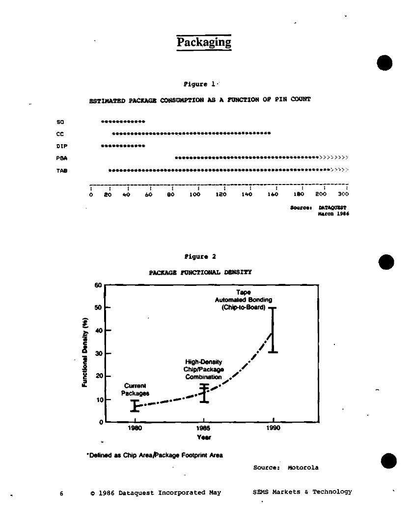
Packaging
F i g u r e 1•
ESTIMATED PACKAGE CONSOMPTION AS A FONCTION OF PIN COONT
SO
cc
D I P
PGA
TAB ^ > >>>':
ao <»o I
60 80 100 ISO 1<»0 160 180 eOO 300
Souccat MTAQOBST turcii 1986
e
2
60
50
40
30
I o 20
10
Figure 2
PACKAGE FUNCTIONAL DENSITY
Tape Automated Bonding
(Chip-to-Board)
Current Pacltages
High-Density Chip/Package . Combination , ^
X 1980 1985
Year
1990
'Defined as Chip AreaA*acl(age Footprint Area
Source: Motorola
1986 Dataquest Incorporated May SEMS Markets & Technology

Packaging
Figure 3
ACHIEVABLE BOARD DENSITIES BY PACKAGING TECHNOLOGY
300
200
u e
S a,
100
Tab
Advanced Chip Carrier
Chip Carrier
DIP
X 1985 1990
Year 1995
Source; OATAQUeST March 1986
SEMS Markets & Technology @ 1986 Dataquest Incorporated May

Packaging
Figure 4
COST-RBiXJCTION TRENDS
100
E S 50 CO
25
Standard DIP
Through-Hole
Board Assembly
Syetem Size
154 in / 62 in.* 62 in.'
31 in.'
Plastic-Leaded Chip Carrier and J-Lead Small-Outline Integrated Circuit Surface-
Mounted Components and Board Assembly
Two-Sided Surface-Mounted Board
Assembly
I 25 in.'
Tape-Automated Bonding or Flip-Chip
982 1983 1984 1984 + 1987 + Year
Relative Cost of Through-Hole, Surface Mount, and Bare Tab Systems.
Source : DATAQUEST March 1986
1986 D a t a q u e s t I n c o r p o r a t e d May SEMS M a r k e t s & T e c h n o l o g y
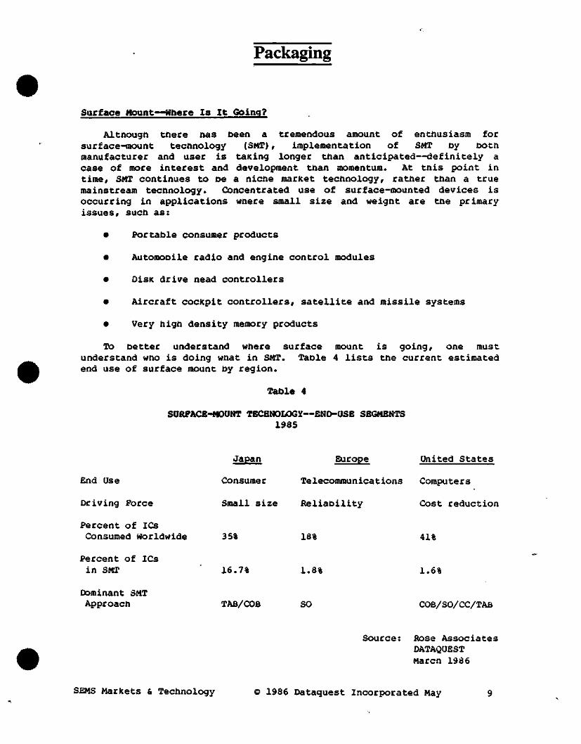
Packaging
Surface ttount—Where Is It Going?
Although there has been a tremendous amount of enthusiasm for surface-mount technology (SMT), implementation of SMT by both manufacturer and user is taKing longer than anticipated—definitely a case of more interest and development than momentum. At this point in time, SMT continues to be a niche market technology, rather than a true mainstream technology. Concentrated use of surface-mounted devices is occurring in applications wnere small size and weight are the primary issues, such as:
• Portable consumer products
• Automooile radio and engine control iiK dules
• OisK drive head controllers
• Aircraft cockpit controllers, satellite and missile systems
• Very high density memory products
To better understand where surface mount is going, one must understand who is doing what in SMT. Table 4 lists the current estimated end use of surface mount by region.
Table 4
SURFACE-MOUNT TECHNOLOGY—END-USE SEGMENTS 1985
End Use
Driving Force
Percent of ICs Consumed Worldwide
Japan Europe United States
Consumer Telecommunications Computers
Small size Reliability Cost reduction
35% 18% 41%
Percent of ICs in SMT 16.7% l . ( 1.6%
Dominant SMT Approach TAB/COB SO COB/SO/CC/TAB
Source: Rose Associates DATAQUEST March 1986
SEMS Markets & Technology O 1986 Dataguest Incorporated May

Packaging
The automobile Industry is the second largest user of SMOs in the United States. Oelco currently produces approximately 35,000 SMT boards per day for engine controllers and 15,000 print-and-etch boards per day for radio models.
Table 5 shows the percent of SMDs in specific consumer product areas in Japan in 1985 and their estimated use by 1990. The information is based on a survey conducted by the Japanese Printed Circuit Association.
Table 5
SURFACE-MOONTEO DEVICES IN JAPANESE CONSUMER PRODUCTS 1985-1990
Applications 1985 1990
Camera Electronic clock and watch Video camera Radio/radio cassette Sewing machine Stereo VTR Calculator** Television set 12.5% 31.9%
86.9%* 45.0% 40.1% 28.6%
0% 4.2% 8.8%
23.3%
94.3% 75.0% 69.9% 47.6% 42.5% 40.9% 36.2% 35.0%
^Percentages Number of SMDs Total number of components
**Nearly 99% of the functions are in one LSI
Source: JPCA DATAQUEST March 1986
10 © 1986 Dataquest Incorporated May SEMS Markets & Technology

Packaging
As shown in Table 6, National Semiconductor Corporation, Signetics, and Texas Instruments have introduced products in surface mount. However, the majority of other U.S. companies are not making the capital investment in surface-mount assembly lines and are relying more on the services of both onshore and offshore assembly companies. Highly automated assembly lines are being established in Hong Kong, Korea, Singapore, and Taiwan. It has been estimated that over the past five years, subcontract assembly has increased from 9 percent to 17 percent. Anam, the largest contract assembler in Korea, invested approximately $100 million in 1984 to upgrade its assembly facility to more than double its assembly capacity. Anam services approximately 48 U.S. semiconductor companies including Fairchild, Linear Technology, LSI Technology, Motorola, and SBBQ. Amkor/Anam is also planning an onshore facility in Pennsylvania for on-line production in 1986.
Table 6
SORFACE-NOUNT MANUFACTURING STATUS
Company Comments
National Semiconductor Corporation
All TTL, analog products available in surface mount; LS, ALS products in SO in less than 20 pins; PCC in 20 pins and more
5 percent of product types representing 30 percent of volume now surface mount
Tape-Pak—National's third-generation package; lead count feasibility to 284 leads/package on 0.020-inch centers
Signetics/ North American Philips
Plans to offer all TTL and analog products in surface mount
Using SO for 28 pins or less; PCC above 28 pins
Implementing TAfi over conventional wire bonded packages
Texas Instruments All bipolar logic, linear CMOS, and CMOS logic products available as surface mount
Offering SO integrated circuits, PCC, and single in-line package (SIP)
Source: DATAQUEST March 1986
SEMS Markets & Technology © 1986 Oataguest Incorporated May 11
Packaging
PACKAGING TECHMOLOGY
Major user concerns over choosing the most suitable package design include:
System application
Overall system cost
Manufacturer capabilities
Reliability considerations
Environmental constraints
Assembly techniques available
The selection process will continue to grow even more complex as new component and paclcaging technologies appear. For this reason, end users must maKe a concerted effort to analyze the advantages and disadvantages of VLSI device pacKages.
Through-the-Board
The printed circuit board with plated through-holes was developed in 1953 to replace the labor-intensive method of hand wiring electronic circuits. However, the through-the-board concept of mounting components on copper-etched phenolic or glass epoxy boards with predrilled holes was not implemented until the late 1960s.
The leads of ICs and discrete and passive components are inserted through the plated holes of the printed circuit board for soldering on the back side. The mounting holes and other holes for connecting the interconnect layers are gold plated to effect reliable contacts for easy solderability.
When all of the components are mounted, the printed circuit board is passed through a wave soldering process. During soldering, liquid solder flows across the bottom of the board and adheres to the leads and walls of the holes. This completes the electrical and mechanical connections.
12 © 1986 Dataquest Incorporated May SiiMS Markets & Technology

Packaging
Surface Mount
Small-outline (SO) pacicages and surface-mount techniques were developed in Burope for the Swiss watch industry in the late 1960s. SMT emerged in the United States in the mid-1960s in the form of surface-attached flatpacKs for use in missile-guidance computers. Japanese manufacturers adopted SMT in the early 1970s, as the need for miniaturization and cost reduction arose in consumer products such as watches and calculators.
Evolutionary changes in technology from LSI to VLSI and VHSIC devices are driving the transition from through-the-board insertion to surface mount. Table 7 lists the positive and negative attributes of SMT.
Table 8 shows the percent of cost and size reductions achieved using surface-mount technology to repacicage a printed wire board assembled in OIPs. Typically, the printed circuit board size can be reduced 30 to 70 percent when implementing SMT.
Reductions in plated through-holes and board layers also reduce or, in some cases, eliminate causes of failure, thus enhancing the reliability of a product. Table 9 is a comparison of DIP and PCC reliability test results performed at Texas Instruments' surface-mount research facility. Similar comparisons were made with SO and LCCC packaged components.
Another benefit of surface-mount devices is their ability to integrate with automated assembly technology, contributing further to improved reliability and cost reductions. Table 10 lists the estimated equipment costs for setting up a 5,000- to 30,000-square-foot surface-mount production line. Although the initial investment cost of equipment is high, reduced assembly costs are realized through less material, less space, ease of manufacture, and improved reliability. Eventually, surface-mount system cost will cross over through-hole cost via higher production volumes, capital equipment appreciation, and yield improvements.
SEMS Markets & Technology © 1986 Dataquest Incorporated May 13

Packaging
Table 7
ATTRIfiOTES OF SORFACB-MOUNT TECHNOLOGY
Positive
Features
Reduced Size & Weight
Cost
Surface-Mount
Packages 30 to 70 percent smaller; on botn sides of the board
Smaller boards
Lower component costs
Elimination of plated through-holes
Automated assembly
Less solder
Reliability
Increased Performance
Enhanced by having fewer interconnections
Shorter traces on substrate
Shorter device leads
Large variety of substrate materials (ceramic, plastic, porcelainized steel, mylar, glass, fiberglass)
Features
Cost
Reliability
Negative
Surface-Mount
Reduced cost offset by high equipment costs
Thermal stress resulting in cracKs on die and internal corrosion
Increased electrostatic discharge (ESD) problems due to handling and exposed parts
Flux removal with solder dip
Unseen copper slivers and burrs that occur during mechanical removal in solder dip
Source: DATAQUEST March 1986
14 o 1986 Oataquest Incorporated May SEMS Markets & Technology

Packaging
Table 8 .
ASSEMBLY TBCHNIQOE COMPARISON
Board Size
No. of Layers
Board Cost
Through-Hole
11" X 14" (154 sq. in.)
6
$150
Surface-Mount
6.5" X 9.6" (64 sq. in.)
4
$75
% Reduction
58%
33%
50%
Table 9
RELIABILITY OF A 64K ORAM DIP VERSUS PCC
Test Duration DIP PCC DIP PCC
Failure Rate Failure Rate FITS* FITS
OP Life 125° C 1,000 hours 0.14% T/flum 85° C/85% RH 1,000 hours 0.44% T/C -65° C/ISOO C 1,000 Cyc 0.51%
0, 0. 0.
.18%
.20%
.11%
70* 122
*Failures per billion hours **60% upper confidence limit at 55° C junction temperature Operating life: 1,000 hours at 125° C Temperature humidity: 85° C/85 % RH Temperature cycle: -65° C/+150° C
Source: Texas Instruments
SEMS Markets & Technology O 1986 Dataquest Incorporated May 15

Packaging
Table 10
ESTIMATED SORFACE-MOONT PRODUCTION LINE COSTS
Equipment Cost
Solder screener $ 60,000 PicK and place 200,000 Soldering system 90,000 Board cleaning 60,000 Visual inspection (automated) 120,000 fioard tester (manual) 100,000 Miscellaneous (repair, etc.) 100,000
Total $730,000
Source; Telctronix, Inc.
16 ® 1986 Dataquest Incorporated May SEMS Markets & Technology

Packaging
Table 11 lists available sources of piclt-and-place equipment, and test equipment used in surface-^nount technology.
Table 11
PICK-AND-PLACE/TEST EQUIPMENT SUPPLIERS
Piclc-and-Place
Amistar Corporation Celmacs Corporation Contact Systems Dynapert-Precima Engineered Automation Bxcellon Automation Fuji America Corporation Heller Industries, Inc. Ismeca USA Inc. Jergens, Inc. Mannix (Henry Mann, Inc.) MCT Circuit Assembly Division Nitto Kogyo Co., Ltd. Panasonic Industrial Co. North American Philips Co. Quad Systems Corporation Rohm Corporation Siemens Components Inc. Teledyne TAC TDK Corporation of America Universal Instruments Corporation Zevatech Inc.
Inspection/Test
Automation Unlimited, Inc. John Chatillon & Sons, Inc. Oognex Corporation ETP Everett/Charles, Inc. GenRad IRT Corporation Mannix(Henry Mann, Inc.) Photonic Automation Projectina Ltd. Teradyne UTI Instruments Company Vanzetti Systems Vichecic Zehntel Production Services
Source: OATAQUBST March 1986
SEMS Markets & Technology O 1986 Dataquest Incorporated May 17

Packaging
An alternative to capital equipment investment is the use o£ an assembly service that specializes in surface-mount technology. The key to using outside services is to maintain a close liaison with engineers during the design stage so that the correct component mix and assembly are chosen to arrive at the optimum benefits of SMT. The following is a list of companies located in the United States and specializing in SMT services and seminars:
Array Technology—Cupertino, California
ASMO, Inc.—San Diego, California
AWI—Santa Clara, California
Centralab—Milwaukee, Wisconsin
Integrated Networks, Inc.—Costa Mesa, California
Micro Industries—Westerville, Ohio
Nugraphix Group, Inc.—Los Gatos, California
SMT Technology Center/NA Philips—Milwaukee, Wisconsin
Solectron—San Jose, California
Reliability and Environmental Constraints
The main inhibiting factor for volume production of SMDs by large users (i.e., IBM, AT&T, Hewlett-Packard (HP), and Digital Equipment Corporation) is the lack of reliability studies on surface mount at this time. Hewlett-Packard's involvement in surface mount is basically in research and development, studying the physics and chemistry of surface-mount technology. HP's SMT activity is taking place mostly in the computer and medical divisions, where size and weight of SMT are a plus. Approximately 15 groups at HP are currently "looking" at SMT.
The largest contributors to ongoing reliability studies on surface-mount technology are National Semiconductor Corporation, North American Phillips Corporation/Signetics, and Texas Instruments.
18 © 1986 Dataquest Incorporated May SEMS Markets & Technology

Packaging
Thermal Management
One of the major considerations in package designs is the ability to cool the die or to conduct heat away from it. The heat generated from electronic devices affects not only the electrical characteristics of the circuits, but also the boards and substrates used. Temperature fluctuations cause both the boards and the material to expand and contract at different rates.
One solution to the thermal management problem that is employed by Texas Instruments and other manufacturers is to use a printed circuit board material with the same thermal coefficient of expansion (TCE) as the component. Table 12 lists the advantages and disadvantages of specific board materials in current paclcage development.
Table 12
PRINTEO WIRING BOARD MATERIAL
i M r t Mauhal
Eooiy Fibergiau
Poiymioe Kariv
Polymae QuvQ
Alumina iCtmiic)
Coooer-invar-Copper
ComDiiani Layer Sufisiran
Esoxy KcvW
Comoosite Meai Foil MLB'S
TCClPfmrC)
12-16
4^
6-«
6.S
64
NOUI
6-8
Note 2
MnnlitM SuOstraK sio. imgptL most common M I U M Soard material, conventionat PWB ofocessing
SuMiate sin. oeiqnt lesairaOilKy: uses conyemional PWB siocessing and matsies TCE ol ceramic
Sia. meignt, reoaiiafiiiiiy. good uieiectnc oiaoerties. conyemional PW8 groctssing tecnnioues. CTS matcti
Ejiadty maicnes TCE ol ceramic cnip canien good heat itwrmai conductivity
TCE ol ceramic, excellent itiemai conductiyityi mneieni ground Diane. EMI/RFI sdieiding
Suostiata si2e. reoairaoiiityi good dieiectnc oiQoerties. TCE itaicn to ceramic mrougn ceramic miougri compnaiit layer
Suostrate sue. meigm. repairaoiiiry. STE matcn. conventional PW8 oracessing lecnmoues
SuOsiiate size, reoairabiiity uses conventional M U processing tecnmques. oravides good TCE matcn
OleaimittgM
Poor inetmal conouctiviiy TCE provides good inaicl) to Tl's PIXC Put poor tor ceramic
OiHicult to macnine. nign cost, resin mictocracKing and Mier adsorption
Oilficuit to drill vias. avaiiaDiiiiy
Meignt. cost fragility reguires mia-iilm screening piocessing. limited suPstrate sis
Some meignt increase, requires mioi-tilm screening piocessing
Poor mennai conduaiviiy smi 'n devdopment stage
Resin micraciaaung 4ter temo cyae and mater adsorption
Avaiiaole amy tor MLS's. not commonly avanaoie
Notes: 1 Compliant layer cpntomn to TCE ol me ceramic cnip carrier and tn Base PWB matenai 2 SuDstitutes cppoer-ciad invar loii tor PWN and QNO planes used in muiti-iayer Poards. The copper-clad invar supplies TCE compliancy
Source: Texas Instruments
SEMS Markets & Technology O 1986 Dataquest Incorporated May 19

Packaging
Directions in Cooling and Heat Removal
As LSI devices become more complex, they tend to dissipate more power. If tnis power is not dissipated by the paclcage, the temperature of the semiconductor die can increase to the point where performance or reliability can be degraded. Power densities have steadily increased, reaching 8 to 10 times the 1970 levels in low-end systems. Oesign-based system-level solutions being implemented to improve power-handling capabilities include:
• Cooling techniques
Providing direct thermal as well as electrical paths at system interfaces, as junction design and materials choices will minimize thermal resistances
Placement of heat-generating devices on the board in contact with bracKets or other paths to the environment
Designing board spacing and placement with air flow in mind
• Heat removal techniques at the board level
Constructing the board with cooling pipes through which conductive/convective cooling may be accomplished
Use of copper core or hollow core to increase the surface of heat transfer
• Heat removal techniques at the pacKage level
Using mold heat-conductive inserts in the body of a plastic paclcage
Affixing heat sinlcs to paclcages for high-power devices
• Heat removal techniques using specific materials at the board and package levels
Incorporating thermally conductive fillers into epoxy glass to increase conductivity
Supplementing glass fibers with inert fillers to decrease the board's thermal coefficient of expansion
20 © 1986 Dataquest Incorporated May SEMS Markets & Technology

Packaging
-* Building thermal "bridges" between the device and the board with thermally conductive glue
r- Developing copper alloy lead frame materials with increased conductivity
Texas Instruments has accomplished a strategic substrate development using multilayers of copper-Invar-copper. As shown in Figure 5, the material is a sandwich of an Invar core between two layers of copper. Texas Instruments has found that the low TCE of the core dominates the TCE of the overall board for a reliable mount of a leadless ceramic chip carrier. -
Figure 5
COPPER-CIAO INVAR MULTILAXER BOARD
' /y Jy . // / .'/////^l^nK
/ J ..- . ^ / / J / / / // / T-TT
' ( • ' i " y { ' \ ^ ' ^•\>>,f^^'^'"''''>>^'''-\ • • * ^ M fc • •• • •• r r - r N ^ a J J . f r, i r, • i , i •^ r r> • i ^ i ^ J i
\\X\\\\~ \x\\\'- -\'-
u > r . ' . •> •' ^ •• y / / , ' . ' / /
• ' ' - ' • • - - ^ - • •
• 0014 COPPEB lSlG^^ALl
• a w EPOXY-GLASS
• 0014 COPPER (SIGNAL)
• 006 EPOXY-GUVSS
• 005 COPPER CLAD iNVAR GRCUNOl
• 0O4 EPOXY-GLASS
• 0O5 COPPER CLAD iNVAH i POWER)
• '0O6 EPOXY-GLASS
•Q014 COPPER I SIGNAL)
• •M4 EPOXY-GLASS
• M14 COPPER :SlGNALi
DIMENSIONS IN INCHES
Source: Texas Instruments
SEMS Markets & Technology O 1986 Dataquest Incorporated May 21

Packaging
National Semiconductor Corporation is currently using perforated lead frames in their small-outline (SO) packages to prevent contamination on the inside of the package and the formation of cracks on the die. Use of the perforated lead frames allows a continuous path for molten compound, thus improving the reliability of the product. National uses a lead frame with a high-copper-content alloy rather than alloy-42f as copper alloy leads have better thermal dissipation and thermal expansion and cost less than alloy-42.
Surface-Mount Assembly
Surface mounting is a process whereby a packaged IC or other component is designed to be physically mounted on the surface of a printed circuit board (PCB) instead of inserted into holes through the PCS. Surface-mount package technologies for active components consist of small-outline, chip-carrier (plastic and ceramic), and tape automated bonding. Passive components, chip resistors, and chip capacitors are also available in surface-mount packages.
During the surface-mount assembly process, as shown on Figure 6 interconnect traces are screen printed onto the surface of the PCB. Screen printing is a widely used method for applying solder paste to the PCB. After applying the solder paste to the board, the components are placed on the board manually or with automated pick-and-place equipment. Some types of pick-and-place equipment apply glue to the component before placing it on the board. The board is then cured to set the solder paste and adhesive. Solder paste is preferable to glue as the primary adhesive because the component tends to self-align as the solder melts during the reflow process, matching leads to the traces. The board and its components can either be baked at 50 to 80^ C for 45 minutes or allowed to stand at room temperature for approximately 12 hours. If devices are required on the bottom side of the board, the board may be inverted at this point and the process repeated on the other side. The board is then run through a reflow soldering system. After reflow, the board is cleaned to remove the flux (metal binding medium used in soldering) residues and is visually and electrically inspected.
22 ® 1986 Dataquest Incorporated May SEMS Markets & Technology
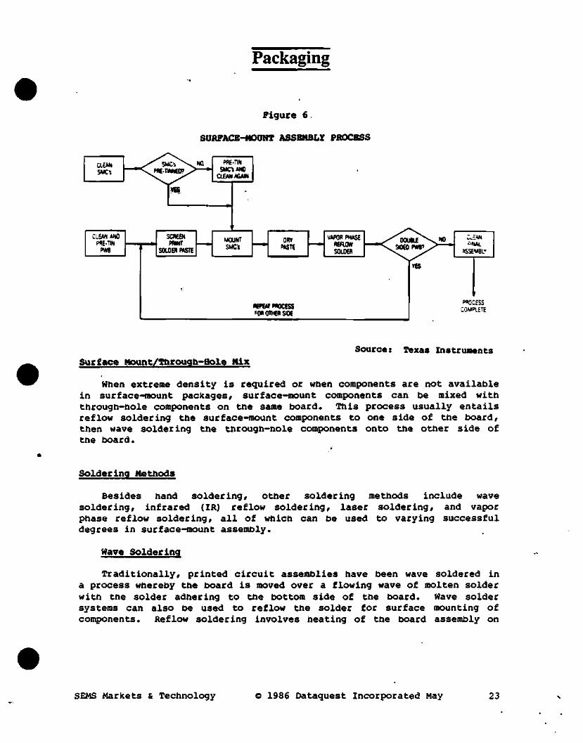
Packaging
Figure 6.
SOAFACB-MOONT ASSEMBLY PROCBSS
CLEAN SMCi
CLEAN M*0 PflE-TIN
(>W8
SCREBl PfflNT
SOLDER PASTC
UOUMT SMC^
out f»STE
VAPOR PHASE REFUM SOlOER
REPEAT PROCESS FDR OTHER SIDE
Source: Texas Instruments Surface Mount/Througfa-Hole Mix
When extreme density is required or when components are not available in surface-mount paclcages/ surface-mount components can be mixed with through-hole components on the same board. This process usually entails refiow soldering the surface-mount components to one side of the board/ then wave soldering the through-hole components onto the other side of the board.
Soldering Methods
Besides hand soldering, other soldering methods include wave soldering, infrared (IR) refiow soldering, laser soldering, and vapor phase refiow soldering, all of which can be used to varying successful degrees in surface-mount assembly.
Wave Soldering
Traditionally, printed circuit assemblies have been wave soldered in a process whereby the board is moved over a flowing wave of molten solder with the solder adhering to the bottom side of the board. Wave solder systems can also be used to refiow the solder for surface mounting of components. Refiow soldering involves heating of the board assembly on
SEMS Markets & Technology O 1986 Oataquest Incorporated May 23

Packaging
which solder paste has been screened onto the PCB metal pads. The board is heated until the paste melts and flows around the leads and pads. Many manufacturers currently assemble both sur£ace-!-mounted components and through-the-board components on one board (see Figure 7) because many products are not available in surface mount. Various surface-mount and lead-insertion methods include all on top, all on bottom, or some on top and some on bottom.
Figure 7
NAVE SOLOBRING A MIXTURE OF OIPs AND SNDs
PC BOAflO
Olf . WSfSTDBS ANO/M CA«Ciro«S
Source: Texas Instruments
Infrared Reflow Soldering
Infrared reflow soldering involves absorption of radiant energy to neat the assembly and materials. The assembly board passes through a preheated zone that slowly heats the solder paste. After preheating, the assembly enters the next heating zone, where increased temperatures result in reflow. The assembly is then cooled. Infrared reflow solder equipment is available from the following suppliers:
fi Argus International—Hopewell, New Jersey
• Oynatherm—Santa Clara, California
24 1986 Oataquest Incorporated May SEMS Markets & Technology

Packaging
•
• Electrovert—St. Louis, Missouri
• Intex—Broo<efield, Connecticut
• Mannix (Div. of Henry Mann Inc.)—Huntingdon Valley, Pennsylvania
• Radiant Technology Corporation—Cerritos, California
• SiKama International—Santa Barbara, California
• Vitronics Corporation—Newburyport, Massachusetts
Laser Soldering
Laser soldering involves applying a rapid pulse-liKe heat for a short duration to individual solder joints but not to the component. The infrared heat is radiated from either a carbon dioxide (CO^) or solid-state Neodymium-doped Yitrium-Aluminum-Garnet (Nd:YAG) YAG laser. While a more precise and reliable solder joint can be achieved through laser soldering, its primary disadvantage is speed and therefore is considered a specialized soldering technique. This soldering process is used for dense packaging and is an ideal process for attaching heat-sensitive components. Laser soldering is used in niche paclcaging application areas such as military and ceramic hybrids. Laser soldering systems are available from the following suppliers:
• Apollo Laser—Los Angeles, California
• Coherent General—Sturbridge, Massachusetts
• US Laser—WaldwicK, New Jersey
• XMR—Santa Clara, California
• Lumonics, Inc.—Tempe, Arizona
Vapor Phase Reflow Soldering
The vapor phase reflow soldering method was developed by Bell Laboratories. Basically, a component assembly is immersed in a layer of vaporized inert fluorocarbon. The fluid boils at .215° C, which is exactly the correct temperature for solder reflow. The vaporized fluid condenses on tne assembly and surfaces that it contacts, heating all surfaces uniformly and causing the solder paste to reflow. Figures 8 and 9 illustrate the single-layer in-line and two-layer batch vapor systems.
SEMS Markets & Technology © 1986 Dataquest Incorporated May 25

Packaging
Figure 8
IN-LINE SINGLE VAPOR PHASE SYSTEM
HCAnNGBiMCNTS
STAIMiSS STEE TANK
Sourcat T«xaa InstruiMnts
Figure 9
BATCH-TYPE VAPOR PHASE SYSTEM
ASSEMBLED PWB
SOLOEPEO ='JV8
/
SECONOAflY VAPOR UYER FREON' TF
•
PRIMARY VAPOR LAYER INERT FLUOROCARBON
AT 215*C
SOILING LIQUID FLUOROCARSON
1
f 1
t r~
_=_] •HEATING ELEMENT
3 " I I N L £ S S S*EEL 'Am
Source: Texas Instruments
26 © 1986 Dataquest Incorporated May SEMS Markets & Technology

Packaging
Vapor phase equipment suppliers include:
Baron-Blakeslee—Melrose eacK, Illinois
Centech Corporation—Minneapolis, Minnesota
Corpane Industries, Inc.—Louisville, Kentucky
Hollis Engineering—Nashua, New Hampshire
HTC—Concord, Massachusetts
Lenape Equipment Co.—Lakewood, New Jersey
Mannix (Div. of Henry Mann, Inc.)—Huntingdon Valley, Pennsylvania
Multicore~Westbury, New Xoric
Lead Frames
Lead frames are the basic pacKage assembly for plastic and CERDIP packages. Production quantities of lead frames are fabricated by stamping. Stamps are precision cutting tools that, litce cooKie cutters, extract the desired patterns from sheets of metal. Stamping produces lead frames at low unit costs after the expensive cutting tool has been amortized. Therefore, it is a good process for high-quantity production. Low-quantity production typically uses etched lead frames to eliminate the tool costs and lead times required for stamped frames. Table 13 lists the manufacturers of lead frames.
SEMS Markets & Technology © 1986 Dataquest Incorporated May 27

Packaging
Table 13
LEAD FRAME SUPPLIERS
Company
Advalloy/ Inc. Advanced Semiconductor Materials Int. Inc. Caribidex Composite Technical Alloys, Inc. Oage Limited Dyna-Craft, Inc. W.C. Heraeus QmbH Interconics (BMC) Interconsal Assoc. Inc. International Leadframe Corp. Kras Corporation Meco Metal Finishing Engineers BV Oberg Industries, Inc. Oriental Chemical Ind. Pan Metal Corp. ShinKo Electric America, Inc. Stamping Technology Sumitomo Metal Mining Texas Instruments Wadsworth/Bryant Worlteic Inter., Ltd. Youngwood Metals
Location Stamped Etched
Palo Alto, California X X
Phoenix, Arizona X X Southgate, Michigan X
Attelboro, Massachusetts X X Great Britain X X Santa Clara, California X X West Germany X x St. Paul, Minnesota X x Palo Alto, California X x
Santa Clara, California X x Fairless Hills, Pennsylvania X X
The Netherlands X X Freeport, Pennsylvania X Seoul, Korea X X Los Angeles, California X X
Santa Clara, California X X Milpitas, California X Fremont, California X X Attelboro, Massachusetts X Menlo Parle, California X X San Mateo, California X . X Murraysville, Pennsylvania X
Source: DATAQUEST March 1986
Ceramic Paclcage Suppliers
As previously discussed, ceramic pacKages include ceramic DIP, ceramic flatpacK, ceramic chip carriers, and pin grid array packages. Table 14 lists the available suppliers of ceramic packages.
28 © 1986 Dataquest Incorporated May SEMS Markets & Technology

Packaging
Table 14
CBflAMIC PACKAGE SUPPLIERS
Company
AMP, Inc. ASP£, Inc. AVX Ceramics Corporation Airpax Corporation Augat, Inc. Barry & Associates Bourns, Inc. Brusn Hellman, Inc. Burndy, Inc. CTS Corporation Ceradyne, Inc. Circuit Assemialy Corporation Coors/Ceramics Dage Limited Oande Plastics, Inc. Demetron, Inc. Oiacon, Inc. £merson & Cuming, Inc. GE Ceramics, Inc. Gibson-Egan Co. W.G. Heraeus QnbH Hestia Tecbnologies Hoechst Ceramtec NA Inc. Hoecbst Informations-TectiniK Interamics Kras Corporation Kyocera International, Inc. M/A-COM Semiconductor Products Microelectronic Paclcaging, Inc. NTK Tecnnical Ceramics Naramics National Beryllia Corporation Rosentnal Tecnnilc NA, Inc. SninKo Electric America, Inc. Spec Industries, Inc. Textool Products Vichem Corporation Wells Electronics, Inc.
Location
Barrisburg, Pennsylvania Fairchild, New Jersey Myrtle Beach, South Carolina Cambridge, Maryland Attelboro, Massachusetts Los Altos, California Riverside, California Cleveland, Ohio NorwalK, Gonnec t icu t Ellchart, Indiana Santa Ana, California Irvine, California Golden, Colorado Great Britain Somerville, New Jersey Union City, California San Oiego, California Billerica, Massachusetts Chattanooga, Tennessee Ouarte, California West Germany Santa Clara, California Providence, Rhode Island West Germany San Oiego, California Fairless Hills, Pennsylvania San Diego, California Burlington, Massachusetts Scottsdale, Arizona Nagoya, Japan Nagoya, Japan Haslcall, New Jersey Providence, Rhode Island Santa Clara, California San Marcos, California Irving, Texas Stanford, California South Bend, Indiana
Source: DATAQQEST March 1986
SEMS Markets & Technology & 1986 Dataquest IncorE>orated May 29

Packaging
Soclcets
Integrated circuits in high-lead-count packages are expensive and difficult to remove from soldered boards. SocKets allow integrated circuits to be readily removed or replaced during assembly and test or retest; they also help to isolate particular functions and to diagnose problems.
SocKets are frequently used with standard JBOCC (Joint Electronic Devices Engineering Council) and non-JBOEC chip-carrier paclcages because socKets reduce the problem of stress due to thermal expansion. The glass epoxy circuit boards that are commonly used in commercial systems expand with heat at a different rate than does the ceramic material in the chip carrier. The open-frame construction of the soclcet permits maximum air flow, allowing even heat dissipation on all sides. The flexible leads, lids, and latches of the socKet ensure uniform electrical contact and absorb the expansion while eliminating or reducing rejections due to breakage or marring. Soclcets have been designed for burn-in applications at up to 200° C.
PACKAGE DATA
Dual-In-Line Packages
The dual-in-line paclcages (OIPs) employing both plastic and ceramic technologies currently account for more than 85 percent of the IC pacKage consumption in North America. The standard DIP introduced in the 1960s has dominated IC paclcage applications, growing with LSI developments from 14 leads up to 64 leads. The DIP derives its name from its two rows of in-line leads. The dual-in-line paclcage is performance limited by its 0.100 pitch or lead spacing. Thus, while pin counts up to about 64 can be handled by dual-in-line packaging, the size, weight, and electrical performance characteristics of the DIP are better suited to the less than 48-pin count. The demands for density have promoted development of new DIPS. The shrink DIP uses either 0.079-inch or 0.050-inch centers for the pins. Hitachi has introduced its digital components in a shrink DIP package with 1.778mm lead pitch, the skinny DIP with a 2.54mm lead pitch, and the zig-zag-in-line package (ZIP) which has two rows with a 2.54mm lead pitch. DATAQUEST estimates that approximately 3 percent of the 256K DRAMS manufactured worldwide are currently packaged in ZIPs. Beyond 48 leads, an insertion-mount type of package, such as PGA, LCCC, flatpack, or quad-in-line package (QUIP) becomes more feasible.
Figure 10 illustrates the various types of DIPs available.
30 © 1986 Dataquest Incorporated May SEMS Markets & Technology

Packaging
Figure 10
0(JAL-IN-LINB PACKAGE TYPES
Plastic Ceramic
Encapsulated Co-fired Premolded CEROIP
Ceramic glass
Source: DATAQUEST March 1986
The ceramic OIPs incorporate a multilayer ceramic body featuring brazed-on leads and a die-mounting cavity that has a solder-sealed metal lid. The major sealing technique uses a gold-plated metal lid and a gold-tin eutectic sealing preform. A more cost-effective ceramic DIP is one incorporating a glass seal to attach the lid to the pacltage. MOS PROMs, which can be erased with ultraviolet light, are sealed with a transparent quartz lid. Ceramic DIPs consist of top-brazed, bottom-brazed, and side-brazed pacKages.
CEROIP paclcages consist of two ceramic body parts and a lead frame. After the IC chip is attached and wire bonded to the lead frame, the pieces are run through a furnace and fused with a glass seal. CEROIPs are typically available in the DIP configuration witn available pin counts of 8, 14, 16, 22, 24, 28, or 40 pins. Improvements in plastic molding compounds and increased popularity and demand for chip carriers and SO packages will displace CEROIPs as standard pacKages.
CEROIP pacKages offer the least-expensive hermetic technology available. Historically, the majority of CEROIP packages have been used in military applications because they meet both military package specifications and overall mechanical requirements for a hermetically sealable package. CEROIPs will continue to be the Key package for military end-use applications through the end of the decade. However, critical light weight and size issues along with improvements in hermetic construction and package reliability will drive chip carrier and TAB usage by the military market. For ground-based systems applications with heavy cooling and thermal demands, pin grid arrays have been shown viable for use in military programs. Major improvements in packaging methods used in military programs have been made by the VHSIC program contractors. Package types developed for VHSIC chips are pin/pad arrays and chip carriers.
SEMS Markets & Technology © 1986 Oataquest Incorporated May 31

Packaging
When the C£ROIP package was first developed, it was not considered suitable for MOS applications because contaminants released from the glass during sealing could cause degradation of the MOS die. Improvements in die-attach materials and sealing techniques have now largely eliminated this problem. In 1983, Intel Corporation developed a silver-loaded glass system, as a nongold die attach substitute in CEROIP packages. The silver/glass system offered significant cost and processing advantages for use in CERDIP packages. A CEROIP package with a bull's-eye lid used in HOS EPROM and BEPROM applications incorporates a glass lid that will transmit the ultraviolet light used for erasing the PROMs. Fujitsu recently introduced its 512K CMOS EPROM in a CEROIP package, and Xicor introduced its 256K EEPROM in a 28-pin CEROIP package.
Plastic encapsulated OIPs are assembled using a transfer molding technique incorporating epoxy materials and lead frames. The IC chip is attached and wire bonded to the lead frame. Sealing is effected by encapsulating the IC and lead frame in injection-molded epoxy. Traditionally, plastic ICs have been bonded with gold wires. More recently, manufacturers have implemented silver plating on the package instead of gold.
As plastic is a poor thermal conductor, manufacturers are using copper lead frames to enhance power-handling capabilities. While the plastic package is not hermetic, it does offer a low-cost alternative to ceramics.
Flatpacks
The standard flatpack configurations have center-to-center 50-mil lead spacing. Flatpacks are essentially flat rectangular packages with bodies constructed of either alumina or beryllia. Early flatpacks were designed with glass-to-metal seals. Traditionally, flatpacks have not been considered a mainstream industry-standard package. Flatpacks have been used significantly in military applications to satisfy dense packaging requirements. Flatpacks are surface mounted; because of their structure, they are difficult to automate. Flatpacks are also frequently welded to the printed circuit board, making them susceptible to lead damage in handling.
Chip Carriers
The chip carrier is a four-sided package with leads on all four sides of the carrier, usually arranged on 0.050-inch center-line spacings. Chip carrier configurations are available in 44, 52, 68, 84, 96, and recently as many as 300 leads. Chip carriers may be leaded or leadless
32 © 1986 Dataquest Incorporated May SEMS Markets & Technology

Packaging
and may oe made of ceramic or plastic. They are surface-mounted pacicages designed for mounting to a substrater for socket insertion, and for through-hole mounting applications. Figure 11 shows the JBOBC chip carrier types and specifies some of their construction characteristics and mounting criteria. The JBOEC-labeled chip carriers are types A, B, C, and D and are leaded or leadless packages. OATAQUBST expects that tne ceramic chip carriers will become the major packages for military and specific telecommunications applicationsr while the leaded plastic and leaded ceramic chip carriers will be the dominant carrier packages in all other applications. The advantages of chip carrier packages include:
• Size and weight
- Volume—Potentially a 16:1 reduction over the DIP
- Weight—Potentially a 12:1 reduction over the DIP
System PCB count 8:1 reduction over the DIP
• Reliability and rework
Low mass of chip carriers improves mechanical shock and vibration resistance.
Increased density allows reduction in plated through-holes.
• Parametric
- Resistance and capacitance reduced by 55 percent
• Improvements
- Average inductance reduced by 90 percent
- PCB resistance
- Improved switching times
• Potential cost reductions
• Automated assembly
~ Smaller assembly line
- Yield improvement
» Basy rework
SEMS Markets & Technology © 1986 Dataquest Incorporated May 33

Packaging
F i g u r e 11
JEDBC-RBCOGNIZBO CHIP CARRIER TYPES
MS006 MS002 MS003 MS004 MS005 MS007 MSOOe N/A
Metal C«nmic S«aling Cov»r
R*c«3S«d Mstai
Caramic Ssaling CoMr Lid
Handling labs Epoxy Drop
Laadiass Laadiess Type A Type 8
Leadiess TypeC
Laadless TypeD Minl-Rak
Edge Conductors In Grooves
Solder
Source: 3M Company Leadless Cergunic Chip Carrier
The leadless ceramic chip carrier (LCCC) is a symmetrical pactcage with metallized leads extending from the die-attach cavity to the periphery of the substrate, down the edges, and slightly around the underside. Users should be aware of these three main obstacles to mounting LCCCs:
^ Thermal management of the assembly to handle the increased pacKing density
A Solder-joint fatigue and failure due to the thermal coefficient of expansion (TCE) difference between the chip carrier and the printed circuit board
• Solder-joint failure due to flexing, warping, and twisting during processing, system assembly, and operation
The Metallurgical Materials Division of Texas Instruments has developed a multilayer epoxy glass board with copper-Invar-copper substrates to hold the solder-mounted chip carriers. Company packaging managers have concluded that the advantages of this copper-clad metal system include rigidity, improved dimensional stability, inherent heat sinning, TCE matching, integral ground and/or power plane, EMI/RFI shielding, and large area availability. Figure 12 is an illustration of how vias are used to conduct heat from high-power components to the core for improved thermal control.
34 1986 Dataquest Incorporated May SEMS Markets & Technology

Packaging
Figure 12
THROaGH CONOOCTIVITY OSING VIAS
IC CHIP 80N0ING f>«l
SOLOW FILLET iWHESS CERAMIC CHIP CAftfliER
ELECTBlCAlVl* m s CROSS-SECTION
Source: Texas Instruments
Leaded Ceccunic Chip Carriers
The leaded chip carriers, also referred to as Type C by JEDBC, include the Quad Surface Mount, the Plastic Chip Carrier (PCC), and the Leaded Chip Carrier (LCC). The "J" leads of the leaded ceramic chip carrier allow it to be used with epoxy circuit boards, without installing socKets. The most common assembly method is to attach clips to the metallized carrier edges. The clips can be seen in Figure 13. Depending on the choice of bend, the carrier can be mounted to the circuit board with either surface mounting or through-hole mounting techniques. The LCC offers the handling and board mounting advantages of the PCC with the reliability characteristics of ceramic for military applications.
SEMS Markets & Technology © 1986 Dataquest Incorporated May 35

Packaging
Figure 13
LEADED CERAMIC CHIP CARRIEA
Source: OATAQUEST Marcb 1986
PCCs are primarily intended for surface-mount applications. Figure 14 illustrates the lead configurations for the PCC. Hie "J" form or rolled-under configuration is the JEOEC preferred version, since it displays the same footprint as the LCCC and takes up the smallest amount of board space. The problem of TCB differential between the printed circuit board and the device does not occur because the leads are designed to absorb thermally induced stress.
36 1986 Dataquest Incorporated May SEMS Markets & Technology

Packaging
Figure 14
PCC LEAD CONFIGURATIONS
JJMMJ JUWA. SiPi
ROIXEIMINOCR
OULL-WWiO
BUTT-LEAO
PLAT LEAD
Source: National Semiconductor Corporation
Small-Outline Integrated Circuits (SOICs)
The small-outline (SO) pacKage is basically a DIP configuration with leads on 0.050-inch centers. As shown in Figure 15, its leads are bent down and out from the body of the pacKage for surface mounting. The SO occupies approximately one-fourth of the circuit board area required by the DIP, and it has the lowest profile of any of the pacHages in use. Its construction is essentially identical to that of the plastic DIP. Because it uses the same lead frame material and thicKness as the plastic DIP and has very short leads, it is extremely rugged. Companies are developing wider-bodied (above 155 mils) packages in 18-, 20- and 28-pin counts.
Figure 15
SMALL-OUTLINE VERSUS PLASTIC DIP
-^f^^^^^
SO Outline Plastic Dip
Source: Signetics Corporation
SEMS Markets & Technology © 1986 Dataquest Incorporated May 37

Packaging
The SO pacKage is popular in the hybrid industry because it facilitates testing and handling while offering small size. It is experiencing significant demand from the electronic camera, automotive, and telecommunications industries. It is especially popular for the pacKaging of analog ICs.
Pin Grid Arrays
The pin grid array (PGA) shown in Figure 16 is square in shape, with an array of pin locations on the underside of the pacKage for through-board or socKet mounting. The grid has a 0.100-inch row spacing. The PGA is available in cavity-up or cavity-down versions. The cavity-up version, as shown, eliminates the pins from the center of the substrate to maKe room for the die-attachment cavity. This cavity orientation places the die substrate in contact with the upper surface of the pacKage and with any heat sinks that may be attached. The cavity-up configuration allows for a very high lead density but also cumbersome bonding operations. A cavity-down paclcage has the chip cavity on the same side of the substrate as the pin grid.
Figure 16
PIN GRID ARRAY PACKAGE
Source: Electronic Products 3H Company
38 1986 Dataquest Incorporated May SEMS Markets & Technology

Packaging
We expect that the pin grid array will be the preferred pacKage for I/O counts over 100. PGA components with as many as 1,000 pins have been successfully designed and fabricated. An 1,800-pin PGA has currently been designed by IBM. The PGA is even more compact than the chip carrier and does not have the thermal expansion problems often associated with chip carriers. Other advantages include:
• Insertion assembly methods comparable to the DIP
• Configurations that can accommodate a large number of pins
• More space efficiency
The disadvantages to PGA include:
• High cost of assembly
• Difficulty in rework if soldered to a printed circuit board
• Significant circuit board layout problems due to dense array of pins
Pad Grid Arrays
The pad grid array is a surface-mounted pacKage that offers the packaging density advantages of the PGA, while less expensive. Pad grid arrays have also been used as alternate component packages to leadless chip carriers in socket applications, and they can be designed in cavity-up or cavity-down versions. In the pad grid array package, soldering pads are substituted for the mounting pins. While this surface-mount attachment of pads instead of pins is less expensive than the PGA, this attachment prevents visual inspection of the soldered connections, thus requiring stringent process controls during the initial soldering phase. Although the pad grid array is available from a few manufacturers, it does not represent a significant percent of the package industry.
Bare Chip Assembly
Chip-On-Board
Chip-on-board (COB) technology encompasses bare die attachment directly to the printed circuit board. The die is attached to the board with an adhesive epoxy and wire bonded directly to the surrounding
SEMS Markets & Technology © 1986 Dataquest Incorporated May 39

Packaging
PCB traces. After bonding, the assembly is encapsulated with a plastic compound and cured to provide a degree of mechanical protection. The main advantages to COB include:
• Size reduction and space savings by eliminating the pacKage
• Reduced pacKaging costs
• Automated assembly
Although COB reliability has been improved with developments of epoxy materials used during encapsulation, its nonhermetic seal and difficulty in reworK have limited its areas of application. The success of COB, therefore, requires the use of a quality-tested die. COB is widely used in low-end, consumer-oriented products where the equipment operates in a benign environment requiring low levels of protection. These products include:
Digital watch modules
Calculators
Video game cartridges
Electronic toys
Audio equipment
Smart cards
More recently, major manufacturers have incorporated COB with chip-and-wire technology to achieve the cost-saving advantages of COB while malting use of all interconnections between the printed circuit board and die. Hewlett-Pacltard has employed the COB and chip-and-wire technique in a computer board application using a gold-plated dielectric multilayer board and its proprietary Thinstrate technology.
Tape Automated Bonding
Tape automated bonding (TAB) is an assembly technique, as shown in Figure 17, whereby leads are etched on single or multilayer polymetric tape. Tne basic beam-tape assembly consists of a stable plastic (polymide or Itapton) laminated to the copper foil layer. Beams or patterns are etched into the copper layer; the beams then maKe the connection between the die and lead frame or printed circuit board. The tape and attached chips can be assembled on reels lilte photographic film,
40 ® 1986 Dataquest Incorporated May SEMS Markets & Technology

Packaging
or tested and assembled as separate frames. The tape and chips can be enclosed in plastic or attached directly to a lead frame or printed circuit board and encapsulated. Assembly costs are reduced as TAB eliminates the use of bond wire, lead frame, die attach, and molding compounds. The major advantages and driving forces behind TAB acceptance include the following:
• TAB offers improved component reliability.
$ TAB offers more space efficiency and increased functional density over traditional wire-bond or surface-mount techniques.
• TAB lends itself to full in-line automation.
• TAB offers hermetically sealed bonding areas.
•m TAB Offers significant cost reductions.
Figure 17
SURFACE MOUNTING WITH TAB
•IHtCT SUflFACE WOUI>a
Source: MESA Technology
SEMS Markets & Technology © 1986 Dataquest I n c o r p o r a t e d May 41

Packaging
TAB has significant promise as a pacKaging technology for VLSI/VHSIC systems, as shown in Figure 18. Westinghouse is developing a polymide-supported TAB lead frame for implementation in VHSIC devices. IBM and Honeywell are also offering TAB in either perimeter configurations or single layer area array formats in their VHSIC pacKage developments. Honeywell is solder bumping the TAB chips to the lead frame. Martin Marietta has developed 264-I/O-pin leaded and leadless chip carriers on 20-mil centers with the carrier's chip cavity designed for TAB. National Semiconductor utilizes a TAB process called TAPE-PAK, whereby the tape is connected to copper bumps by means of a copper-to-copper thermocompres-sion bond. National Semiconductor and Fairchild use beam-tape for SSI/MSI integrated package assembly. Major R&D using TAB for VLSI designs is being undertaken by Microelectronics and Computer Technology Center, Austin, Texas. TAB is also being used extensively in Japanese consumer products.
The emerging marKets for TAB include:
• Smart cards
Banking
Credit
Dog tags
Drivers licenses
Watches
Cameras
Computers
Display drivers
Automotive
Radio
Calculators
Cellular telephones
Hearing aids
Tracking systems
MPUs
Gate arrays
VHSIC devices
42 © 1986 Dataquest Incorporated May SEMS Markets & Technology
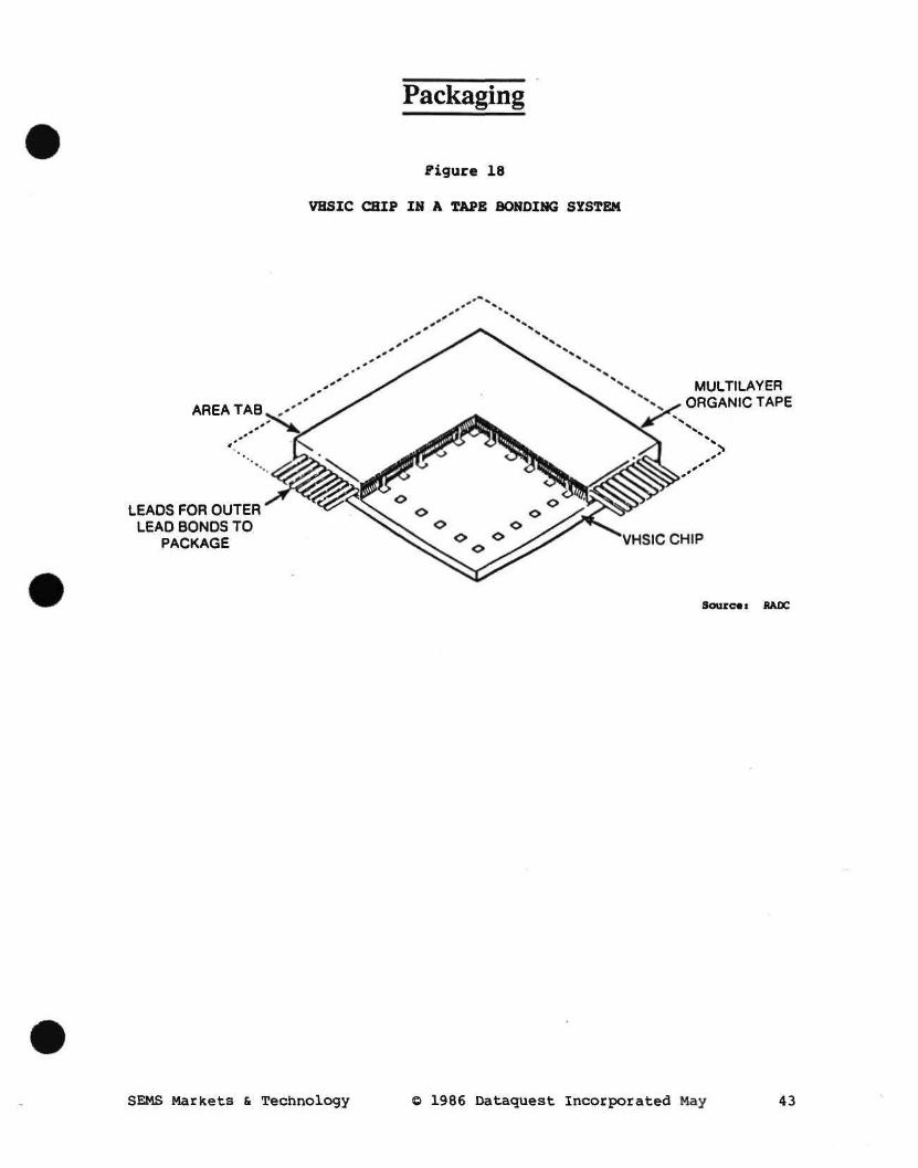
Packaging
Figure 18
VBSIC CBIP IN A TAPE BONDING SYSTEM
AREA TAB. ,'
LEADS FOR OUTER LEAD BONDS TO
PACKAGE
MULTILAYER ORGANIC TAPE
VHSIC CHIP
Source I ilAOC
SEMS Markets & Technology © 1986 Dataquest Incorporated May 43

Packaging
Fl ip Chip
The flip chip assembly process was developed by IBM in the 1960s and is referred to as the "controlled-collapse" technique. The flip chip is basically a chip designed for facedown reflow soldering, as opposed to chip-and-wire devices, which require faceup wire bonding. The contact areas are prepared on the front or active side of the chip. Solder bumps for reflow connections are formed on the chips while in wafer form. The chip is then passivated with silicon nitride or quartz and made hermetic by the solder ball in the contact openings. Testing is accomplished through the solder bumps. After testing, the dice are placed in "flip" orientation (upside down) on the substrate and then the assembly is heated in a furnace to melt the solder. The surface tension of the solder aligns the dice properly to the substrate; tne alignment is retained as the circuit cools.
Although the flip chip assembly process is critical, as it must be carefully controlled in circuits to assure high quality and reliability, the flip chip technology offers many cost-saving advantages such as;
• Lower assembly costs using solder bumps instead of wire bonding
• Reduced labor and material costs as wire bonding is eliminated
• Improved yields through automated assembly
• Cost reductions realized through lower capital equipment requirements
Currently, the major users of the flip chip technique are Oelco and IBM.
44 © 1986 Dataquest Incorporated May SEMS Markets & Technology

Packaging
Fl ip Chip
The flip chip assembly process was developed by IBM in the 1960s and is referred to as the "controlled-collapse" technique. The flip chip is basically a chip designed for facedown reflow soldering, as opposed to chip-and-^ire devices, which require faceup wire bonding. The contact areas are prepared on the front or active side of the chip. Solder bumps for reflow connections are formed on the chips while in wafer form. The chip is then passivated with silicon nitride or quartz and made hermetic by the solder ball in the contact openings. Testing is accomplished through the solder bumps. After testing, the dice are placed in "flip" orientation (upside down) on the substrate and then the assembly is heated in a furnace to melt the solder. The surface tension of the solder aligns the dice properly to the substrate; the alignment is retained as the circuit cools.
Although the flip chip assembly process is critical, as it must be carefully controlled in circuits to assure high quality and reliability, the flip chip technology offers many cost-saving advantages such as;
• Lower assembly costs using solder bumps instead of wire bonding
• Reduced labor and material costs as wire bonding is eliminated
• Improved yields through automated assembly
• Cost reductions realized through lower capital equipment requirements
Currently, the major users of the flip chip technique are Oelco and IBM.
44 © 1986 Dataquest Incorporated May SEMS Markets & Technology


European Semiconductor Manufacturing
OVERVIEW
The European market for semiconductors amounted to an estimated $4.6 billion in 1985, approximately 19 percent of total worldwide consumption. About 20 percent of this market was for discrete devices, which is down from their disproportionately high percentage of 26 percent only two years ago in 1983.
In Europe, semiconductor manufacturing is performed both by European and U.S. companies. The U.S. companies have traditionally supplied 40 to 50 percent of this market. Unlike in the United States, few companies in Europe focus only on semiconductor manufacturing. Most large semiconductor manufacturers in Europe are divisions of large, industrial electronic systems manufacturers.
Recent Decline in Worldwide Share
Over the past several years, the European semiconductor market has declined in dollar terms as a percent of total world semiconductor consTimption. In 1979, European consumption represented 27 percent of the worldwide market; in 1985, European consumption represented only 19 percent.
In 1978, three European companies ranked among the top 15 worldwide semiconductor manufacturers—by 1985, only one remained in the top 15. In the key new product area of MOS integrated circuits, the European companies' 1985 share was approximately 4.7 percent.
Part of this decline was due to the fall of the European currencies vis-a-vis the U.S. dollar, but there were also other problems. Because of a narrow market base, a lack of international product strategy, and a lack of competitiveness, European semiconductor companies failed to keep pace with product and manufacturing advances.
In many instances, the European semiconductor companies are able to compete against their larger and more cost-effective U.S.-owned competitors only because of subsidies granted by their respective national governments.
SEMS Industry Econometrics © 1986 Dataguest Incorporated July

European Semiconductor Manufacturing
Historically, most European semiconductor companies have not fully developed their international manufacturing and marketing capabilities. This lack of international reach, together with the greater market strength and advanced technology of U.S. manufacturers, has contributed to the weakened competitive condition of many European companies. However, there are exceptions to this rule. Phillips, Siemens, and now Thomson, through its acquisition of Mostek, have attained strong international positions.
Revitalization and Growth of the European Industry
There are encouraging signs that the European semiconductor industry is beginning to overcome some of the bonds that have restricted its market share. Of the total semiconductor production in 1985 ($24,542 million), European companies accounted for approximately 12 percent ($2,850 million). This was the first time in 10 years that European companies gained market share and represents a beginning of a payback on their commitment to capital and R&D investments. By 1990, the European companies' market share could be as high as 15 percent.
Although historically there have been few start-ups in Europe, this is changing. Though not as prolific as in the United States, these European start-ups are showing significant activity, which Dataguest believes represents a fundamental change in the European industry. Integrated Power Semiconductor, Matra-Harris, and Mietec have already made substantial progress in their respective fields, and a new venture, European Silicon Structures (ESS), was launched recently.
Some European companies have recognized their lack of international reach and have created strategic alliances to remedy this shortcoming. For example, the Phillips-Siemens mega-project will result in Europe having a state-of-the-art process capable of building 4-megabit DRAMs and 1-megabit SRAMs. In addition, Thomson in France and MEDL in the United Kingdom have announced a development project to cooperate on ASICs. Similar agreements exist between Thomson and Oki, S6S and Toshiba, and Phillips and Texas Instruments.
European companies are determined to be major players in the worldwide semiconductor industry. In addition to managerial talent, European companies also have impressive R&D and financial capabilities. Most importantly, European electronics companies and their governments are committed to having a world-class electronics industry.
© 1986 Dataquest Incorporated July SEMS Industry Econometrics

European Semiconductor Manufacturing
CAPITAL SPENDING
In 1985, European companies invested $381 million in new-semiconductor equipment, while North America invested $2,211 million and Japan invested $3,346 million. Dataquest estimates that the 1986 numbers will be $430 million, $2,193 million, and $2,980 million, respectively. Furthermore, we believe that as a percent of revenue, European investment will remain below that of both North America and Japan (see Table 1 ) .
Table 1
ESTIMATED CAPITAL VS. REVENUE: NORTH AMERICA, JAPAN, AND EUROPE 1985-1990
(Millions of Dollars)
1985 1986 1987 1988 1989 1990
North American Revenue $11,272 $14,209 $18,329 $22,518 $22,622 $26,584
Capital Spending $ 2,211 $ 2,193 $ 3,569 $ 4,579 $ 4,528 $ 5,410 Capital/Revenue 20"^ 15% 19% 20% 20% 20%
Japanese Revenue $10,185 $11,600 $15,494 $20,291 $21,962 $26,584 Capital Spending $ 3,346 $ 2,980 $ 3,905 $ 4,495 $ 4,679 $ 5,509 Capital/Revenue 33% 26% 25% 22% 21% • 21%
European Revenue $ 2,301 $ 2,732 $ 3,780 $ 5,031 $ 5,398 $ 6,573 Capital Spending $ 381 $ 430 $ 589 $ 817 $ 950 $ 1,119 Capital/Revenue 17% 16% 16% 16% 18% 17%
Source: Dataquest May 1986
R&D ACTIVITIES
In addition to individual company efforts, European R&D advances are being lead by both government initiatives, and by joint, private initiatives.
SEMS Industry Econometrics 1986 Dataquest Incorporated July

European Semiconductor Manufacturing
Governmental Initiatives
The competitive weakness of the European semiconductor industry has not been helped by the attention European governments have traditionally given the politically more powerful industries. For example, the European Economic Community (EEC) spends much more on farming than on semiconductor technology, despite enormous agricultural stockpiles.
Fears of creating unemployment are also very acute in Europe. Unemployment is now in the area of 11 percent and is expected to remain high throughout the 1980s. Many Europeans look only at job displacement and not at job creation and fear that increased emphasis on high technology will increase the unemployment rate.
In spite of the difficulties encountered in funding high-technology enterprises, the European community recognizes the importance of technological growth and is now moving toward the deliberate cultivation of high technology. For example, in early 1984, the EEC approved ESPRIT (European Strategic Program for Research and Development in Information Technology), a $1.3 billion electronics R&D program in five research categories: advanced microelectronics, software technology, advanced information processing, office automation and computer integrated manufacturing, and information exchange systems.
Private Initiatives
Twelve leading European-owned computer and communications manufacturers have agreed to start using international standards that are designed to enable their products to be interconnected.
A European venture capital initiative called Euroventures BV was undertaken in mid-1984. The subscription goal is $100 million, of which $30 million is already committed. Euroventures will make investments through several independently managed satellite funds. Its overall goal is to strengthen and develop Europe's industrial and technological base by creating less-fragmented markets.
THE EUROPEAN SEMICONDUCTOR MARKETPLACE
The use of semiconductor devices in Europe is heavily weighted toward industrial, telecommunications, and consumer uses (over 65 percent) with smaller markets for computer and military applications (29 percent).
1986 Dataguest Incorporated July SEMS Industry Econometrics

European Semiconductor Manufacturing
Automotive
Although Europe lacks the incentives of strong antipollution requirements, Dataquest thinks that the drive for fuel conservation will cause above average growth in the automotive semiconductor market. Total semiconductor automotive sales were approximately $256 million in 1985, and we expect growth to $599 million in 1990, a compound annual growth rate (CAGR) of 19 percent. This is higher than the Dataquest consumption forecast of 15 percent CAGR over the same period for the European semiconductor market as a whole.
Computer
U.S. companies such as Burroughs, Digital Equipment Corporation, Honeywell, and IBM traditionally have dominated the European computer market. These companies all have extensive R&D, engineering, and manufacturing capabilities in Europe. Only Cii Honeywell Bull (France), ICL (the United Kingdom), and Siemens (West Germany) remain strong in the European mainframe computer market.
However, European companies are more active in the data processing area. Market participants include: Cii Honeywell Bull (France), GEC (the United Kingdom), ICL (the United Kingdom), Kienzle (West Germany), Matra (France), Nixdorf (West Germany), Olivetti (Italy), Olympia (West Germany), Phillips (the Netherlands), Siemens (West Germany), Thomson (France), and Triumph-Adler (West Germany).
Although the emerging business personal computer area is currently dominated by Apple and IBM, there has been emerging strength exhibited by ACT (the United Kingdom), Olivetti (Italy), Siemens (West Germany), and Thomson (France).
Dataquest forecasts that European electronic data processing semiconductor consumption will increase from $256 million in 1985 to $599 million in 1990, demonstrating a 17 percent CAGR.
Consumer
Led by the television manufacturers and supported by makers of audio equipment and domestic kitchen appliances, Europe has always been strong in the consumer market. More recently, Europe has developed a strong home computer manufacturing industry, particularly in the United Kingdom, led by manufacturers such as Acorn, Amstrad, Oric, and Sinclair (Sinclair was recently purchased by Amstead).
SEMS Industry Econometrics © 1986 Dataquest Incorporated July

European Semiconductor Manufacturing
These markets, however, remain vulnerable to Far Eastern imports. Dataquest therefore expects a below average growth in consumer end-user semiconductor consvimption (15 percent CAGR) and estimates that this segment will grow from $906 million in 1985 to $1,782 million in 1990.
Military
This segment accounted for approximately 10 percent of the total 1985 European semiconductor constimption. Dataquest forecasts that total European government and military semiconductor constimption will increase from $449 million in 1985 to $910 million in 1990, a 15 percent CAGR.
Industrial
The industrial end-user category represented 22 percent of the total 1985 European semiconductor consumption. Industrial semiconductors are used in areas such as: image recognition systems, robotics, office automation, automatic test equipment, and advanced machine tools. Dataquest expects industrial end users to remain a major market area, and forecasts growth from $1,035 million in 1985 to $2,219 in 1990, a 16 percent CAGR.
Teleconmwinications
The European telecommunications semiconductor market is the world leader, representing 25 percent of the total European semiconductor market in 1985. The advent of cost-competitive CMOS and power devices, with all their benefits of low-power consumption and supply tolerance, has enabled European companies to gain a strong place in the telecommunications end-equipment markets.
M2uiy worldwide semiconductor producers are developing and producing high-volume dedicated semiconductors for telecommunications use. Dataquest expects the European telecommunications market for semiconductors to grow at a 17 percent CAGR between 1985 and 1990.
SERVICES AND SUPPLIERS TO THE SEMICONDUCTOR IMDUSTRY
Semiconductor capital equipment is primarily supplied by U.S.-owned companies. Although Canon, Hoya, and Nikon are active in the European market, overall there is a low level of participation by Japanese companies. Dataquest believes that the low level of Japanese participation in the European market is due to the absence of a European-based sales and service support organization. Japanese firms typically want such support in place before making substantial product offerings.
i © 1986 Dataquest Incorporated July SEMS Industry Econometrics

European Semiconductor Manufacturing
Assembly
Because high-volume assembly is still best carried out in the low labor cost areas, there are as yet no major independent assembly services developed in Europe.
Although there are some advantages (shorter product pipelines and fast turnaround time) in having both wafer fabrication facilities and assembly lines in Europe, most manufacturers install only pilot assembly lines.
However, the trend toward assembly automation and the present 14 percent import duty on semiconductor devices assembled outside of Europe are incentives for assembly to remain in the EEC. These incentives have caused NEC, Hitachi, and Toshiba to build highly automated assembly lines in Europe, particularly in the high-volume memory and microprocessor areas.
Dataquest believes that with packages becoming more complex and more diverse and with the increasing growth in application-specific integrated circuits (ASICs), especially in the low-volume end of the market, opportunities for European-based assembly facilities will become more viable.
Capital Equipment
The European capital equipment industry is typified by a high degree of fragmentation, with different companies specializing in different aspects of the market.
The European capital equipment market is dominated by U.S.- and Japanese-owned companies. This is because of the relatively small European-owned semiconductor manufacturing base, and because the U.S.-and Japanese-owned companies with manufacturing facilities in Europe tend to equip those facilities with the same equipment as they use in their domestic operations. European companies that are major worldwide market participants include: A.S.M. in CVD; Balzars in physical vapor deposition; Censor in lithography (now a part of Perkin-Elmer); E.T. Associates (Electrotech) in planar etch; Leybold-Hereaus in physical vapor deposition; Karl Suss in x-ray alignment; and Carl Zeiss, which makes some of the most advanced lenses in the world.
Materials
The materials market is similar to the capital equipment market in that no major company manufactures the whole range of products. Bulk gases, photomasks, silicon wafers, photoresist, and specialty gases have at least one major European supplier.
*
SEMS Industry Econometrics © 1986 Dataquest Incorporated July 7

European Semiconductor Manufacturing
European strength in the area of gases is based on the fact that some gases are consiuned in such vast quantities that is it necessary to produce them locally. In both masks and silicon, the high level of European-based wafer manufacture has created enough market leverage to justify European production. The relative decline of the European currencies since 1981 has given the European wafer manufacturers a considerable cost advantage over the other suppliers. Another factor contributing to the growth of the indigenous European mask-making industry is the ever-increasing need to reduce the time taken from design completion to first silicon, which is especially important for ASICs.
The major European-based suppliers of silicon wafers include Wacker-Chemie (West Germany), Topsil Semiconductor Materials (Denmark), and Dynamit Nobel Silicon (Italy). The major European-based suppliers of III-V materials include Wacker-Chemie (West Germany); ICI Wafer Technology (Imperial Chemical Industries) and MCP, Ltd., (both of the United Kingdom); and Boliden Finemet (Sweden).
BOC (British Oxygen Company, the United Kingdom), L'Air Liguide (France), and Linde A.G. (West Germany) are the major European-based suppliers both in specialty and bulk gases. Another major supplier of specialty gases in Europe is Messer Griesheim (West Germany).
The major European-based suppliers of photoresist products include Hoechst AG (West Germany), E. Merck (West Germany), and Micro-Image Technology (the United Kingdom). Merck and Hoechst are also major suppliers of process wet chemicals for semiconductor fabrication.
Hanomask (France); Compugraphics (Scotland); IC mask, a joint-venture of TSE and ICI (England); CSEM (Switzerland); and SAC, a newcomer from England, are the major European-based suppliers of photomasks.
Testing
Currently, there is no major market for independent semiconductor testing houses in Europe.
Due to the high capital cost of modern complex VLSI test equipment, Dataquest does not foresee much growth potential in the testing area, except perhaps as an integral part of an independent ASIC assembly facility.
© 1986 Dataquest Incorporated July SEMS Industry Econometrics

European Semiconductor Manufacturing
SEMICOIJIDUCTOR FAB DISTRIBUTION
Semiconductors are fabricated in 91 separate facilities in 17 different European countries. (See Table 2 for a listing of the individual companies, locations, products, and technologies). England has 22 fabs located on its soil as listed in Table 3, or approximately 24 percent of the total in all of Europe. The United Kingdom has 35 fabs within it, or approximately 38 percent of the European total. France has 16 fabs on its soil, or approximately 18 percent, and West Germany has 13 fabs, or approximately 14 percent of the total number of fabs in Europe (see Figure 1). England, France, and West Germany have a total of 51 fabs between them, or 56 percent of the total number of fabs in Europe.
Table 2
EUROPEAH FABS
Company
Acrian Analog Devices Ansaldo Array Logic Asea Hafo Austria Hicrosystems Brovm Boveri Burr Brown BE2 Fairchlld Paselec Favag Ferrantl General Instruments HMT Hughes Microelec IBM IBM IBM IBM Inmos Integrated Power Semiconductor Intel Int'l. Rectifier Iskra Isocom ITT
LSI Logic Lucas
Marconi Electronic Marconi Electronic Marconi Aesearch Center
City
Br Idgend Raheen Genoa Cambridge Jarfalla Unterpremstattn Turgi Livingston Aix-En-Provence Saint Etienne Zurich Bevaix Oldham Glenrothes Brugg Glenrothes Corbell-Essones Hannover Sindelfingen Boebllngen Newport
Livingston Tel Aviv Bprgarp Torines Trbovlje Hartlepool Freiburg
Braunschweig Sutton Coldfld
Lincoln Wembley
Chelmsford
Country Product Technology
Wales Microwave BIP Eire Digital, Linear, BPD HOS Italy Discretes OIS England Semlcustom N/A Sweden Memory, Discretes, LSI BIP, LIN, MOS Austria Custom LSI N/A Switzerland Discretes LIN Scotland Custom CMOS, BIP, LIN France Semlcustom N/A France LSI HOS Switzerland Custom LSI BIP, OIS, OPT Switzerland Custom LSI H/A England Digital, Cust<»i LSI BIP, HOS, OIS Scotland Memory HOS, CMOS Switzerland TV, Game and Telecom MOS Scotland LSI MOS, LIN France Diodes BIP West Germany Thyristors, Diodes, Rectifiers OIS West Germany 4 facilities HOS, BIP West Germany IC, Hybrid, Pwr. Discretes BIP, OIS Wales LSI HOS
Scotland Linear LIN Israel LSI MOS Italy OIS OIS Yugoslavia Digital, Discretes BIP, OIS England Opto GaAs West Germany Digital, Rectifier Pwr.
Trans., LSI BIP, OIS, HOS West Germany LSI HOS England GaAs, Pwr. Discretes,
Thyristors, Rectifiers GaAs, DIS England Discretes, MOS, LSI, Microwave OIS, MOS England LSI oiS, MOS
England N/A GaAs
(Continued)
SEMS Industry Econometrics 1986 Dataguest Incorporated July

European Semiconductor Manufacturing
Table 2 (Continued)
EUROPEAN FABS
Company
Matia-Harris Microelectronic-Mar in Mietec Mistral Mitel Motorola Motorola Motorola Mullard Mullard National Semiconductor NEC Nowmarlcet Microsystems
Philips
Philips Philips Philips Philips Piher Plessey Plessey Plessey Plessey III-IV Group Plessey Racal Rifa Rifa Robert Bosch RTC Seiaelab Semikron Senikron SGS
SGS SGS Siemens Siemens Siemens Siliconlx Standard Electrica STC Tag Telefunken Electronic Texas Instruments Texas Instruments Texas Instruments Texet
City
Nantes Marin Oudenaarde Sermoneta Caldicot Toulouse Bast Kilbride East Kilbride Southampton StocKport
Greenock Livingston
Nowmarket
Eindhoven
Nijmegen Stadskanaal Zurich Hamburg Granollers Caswell Plympton Swindon
Towchester Roborough Reading Kalmar Rista Reutlingen Caen Glenrothes Cricklade Nurnberg Rennes
Agrate Catania Villach Cricklade Munich Swansea Cascals FDotscray Zurich
Hellbronn Bedford Villeneuve-Ioub Freising Nice
Country
France Sweden Belgium Italy Wales France Scotland Scotland England England
Scotland Scotland
England
Netherlands
Netherlands Netherlands Switzerland West Germany Spain England England England
England England England Sweden Sweden West Germany Franca England England West Germany France
Italy Italy Austria England West Germany Wales Portugal England Switzerland
West Germany England France West Germany Prance
Product
SRAM, Gate Arrays Custom LSI ASICs Discretes Custom ICs Digital, Discretes, Linear GaAs FET Amps, LEOs, Microwave 256K and 64K RAM Digital, LSI Discretes
Digital, Linear, LSI LSI
Linear, Discretes
Discretes, Linear, LSI, Opto Discretes, Linear GaAs, Custom Digital, Linear, LSI Analog, Discretes, HOS Digital, Discretes, Linear Discretes, Opto, LSI LSI Digital, Diodes
N/A Analog LSI Power Capacitors Digital, LSI Custom LSI Discrete, Linear, LSI, Opt. Digital Discretes Discretes Discretes, Linear, Custom LSI LSI, Linear Digital, Std. Logic 64K 08AH, Discretes Discretes BPO, Digital, LSI, Opto Discretes, LSI Discretes Custom LSI Discretes
Linear, (^to Discretes, LSI Custom LSI, HOS LSI Digital, Linear Discretes
Technology
DIS, MOS N/A CMOS, HVMOS, BIMOS DIS BIP, LIN, OPT BIP, DIS, LIN GaAs MOS BIP, HOS DIS
BIP, LIN, MOS HOS
LIN, DIS
BIP, DIS, HOS BIP, DIS, LIN GaAs, OPTO, MOS BIP, LIN, HOS BIP, DIS, MOS BIP, DIS, LIN DIS, OPTO, MOS MOS BIP, LIN
GaAs BIP, DISC, LIN HOS DIS BIP, MOS BIP, MOS, DIS, LIN BIP, DIS, HOS BIP, DISC, LIN DIS DIS
DIS, LIN, HOS HOS, LIN BIP, OIS, LIN MOS, OIS OIS BIP, OIS, MOS DIS, HOS OIS HOS OIS
BIP, HOS, DIS DIS, HOS, OPTO HOS BIP, LIN OIS
(Continued)
10 1986 Dataguest Incorporated July SEMS Industry Econometrics

European Semiconductor Manufacturing
Table 2 (Continued)
EUROPEAN FABS
Company
Thomson Thomson Thomson Thomson Thomson Thomson Thomson CSP Valvo Velsala Westcode Semi. Wolfson Microelectronic
Aix Les Bains Aix-En-Provence Grenoble Rousset Saint Egreve Tours Massy Hamburg Helsinki Chippenham
Edinburgh
Country
France Prance France France Prance France France West Germany Finland England
Scotland
Product
Gate Arrays Thyristors, LEO, Diodes Memory, MPU 1.31, Memory, MPU Digital, Custom Discretes N/A Digital, Discretes, MPU LSI, Std. Cells Discretes
N/A
Technology
MOS DIS MOS MOS BIP, LIN DIS GaAs BIP, CMOS, OPT MOS, CMOS DIS
N/A
N/A - Hot Available
Source: Dataquest May 1986
SEMS Industry Econometrics 1986 Dataquest Incorporated July 11

European Semiconductor Manufacturing
Table 3
DISTRIBUTION OF EUROPEAN SEMICONDUCTOR FABS
Country Fab Count
England 22 France 16 West Germany 13 Scotland 9 Switzerland 6 Italy 5 Wales 4 Sweden 4 Netherlands 3 Austria 2 Eire 1 Finland 1 Spain 1 Portugal 1 Israel 1 Belgium 1 Yugoslavia _1
Total 91
Source: Dataquest May 1986
12 © 1986 Dataquest Incorporated July SEMS Industry Econometrics

European Semiconductor Manufacturing
Figure 1
DISTRIBUTION OF EUROPEAN SEMICONDUCTOR FABS
Source: Dataquest July 1986
SENS Industry Econometrics 1986 Dataquest Incorporated July 13

C^i

Japanese Semiconductor Manufacturing
ECX)NOMIC STRUCTDKE OF JAPAN
Before discussing the Japanese market for semiconductor manufacturing equipment specifically, a brief overview of the major organizational features and trends of the Japanese economy is in order.
Industrial Groups
Japanese industry is organized into industrial groups. These industrial groups are clustered around the leading banks like Dai-Ichi Kangyo, Fuji, Mitsubishi, Mitsui, Sanwa, and Sumitomo. Today's industrial groups are different from the large, family-controlled trading blocks known as zaibatsu, which were formally dissolved after World War II. Industrial groups differ from the prewar zaibatsu in that councils of presidents (shacho~kai) have replaced the former holding companies.
Keiretsu Gaisho
A company in an industrial group is frequently the center of a keiretsu gaisho, which is a network of affiliated companies that are in turn affiliated with a large group of subcontractors.
The Ministry of International Trade and Industry (MITI)
The Ministry of International Trade and Industry (MITI) has evolved into the "general staff" for developing industrial policies (sangyo seisaku) and promoting foreign trade. MITI is responsible for assisting specific industries and guiding their expansion. It has done this by shielding Japanese manufacturers with import protectionist policies until they have attained a competitive high-volume base. Then MITI directly promotes exports through direct subsidies, tax incentives, and targeted R&D. It is the key ministry behind Japan's challenge in the semiconductor field.
Japanese R&D trends are heavily influenced by government sponsorship and funding of basic research projects. The Japanese government is currently pursuing a series of joint industry/government R&D programs aimed at accelerating the rate of Japan's technological innovations. The major sponsors of these programs are MITI and Nippon Telegraph and Telephone (NTT).
For example, in 1976, MITI and NTT formed the VLSI Technology Research Association, which consisted of both government agencies plus Fujitsu, Hitachi, Mitsubishi Electric, NEC, and Toshiba. The association's goal was to develop basic VLSI (very large scale
SEMS Industry Econometrics © 1986 Dataquest Incorporated Jan. 10 ed.
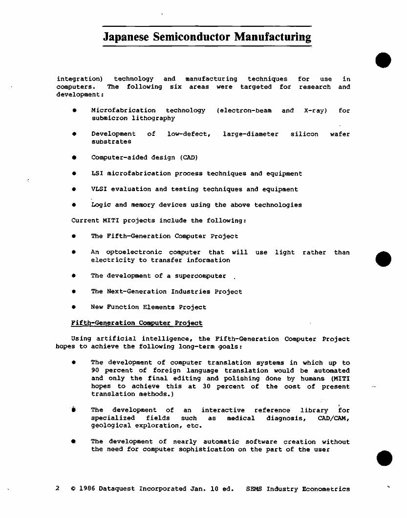
Japanese Semiconductor Manufacturing
integration) technology and manufacturing techniques for use in computers. The following six areas were targeted for research and deve opment;
Microfabrication technology (electron-beam and X-ray) for submicron lithography
Development of low-defect, large-diameter silicon wafer substrates
Computer-aided design (CAD)
LSI microfabrication process techniques and equipment
VLSI evaluation and testing techniques and equipment
Logic and memory devices using the above technologies
Current MITI projects include the following:
The Fifth-Generation Computer Project
An optoelectronic computer that will use light rather than electricity to transfer information
The development of a supercomputer .
The Next-Generation Industries Project
New Function Elements Project
Fifth-Generation Computer Project
Using artificial intelligence, the Fifth-Generation Computer Project hopes to achieve the following long-term goals:
• The development of computer translation systems in which up to 90 percent of foreign language translation would be automated and only the final editing and polishing done by humans (MITI hopes to achieve this at 30 percent of the cost of present translation methods.)
• The development of an interactive reference library for specialized fields such as medical diagnosis, CAD/CAM, geological exploration, etc.
• The development of nearly automatic software creation without the need for computer sophistication on the part of the user
2 © 1986 Dataquest Incorporated Jan. 10 ed. SEMS Industry Econometrics

Japanese Semiconductor Manufacturing
Research is being pursued in problem-solving and inference systems, knowledge-based systems, intelligent human/machine interface systems, development support systems, and basic applications systems.
Optoelectronics
MITI hopes to develop a computer that will use light rather than electricity to transfer information. To achieve this goal, the Optical Measurement and Control System was formed in 1979 to develop optical elements for sensing devices (image processing) and data transmission.
Supercomputer
By 1989, MITI hopes to develop a supercomputer that can perform 10 billion floating-point operations per second (GFLOPS), opening the way for scientific applications not currently possible, such as simulating atmospheric movement and analyzing satellite-transmitted photographs.
Next-Generation Industries Project
Sponsored by the National Research and Development Program, the Next-Generation Industries Project will run from 1981 to 1990. Fifty-eight participating companies are assigned to five research associations (three in new materials, one in biotechnology, and one in new semiconductor function elements) that are commissioned to conduct basic research.
The New Function Elements Project
The New Function Elements Project is Japan's next step in developing semiconductor technology. Organized by MITI, its members include Fujitsu, Hitachi, Matsushita, Mitsubishi, NEC, Oki, Sanyo, Sharp, Sumitomo Electric, and Toshiba. Its goals include the development of:
$ Lamination techniques for building multiple-layer structures in which each layer is one atom thick
• The development of techniques for reducing cathode-to-anode distance within individual semiconductors to within 5,000 angstroms
• The development of methods for incorporating IC elements into chips in layers to increase the density of elements by 40 to 50 times, with specific targets including 8- to 10-layer elements integrating logic, memory, and other functions, and 5-or-more-layer elements with sensing and signal switching
SEMS Industry Econometrics © 1986 Dataquest Incorporated Jan. 10 ed.

Japanese Semiconductor Manufacturing
It also has the goal of developing element, mounting, integration, and evaluation technologies with the ultimate aim of producing highly integrated ICs that are capable of withstanding extreme heat and radiation.
The Long-Term Industrial Technology Planning Committee (a planning and study committee of academics and experts commissioned by MITI) recently recommended that research in the 1990s be conducted in the following areas:
• Microtechnology—Billion-byte ICs (block line), genetic engineering
• Information technology—Artificial intelligence and organic superconductors using genetic engineering as an area of information technology
•' Composite technology—Advanced mechantronics, large integrated systems for hostile industrial environments
NTT
NTT is currently developing a nationwide Information Network System (INS) that is designed to lay the foundation for Japan's communications system in the twenty-first century. Two major components of this system are the CAPTAIN (Character and Pattern Telephone Access Information Network) System and the DDX (Digital Data Exchange) Packet Switched Network. These systems will be connected to telephone and television channels to develop a Home Information System by the 1990s.
SEMICONDDCTOR INDUSTRY
Because of government-sponsored R&D projects and intercompany rivalry, Japanese semiconductor technology is moving at an extremely fast pace. In early 1983, several Japanese companies introduced their new 256K dynamic RAMs.
The following companies all have 1-megabit DRAMs in various stages of development: Fujitsu, Hitachi, Mitsubishi Electric, NEC, NTT, and Oki Electric. Toshiba is now producing 1-megabit DRAMs in volume production. A comparison of Japanese 1-megabit DRAMs from four of these companies is given in Table 1.
4 © 1986 Dataquest Incorporated Jan. 10 ed. SEMS Industry Econometrics

Japanese Semiconductor Manufacturing
Table 1
COMPARISON OF SEIJBCTED JAPANESE 1-MEGABIT DRAMS
Toshiba Hitachi
•
Process
Design Rule (Microns)
Organization
Chip Size (mm)
Cell Size (um)
Access Time (ns)
Cycle Time
Power (active/standby)
Packaging
300-mil DIP
NMOS NMOS
NEC
NMOS
NTT
CMOS
1.2 1.3 1.0 0.8
1Mb X 1 1Mb X 1 128K x 8 1Mb x 1
4.78 X 13.2 4.76 x 9.86 9.2 x 8.07 6.4 x 8.2
5.0 X 6.4
70
N/A
270/15mW
18-pin,
300-mil
3.0 X 7.0
90
260
300/lOmW
18-pin,
DIP
5.5 X 8.0
120
300
290/15mW
30-pin,
N/A
3.7 X 5.4
140
350
250/5mW
N/A
/A
N/A = Not Available
Source: DATAQUEST August 1985
Fujitsu recently announced a 128K EPROM and a 288K CMOS EPROM; Toshiba, a multichip 256K EPROM; and Hitachi, a 128K EPROM. We believe that the trend toward higher densities and CMOS logic will continue unabated.
Gate arrays are also experiencing rapid growth in Japan. All major Japanese semiconductor manufacturers have jumped into production. However, they are unable to meet domestic market demand because of the large internal demand in their captive markets.
SEMS Industry Econometrics © 1986 Dataquest Incorporated Jan. 10 ed.

Japanese Semiconductor Manufacturing
Japanese firms are rapidly moving into gallium arsenide (GaAs), which promises even faster speeds for proposed supercomputers. Table 2 lists the GaAs facilities in Japan. Fujitsu has announced a direct-coupled high-electron mobility transistor (HEMT) logic designed on a GaAs substrate with a switching speed of 12.8 picoseconds (ps). We believe that Japanese industry may attempt to leapfrog CMOS technology by rapidly reducing the production cost for GaAs, a direction that has been signaled by the Optoelectronics Project's recent announcement of a computerized method for growing GaAs single crystals.
Table 2
JAPANESE GALLIUM ARSENIDE FACILITY LOCATIONS
Company
Canon Fujitsu Yamanashi Electric Furukawa Electric Co. Hitachi Maribeni Corp. Matsushita Electronics Mitsubishi LSI R&D Lab NEC NTT Atsugi Electric Communication Labs New Japan Radio Company Oki Research Lab Sanyo Sharp Electronics Corp. Showa Denko Sony Corp. Research Center Sony Corp. Semiconductor Toshiba R&D Center
Region
Kan to
Kanto Kan to Kanto Kinki
Kinki
Kinki Kanto
N/A
Kanto Kanto Kinki
Kinki Kanto
Kanto
N/A Kanto
Prefect
Tokyo
Tokyo Tokyo Tokyo Osaka
Osaka
Hyogo Tokyo
N/A
Saitama Tokyo Osaka
Osaka Tokyo
Kanagawa
N/A Kanagawa
City
Tokyo
Tokyo Tokyo Tokyo Osaka
Osaka
Hyogo Tokyo
Atsugi
Kawagoe Tokyo Osaka
Osaka Tokyo
Yokohama
Atsugi Kawasaki
N/A = Not Available
Source: DATAQUEST December 1985
6 © 1986 Dataquest Incorporated Jan. 10 ed. SEMS Industry Econometrics

Japanese Semiconductor Manufacturing
In the area of bipolar digital ICs, Japanese companies will continue to be competitive in advanced transistor-transistor logic (TTL) and emitter-coupled logic (ECL) and in bipolar RAMs, PROMs, and gate arrays. Major manufacturers will follow the U.S. lead in advanced TTL devices, especially Texas Instruments' Advanced Schottky (AS) and Fairchild's Advanced Schottky (FAST), and offer compatible devices as second-source suppliers. Japanese research in ECLs is heating up because of their potential use in supercomputer systems.
Ne<roomers and Start-ups
Table 3 lists recent newcomers and start-ups in the Japanese semiconductor manufacturing industry. Newcomers far outnumber start-ups. Newcomers are established companies from other industries that are moving into the semiconductor industry. Thus, 1984 witnessed several companies from the watch and calculator industry move into CMOS memory, logic, and gate arrays. The same year saw companies from heavy industry, Minebea, for example, move into MOS memory using technology transfer.
Table 3
JAPANESE NEWCOMERS AND START-UPS
Company
Fuji Electric New JRC Rohn Sanken Shindengen Sony Stanley Suwa Seikosha Minebea Casio Pioneer Ricoh Yamaha NMB Semiconductor A&D Company Alpha Electronics Kyoto Semiconductor
1984 Sales (Millions $)
$211 $ 66 $241 $161 $106 $177 $ 41 $136 N/A N/A N/A $ 32 N/A N/A N/A N/A N/A
Largest Product Area
Discretes Linear ICs Linear ICs, Discretes Discretes Diodes Linear ICs Optoelectronics MOS Logic MOS Memory 64K/256K DRAMs CMOS Memory Gate Arrays CMOS Memory Gate Arrays CMOS Memory Logic CMOS Memories AID, D/A Converters Precision Resistors Optoelectronics
N/A = Not Available
Source: DATAQUEST August 1985
SEMS Industry Econometrics © 1986 Dataquest Incorporated Jan. 10 ed.

Japanese Semiconductor Manufacturing
SEMICONDUCTOR MANDFACTDRING EQUIPMENT
Japanese semiconductor capital investment grew 15.5 percent annually between 1973 and 1977. Total capital spending for the 10 major Japanese firms jumped 369 percent from 1978 to 1982.
Materials
The yields for Japanese 64K DRAMs are about 10 percent higher than those of U.S. and European manufacturers who use the same production equipment. This difference can be partly attributed to advances in material technology. Japanese manufacturers tend to place more importance on chemicals (including photoresist) that have a higher degree of purity. Japanese manufacturers also use more glass (which has very low expansion properties) for photomasks.
Wafer Processing
Demand for wafer steppers is growing rapidly. At present, steppers are being supplied by Perkin-Elmer's recently acquired Censor Corporation (distributed exclusively through Hakuto); Eaton Optimetrix (distributed exclusively through C. Itoh); GCA (distributed exclusively through Sumitomo Corporation); Hitachi Ltd.; Nippon Kogaku K.K. (Nikon); and Ultratech, a division of General Signal (distributed exclusively through Omron Tateisi Electronics Co.). We believe that Canon, which now has a dominant market position in contact/proximity aligners, will also make inroads into the stepper market shortly.
The demand for 5X steppers is rapidly increasing in Japan, and we believe that there may be a shortage of these items. To lessen stepper shortage problems, manufacturers have begun to employ a mixture of contact/projection aligners and steppers. The extent of mixing, and matching varies with the individual manufacturer. Generally speaking, steppers are used to form the more sophisticated areas such as gates and the polysilicon layer, while contact/projection aligners are used to form electrodes.
Etching
Japan has witnessed improvement in the technologies of etching, film deposition, ion implantation, and sputtering. In the area of dry etching, reactive ion etching has been used in aluminum film etching to produce 64K DRAMs. Low-pressure chemical vapor deposition (CVD) has been introduced by Kokusai Electric and Tel/Thermco; ion implantation by Eaton, Ulvac, and Varian; and sputtering by Anelva, MRC, Tokuda, and Ulvac.
8 © 1986 Dataquest Incorporated Jan. 10 ed. SEMS Industry Econometrics

Japanese Semiconductor Manufacturing
Assembly
The trend in assembly technology is toward higher speed and higher reliability. Automation is widely used in the scrubbing and die-bonding processes.
Testing
Cost reduction is particularly important in the testing area. At present, it is possible to test eight devices simultaneously. We expect Takeda Riken to successfully develop the technology to examine 16 devices simultaneously in the near future.
SBgQONDOCTOR PLANT DISTRIBUTION
There are approximately 140 semiconductor plant locations in Japan (see Table 4). There are eleven geographic regions in Japan including Okinawa (see Figure 1). Table 5 and Figure 2 provide a breakdown of semiconductor plants by these regions. The Kanto region, which includes the prefectures of Chiba, Gumma, Ibaraki, Kanagawa, Saitama, Tochigi, and Tokyo, has almost twice as many locations (25 percent of the total) as any other single region. (See Figures 3 through 11 and Table 5 for the distribution of plants by prefecture within a region.)
SEMS Industry Econometrics © 1986 Dataquest Incorporated Jan. 10 ed.

Table 4
JAPANESE SEMICONDUCTOR FABRICATION PLANT LOCATIONS vo CD
o\ a 01 n (u
tQ
c (D CO f t D O o t-l 'O
o 0)
n <D
a
o> 3
(D
CO
Ui
3 a c D) rt I I td o o 3 O 3 (D n-i-i H-
o 01
Coapany Region Prefecture
Falrchlld Falrchlld
Fuji Electric Fuji Electric Fuji Electric Fuji Electric Fuji Xerox Fujitsu Fujitsu Fujitsu Fujitsu Fujitsu Fujitsu Fujitsu Fujitsu Fujitsu VLSI Fujitsu yaaanashi Electric Hitachi Hitachi
Hitachi Hitachi
Hitachi Hitachi Hitachi Hitachi Hitachi IBM International Microtech Kodenshl No. S Plant
Matsushita Matsushita
Matsushita Matsushita
Matsusklta Matsushita Matsushita
Matsushita Matsushita Mitsubishi Mitsubishi Mitsubishi Mitsubishi Mitsubishi Mitsubishi Mitsubishi Mitsubishi
Mitsubishi Httsubishl
Mitsubishi
Electronics Electronics Electronics
Electronics Electronics
Electronics Electronics
Electronics Electronics
Ryushlj Kyushu
Tbsan Tosan
Tosan Tosan
Tokal Tosan Tohoku Tohoku Kan to Tohoku Tokal Tohoku Tohoku Tosan
Tosan Kanto Kan to Tohoku
Kanto Kanto Tosan Tosan Hokkaido Hokkaido Kinkl Tosan Kinkl Hokurlku Uokuriku
Hokuriku
Kinkl Hokurlku
Hokurlku Hokuriku Hokuriku Hokurlku Kyushu
Kinkl Kinkl Shikoku Shikoku Kyushu Kyushu Shikoku
Kyushu Shikoku
N/A
Nagasaki Nagasaki
Nagano Nagano Nagano Yaaanashi HIE Yaaanashi Fukushiaa Fukushiaa Kanagawa Fukushiaa NIE Iwate Iwate Gifu Yaaanash i Chlba Chlba Akita Tokyo Guaaa Yaaanash1 Yaaanashi Hokkaido Hokkaido Shiga Nagano Kyoto
Toyaaa Toyaaa
Nilgata
Kyoto Nilgata Toyaaa Toyaaa
Nilgata Toyaaa Fukuoda Byogo Hyogo Kochi Ehiae Ruaaaoto Fukuoda Ehlae
Fukuoda Ehiae
H/A
Isatiay4 Isa^Aya HatStlBOtO
Katsuaoto KatsuBoto Yawl Flash! SuEuka H/A Zulu Mo. 2 Pla Aliu Kawasaki A11 u-Ha Ic a aa tsu Tado Ivata EanegasaJc 1 riinoksKi Shova Hobaia Mobara Naka HUHSShl
Takaaakl JCof u Kofii
Chltose Chitose Yasu Kitalna Kyoto
Ouzu Ouzu
Aral
Nagaokakyo Aral Ouzu Ouzu
Aral Ouzu N/A N/A Kltaltaal Kagaai Waijo Kuaaaoto Fukuoda Sanjo Fukuoda N/A Kouchi
ProdLtcta
2SGK, 6SK SEUH
Blgh-speed TTL TRAHS TRN, DIO THH H/H OFT GaAs, TRANS Resaarch MBt, LOG, MPU, M W , LOQ, MPU, HPU, LOGIC NB(, LOGIC MM Ha, UK DRAHi Research LOG HOS, KBI
HEM N/A HBi, LOG, LIN, LOG, Mat, LIN, Hot, MPU, LOGIC S*f. DHAHs H/A MB( HB4 TRAMH, DIO, OPT SIP, TRANS
N/A HEN M94, HPU
HO), LOG, MPU, 64K DftAMS LIN HPU, UJGIC
HEN, LOG, HPU, 256K, E4K ORAM, LOG, LIN
TRANS, DIO, OPl LOG, TRANS, DIO HPU 25«K QRAM HEM, LOG, MPU, LOG, TRAMS, DIO
HBA Research Research
WU
TTL Gates TRANS
im: um4
• •
MPU,
*B«. mk,
DIO,
ibio 010
OPT TRAMS, DIO
LIH,
LIN HPU
LIN
TRA, 010
Technoloqv
HOS BIP MOS LIN MOS N/A OPT LIN, N/A HOS,
MOS, HOS MOS MOS HOS MOS, MOS HOS HOS N/A HOS, MOS, HOS, HOS N/A MOS HOS OIS, BIP,
N/A MOS BIP,
HOS, BIP LIN HOS BIP, HOS BIP,
DIS HOS, N/A HOS MOS, BIP, MOS N/A N/A MOS
OPT
BIP, BIP,
BIP
BIP,
BIP, BIP
OPT DIS,
MOS BIP,
MOS,
LIN
DIS
BIP, DIS
DIS DIS
LIN LIN
OPT
DIS
DIS
LIN
(Continued)

en
CO
M 3 a c m rf i-i *< a o o 3 O 3 (D f t i-l H-O 01
©
vo CO
a\ a 0) r t Di iQ c (D (0 rl-D
n O i-l •O o n 0) f t <D
a C-l 0) 3
(D
Table 4 (Continued)
JAPANESE SEMICONDUCTOR FABRICATION PLANT LOCATIONS
Company
Hitaublshl
Hitsubishi Mlcaual Electric Motorola Motorola Motorola NBC NBC NBC NBC NEC NBC NBC NBC NBC NBC NEC NEC NEC NBC NBC NBC NEC New Japan Radio Haw Japan Aadio Mvw Japan Radio Haw Japan Radio Nlhon Staiconductor
Hllgata Sanjo Danahi Hippcn (»aklcl Hlppon Gakhl Nippon PiEClalon Circuits Hlppon PraclAion Circuits NHfi Saalconductor NHB Scalconductor NKB Saul conductor 0J(1 Blactrlc 0*1 Electric Okl Blactrlc Okl Blectrlo OKI Blactrlc
Origin Blactrlc .Plcnaac Elactttd^
Ricoh Jilcoh
Roh» JtohB Roha
*
Reqlon
Kyushu
Shlkoku Kanto Tohoku Tbhoku Tohoku
Chugoku TDhoku Kanto Kyushu Kyushu Kinkl
Kyushu Chu90ku Tohoku
Kinkl
Kyushu Tohoku Kinki Klnki Kanto Kanto Kinki Kanto Kanto Kanto
Kanto Kanto
Hokuriku Kyushu
TOkai Kanto Kanto 'Kanto Kanto Kanto Tohoku Kyushu Kanto Kyushu Kyushu Kanto Tosan Kinkl Klnki
Kyushu Klnki liinki
Prefecture
Fukuoda
BhiM Kanagawa Hiyagl Fukushiaa Pukushiaa Yewaguchl Yaaagata Kanagawa Kuaaaoto Kagoshiaa Osaka
Kuaaaoto Yaaaguchl Yaaagata
Shiga Kuaaaoto Xaaagata
Shiga N/A Kanagawa Kanagawa N/A Saitaaa
Siitaaa Saitaaa
Saitaaa Ibaraki
Nilgata Kagoshiaa Shlzuoka Guaaa Tochlgl
Chiba Tokyo Chlba Hiyagl ' Mlyazakl Tokyo Mlyazakl Mlyazakl Tochlgl Yaaanaahi Osaka
Osaka Fujuoka
Kyoto Okayaaa
City
N/A Sal jo Ataugi Izuai City Alzu Aizu Yaaaguchl Tsuruoka Sagaaihara
Kyushu Kagoshiaa N/A Kuaaaoto Yaaaguchl Yafflagata
Ohtsu N/A Takahaaa Yokkalchl Ransal Taaagawa Saganihlara Kansal Kawagoe Kawagoe Kawagoe
Kawagoe N/A Nligata Kagoshiaa
Toyooka N/A Shiobara
Tateyaaa Tokyo Tateyaaa Miyagi N/A Tokyo Mlyazakl Mlyazakl Maaada Koufu Ikeda
Ikeda Aaagal Kyoto Ihara
ProdSiH:*
UX3 e4K DRAM Ke search HOS, BIP, HFU Km, HOI, MOS, N ^ N/A Hat, LOG, HPU Lit), TRANS HSI, lOG HOS, H£K, HPO, lOQ DIO, OPT TRAHS, DIO, OPT HBi, HPU, [OG K/A HOS, LOG, LIN, TRAHS
HBI, HPd, LIN, TRAK3, DIO
N/A BIF, Wa, LIN, TRANS HOS, Hat, TRANS, DIODBS TRAMS, DIO HQ(, LOS, LIH, DIS
LOG HS* HOS, LOG, LIN, TRANS, OPTO
GiAs, TRANS, DIO, OPT N/A N/A LOG HOt, UX;, HPU HOS, LOG, LIN
BIB, LOG, HOS, LOG, LIH, TOMS LOG Basaarch
25GE OtOS RAH, 64K, FAST S CXOS Heaoriea MBH Hat, HPU, LOC H ^ , HPU not, LOG, HPU, LIN, TRANS, DIO Hai, HPU 25M, 6iK DRAH, ^W SRAH IWUIS, DIO CuatoB LSI, SAH Device HOS, H£K, HOS, HFU HBH
TRANS BIP, U>G, LIN, OPT TRANS
Technoloqy
BIP,
HOS N/A HOS, HOS H/A »K}S LIN, HOS, HOS, DIE LIH,
MOS N/ft HOS, HOS,
W/A BIP, K03, DIS HOS HOS HOS HOB, LIH N/A GaAs HOS HOS HOS, BIP, HOS, N/A HOS HOS HOS HOS HOS HOS, HOS HOS DIS N/A HOS Wis DIS BIP, N/A
HOS
BIP
DIS BIP BIP
OPT
DIS, BIP,
LIN, DIS
DIS,
DIS HOS, LIN
BIP,
DIS,
LIH LIH
DIS
OPT
DIS
DIS
OPT
(Continued)

Table 4 (Continued)
JAPANESE SEMICONDUCTOR FABRICATION PLANT LOCATIONS
vo 00
o D 0> n-cu •Q c a> m f t
3 O O •1 '0 0 n 01 (T (D Qj
C^ 01 3
(D Oi
Ui
cn H 3 a c CO
n->< H O o 3 O 3 (D fil l H-O CO
CoKiany
8(nkait El*ctrlc Banlian tlmotc la SanKen ll«trlo Bankan tlactrle Sanki Bnginaaring Salka InatiuiaanEB Sharp Sharp sharp Sharp Sharp
Shtndan^sn Blactrlc Sony
atenlsy Electric
B tan lay ElacUtc Stanlay Electric Suva Balkoaha
Suva SelJioaha Suva SalKaaha Suwa Selkoaha Taxaa Irtatruaenta Texaa Inatrua^nta Taxaa InatruAeflta Teiaa Inatruaartta Teiaa Inatruaaitta
Texaa InatriMaritA Tokyo Banjo ^kyo Banjo Tokyo Sart^o Tokyo Banjo
Tokyo Ban^o Tokyo Sanyo Blaoluclc ToBhiha
toahlba Toshiba Tdstiiba Toshiha Toshiba Toahlba Toshiba ToahlJ>a Toahlba Toshiba
Reqion
Kanto N/A Kanto Tokoku Kanto Kanto Chugoku Klnkl Klnki Klnkl Chugoku
Kanto 1 Kyushu
Kanto
Toboku Tohoku Tosan Tosan Kanto Kanto Kanto
Kanto Kyuahu N/A Kanto Kanto Chugoku Toaan Klnkl Kanto Bokurlku Kanto N/A Kyushu Tohoku Kyushu Tohoku Kyushu Kyushu Kanto Tohoku Chugoku Klnkl
Pcafactura
Saltaaa N/A Saltaaa yaaagata Kanagawa Chlba Blcoshlaa
Nara Nara Nara Blcoshlaa
Saltaaa Olta
Kanagawa Yaaagata Fukushlaa Nagano
Nagano Saltaaa Saltaaa Saltaaa
Ibarakl Olta N/A N/A N/A TOttorl Gl£u Byogo Tokyo Nllgata Guaaia H/A rukuoda Iwate Fukuoda Iwata
Fukuoda Olta Kanagawa Iwate Blcoshlaa Byogo
City
Nliaa N/A Kawagoa Yaaagata N/A Takaksuka Fukuyaaa Naca Shlnjo Tend Fukiyaaa
Banno Olta
Batano Tsucuoka
Iwakl N/A N/A Fujlal Fujlal Batogaya Mlho Blijl
Batogya Hlho Hiho Tot toe 1 Kalhatau Suaoto Tokyo Nllgata N/A N/A Nohgata N/A Kltakyushu Kltakaal
Buzen Olta
Kawasaki N/A Hlaejl Blae j 1
PtodOMs
TRAKS, aia TtlAHB, DIO TRAKS, DIO TRANS, ElIO SEHI lASBH N/A am TRAHB, DIO, QPT Raaaarch
LOC, Nat, HFU $4K, 16R DHAM,
eif, TRANS HOS, not, NOB,
Raaaarch M/A N/A HEM HBl IMS DRAH
HOB, HBt, HOS, HOS, HPU, HDB, 2;6K DRAH BIf>, UW , LIN
N/A N/A 2iiK ORAM OPT LOO Rasaacch S4K MtAM, HPO KO(, HPU
tRANS LOG, HB), HPU M/A HDS, HPU, HOS, LIN HOa, HPU, HOS, O M HOS. HEH, HOS, LOG, HBt, HPU
ROM, EBPBCH
U »
HPU, MOS, Giie:: UXi
Loa
una
HPO, Nos, taa
Sate Aicaya, HK>, HDI TRANS, DIO TRANS, DIO
Tachnoloqv
DIS DIS OIS LIN OPT N/A HOS DIS, H/A BIP, HOS BIP, BIP,
N/A N/A N/A HOS HOS HOS HOS BIP,
HOS MOS MOS HOS MOS N/A MOS N/A BIP, HOS LIN BIP, N/A HOS LIN MOS DIS HOS BIP, BIP, LIN DIS
OPT
HOS
DIS HOS, DIS
DIS
HOS
MOS
MOS MOS
N/A • Hot laftittilile
Source I DATAQUEST Deceabec 1985

Japanese Semiconductor Manufacturing
•
Table 5
JAPANESE SEMICONDUCTOR FABRICATION PLANT DISTRIBUTION
Reg ion
Shikoku
Subtotal
Kyushu
Subtotal
Chugoku
Subtotal
Kinki
Subtotal
Tokai
Prefecture
Ehime Kochi
Fukuoka Kagoshima Kumamoto Miyazaki Nagasaki Gita Saga
Hiroshima Tottori Yamaguchi
Hyogo Kyoto Nara Okayama Osaka Shiga Other*
Mie Shizuoka
Plant Count
4 1
5
8 2 4 3 2 3 1
23
3 1 2
6
4 3 3 1 3 3 2
19
2 1
Subtotal
(Continued)
SEMS Industry Econometrics e 1986 Dataquest Incorporated Jan. 10 ed. 13

Japanese Semiconductor Manufacturing
Table 5 (Continued)
JAPANESE SEMICONDUCTOR FABRICATION PLANT DISTRIBUTION
Req ion
Tosan
Subtotal
Hokuriku
Subtotal
Hokkaido
Subtotal
Tohoku
Subtotal
Kan to
Subtotal
Not Available
Total
Prefecture
Gifu Nagano Yamanashi
Niigate Toyama
Hokkaido
Akita Fukushima Iwate Miyagi Yamagata
Chiba Gumma Ibaraki Kanagawa Saitama Tochigi Tokyo Other*
Plant Count
2 6 6
14
5 5
10
2
2
1 6 5 2 5
19
5 3 2 8 9 2 4 2
35
4
140
*The number of plants is known, however, the region(s) is unknown.
Source: DATAQUEST December 1985
14 © 1986 Dataquest Incorporated Jan. 10 ed. SEMS Industry Econometrics

Japanese Semiconductor Manufacturing
F i g u r e 1
MAP OF MODERN REGIONS
1. Hokkaido 2. Tohoku 3. Kanto 4. Hokuriku 5. Tosan 6. Tokai 7. Kinki 8. Chugoku 9. Shikoku
10. Kyushu 11. Okinawa
'J
SEMS Industry Econometrics © 1986 Dataquest Incorporated Jan. 10 ed. 15

Japanese Semiconductor Manufacturing
F i g u r e 2
DISTRIBUTION OF JAPANESE FAB LOCATIONS BY REGION
Tokai 2.3%
Shikoku 3.8%
Chugoku 4.5%
Hokkaido 1.5%
Source: DATAQUEST December 1985
16 © 1986 Dataquest Incorporated Jan. 10 ed. SEMS Industry Econometrics
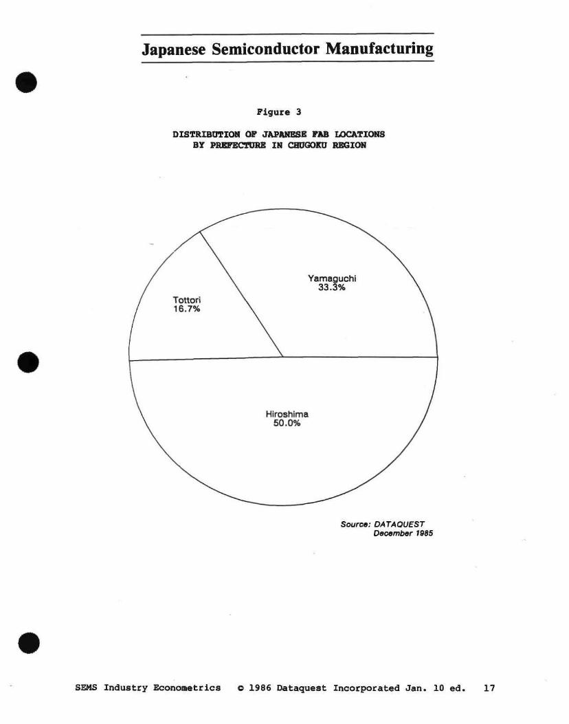
Japanese Semiconductor Manufacturing
F i g u r e 3
DISTRIBOTICm OP JAPJU^SE FJU3 LOCATIONS BY SREFECTDRE IN CflUGOKa REGION
Source: DATAOUEST December 19BS
SEMS Industry Econometrics o 1986 Dataguest Incorporated Jan. 10 ed. 17

Japanese Semiconductor Manufacturing
Figure 4
DISTRIBUTION OF JAPANESE FAB LOCATIONS BY PREFECTURE IN HOKURIKU REGION
Source: DATAOUEST Deoember 1985
18 © 1986 Oataquest Incorporated Jan. 10 ed. SEMS Industry Econometrics

Japanese Semiconductor Manufacturing
Figure 5
DISTRIBUTION OF JAPANESE FAB LOCATIONS BY PREFECTURE IN KANTO REGION
Source: DATAQUEST December 1985
SEMS Industry Econometrics o 1986 Dataquest Incorporated Jan. 10 ed. 19
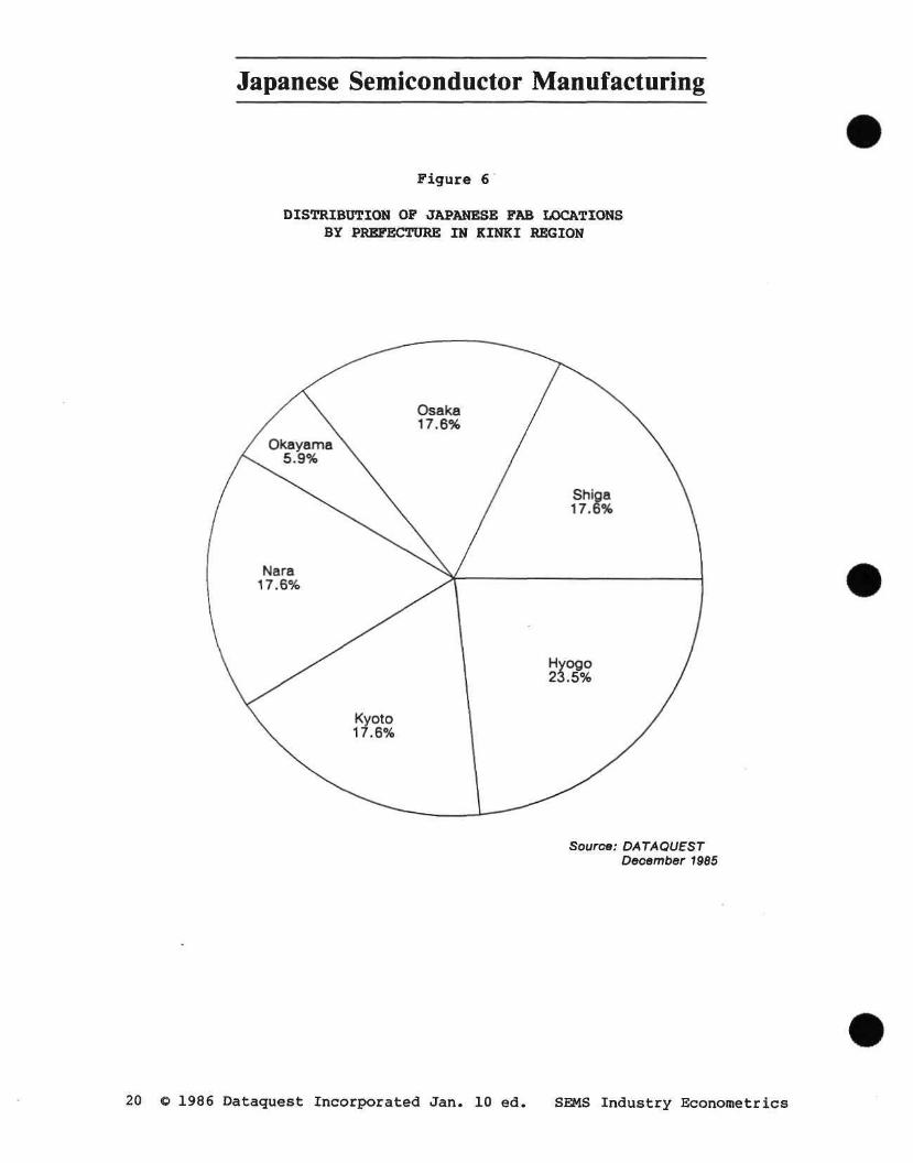
Japanese Semiconductor Manufacturing
Figure 6
DISTRIBUTION OF JAPANESE FAB LOCATIONS BY PREFECTURE IN KINKI REGION
Source: DATAQUEST December 1985
20 © 1986 Dataquest Incorporated Jan. 10 ed. SEMS Industry Econometrics

Japanese Semiconductor Manufacturing
Figure 7.
DISTRIBUTION OF JAPANESE FAB LOCATIONS BY PREFECTURE IN KYUSHU REGION
Source: DATAQUEST December 1965
SEMS Indus t ry Econometr ics © 1986 Dataques t Incorpora ted Jan . 10 ed . 21

Japanese Semiconductor Manufacturing
Figure 8
DISTRIBUTION OF JAPANESE FAB LOCATIONS BY PREFECTURE IN SHIKOKU REGION
Source: DATAQUEST December 1985
22 © 1986 Dataquest Incorporated Jan. 10 ed. SEMS Industry Econometrics

Japanese Semiconductor Manufacturing
•
Figure 9
DISTRIBUTION OF JAPANESE FAB LOCATIONS BY PREFECTURE IN TOHOKU REGION
Source: DATAQUEST December 1985
SEMS Industry Econometrics © 1986 Dataquest Incorporated Jan. 10 ed. 23

Japanese Semiconductor Manufacturing
F i g u r e 10
DISTRIBUTION OF JAPANESE FAB LOCATIONS BY PREFECTURE IN TOKAI REGION
Source: DATAQUEST December 198S
24 © 1986 Dataquest Incorporated Jan. 10 ed. SEMS Industry Econometrics

Japanese Semiconductor Manufacturing
Figure 11
DISTRIBUTION OF JAPANESE FAB LOCATIONS BY PREFECTURE IN TOSAN REGION
Source: DATAQUEST December 1965
SEMS Industry Econometrics © 1986 Dataquest Incorporated Jan. 10 ed. 25

U.S. SEMICONDUCTOR R&D EXPENDITURES— 1987

U.S. Semiconductor R&D Expenditures
Semiconductor research and development is vital for the continued development of new products, applications, and processes. Very few industries are able to match the semiconductor industry's record for R&D expenditures as a percentage of revenue. In the semiconductor industry, R&D expenditures are seed com from which the future emerges.
Table 1 and Figure 1 show U.S. company R&D expenditures. For almost every company in every year, good and bad, R&D expenditures have risen. The compound annual growth rate (CAGR) of R&D expenditures from 1975 to 1988 has been 21 percent.
Table 2 and Figure 2 show U.S. company semiconductor R&D expenditures as a percentage of semiconductor revenue. The general upward trend of this ratio reflects the steady growth and R&D spending for increasingly complex devices and processes. The years when this ratio has turned down are years when revenue has increased sharply; the years when the ratio shows a sharp increase are those in which revenue has fallen.
SEMS Semiconductor Manufacturing © 1989 Dataquest Incorporated January 0003122

U.S. Semiconductor R&D Expenditures
Table 1
U.S. Semiconductor R&D E}q)enditures (Millions of Dollars)
Company
Adaptec Advanced Micro Devices Altera Analog Devices California Micro Devices Chips & Technologies Cypress Harris IDT IMP Intel LSI Logic Linear Technology Micron Technology Motorola National Semiconductor SEEQ Siliconix Silicon Systems Texas Instruments VLSI Technology Xicor ZyMOS
Total
Percent Change
1975
N/A
$ 2 N/A N/A
N/A N/A N/A N/A N/A N/A 13
N/A N/A N/A 44
20 N/A 1
N/A 55
N/A N/A N/A
$135
N/A
1976
N/A
$ 5 N/A N/A
N/A N/A N/A N/A N/A N/A 19
N/A N/A N/A 43
25 N/A
2 N/A 56
N/A N/A N/A
$150
10%
1977
N/A
$ 7 N/A N/A
N/A N/A N/A N/A N/A N/A 25
N/A N/A N/A 49
33 N/A 3
N/A 59
N/A N/A N/A
$175
17%
1978
N/A
$ 10 N/A 3
N/A N/A N/A 6
N/A N/A 37 N/A N/A N/A 60
48 N/A 4
N/A 66
N/A N/A N/A
$234
34%
1979
N/A
$ 24 N/A
5
N/A N/A N/A 9
N/A N/A 60
N/A N/A N/A 75
66 N/A
6 N/A 77 N/A N/A N/A
$321
37%
1980
N/A
$ 33 N/A 7
N/A N/A N/A 13
N/A N/A 89
N/A N/A N/A 92
80 N/A 7
N/A 102 N/A N/A N/A
$423
32%
1981
N/A
$ 42 N/A 8
N/A N/A N/A 16
N/A N/A 109 N/A N/A N/A 116
83 N/A
6 N/A 119 N/A N/A N/A
$500
18%
(Continued)
© 1989 Dataquest Incorporated January SEMS Semiconductor Manufacturing 0003122

U.S. Semiconductor R&D Expenditures
Table 1 (Continued)
U.S. Semiconductor R&D Ejcpendltures (Millions of Dollars)
Company
Adaptec Advanced Micro Devices Altera Analog Devices California Micro Devices Chips St Technologies Cypress Harris IDT IMP Intel LSI Logic Linear Technology Micron Technology Motorola National Semiconductor SEEQ Siliconix Silicon Systems Texas Instruments VLSI Technology Xicor ZyMOS
1982
N/A
$ 63
11
N/A N/A N/A 20 1
N/A 122 2 2 2
128
89 N/A
8 1
128 3
N/A N/A
1983
N/A
$106 0 15
0 N/A
2 22 2 3
132 4 3 1
155
114 5 9 2
163 8 5 4
198*
N/A
$ 169 1 21
1 N/A 5
44 5 3
163 12 2 4
176
158 6 12 3
195 14 8 5
1985
$ 2
207 3 27
1 2 5 47 11 3
175 14 2 5
192
187 6 15 5
214 20 11 4
1986
$ 5 $
223 3 33
1 4 10 36 14 2
178 22 3 4
199
190 7 16 8
256 23 9 4
1987
i 6 $
248 4 56
2 12 19 37 18 7
234 29 4 7
207
213 8 17 9
270 31 8 5
1988
; 7
208 6 61
3 28 32 45 26 8
318 39 5 12 225
255 9 17 12 290 38 10 7
Total
Percent Change
$580 $757 $1,007 $1,159 $1,250 $1,448 $1,661
16% 31% 33% 15% 8% 16% 15%
Note; Columns may not add to totals shown because of rounding. N/A = Not Applicable
Source; Dataquest January 1989
SEMS Semiconductor Manufacturing 0003122
© 1989 Dataquest Incorporated January

U.S. Semiconductor R&D Expenditures
Figure 1
U.S. Company Semiconductor R&D E}q)enditures
Millions of Dollars 1800
1975 1976 1977 1978 1979 1980 1981 1982 1983 1984 1985 1986 1987 1986
0003122-1 Source: DataquMt JanuBfy 19S9
© 1989 Dataquest Incorporated January SEMS Semiconductor Manufacturing 0003122

U.S. Semiconductor R&D Expenditures
Table 2
U.S. Semiconductor R&D Expenditures As a Percentage of Revenue
Company
Adaptec Advanced Micro Devices Altera Analog Devices Califonria Micro Devices Chips & Technology Cypress Harris IDT IMP Intel LSI Logic Linear Technology Micron Technology Motorola National Semiconductor SEEQ Siliconix Silicon Systems Texas Instruments VLSI Technology Xicor ZyMOS
1975
N/A
8% N/A N/A
N/A H/A N/A N/A N/A N/A 10% N/A N/A N/A 13%
4% N/A
5% N/A 11% N/A N/A N/A
197$
N/A
14% N/A N/A
N/A N/A N/A N/A N/A N/A 8%
N/A N/A N/A 10%
6% N/A 8%
N/A 9%
N/A N/A N/A
1977
N/A
8% N/A N/A
N/A N/A N/A N/A N/A N/A 13% N/A N/A N/A 9%
5% N/A 10% N/A 8%
N/A N/A N/A
1979
N/A
8% N/A 6%
N/A N/A N/A 7% N/A N/A 12% N/A N/A N/A 9%
6% N/A 9%
N/A 7% N/A N/A N/A
1979
N/A
12% N/A 8%
N/A N/A N/A 8%
N/A N/A 14% N/A N/A N/A 8%
7% N/A 11% N/A 6%
N/A N/A N/A
1980
N/A
12% N/A 9%
N/A N/A N/A 7% N/A N/A 15% N/A N/A N/A 8%
6% N/A 11% N/A 6%
N/A N/A N/A
1981
N/A
15% N/A 9%
N/A N/A N/A 10% N/A N/A 21% N/A N/A N/A 10%
7% N/A 11% N/A 9%
N/A N/A N/A
Total 9% 8% 8% 8% 8% 8% 10%
(Continued)
SEMS Semiconductor Manufacturing © 1989 Dataquest Incorporated January 0003122

U.S. Semiconductor R&D Expenditures
Table 2 (Continued)
U.S. Semiconductor R&D Expenditures As a Percentage of Revenue
Company
Adaptec Advanced Micro Devices
Altera Analog Devices Califonria Micro Devices
Chips & Technologies Cypress Harris IDT IMP Intel LSI Logic Linear Technology Micron Technology Motorola National Semiconductor SEEQ Siliconix Silicon Systems Texas Instruments VLSI Technology Xicor ZyMOS
1992
N/A
19%. N/A 11%
N/A N/A N/A 13% 45% N/A 20% 38% N/A 40% 11% 8%
N/A 13% N/A 10% 16% N/A N/A
1993
N/A
17% N/A 10%
7% N/A N/A 13% 23% 20% 17% 14% 63% 4% 9% 8%
54% 13% 7% 10% 24% 34% 43%
1984
N/A
15% 467% 10%
8% N/A
123% 17% 15% 10% 14% 14% 14% 3% 8% 8%
11% 12% 5% 8%
20% 21% 22%
1995
9%
26% 70% 12%
8% N/A 29% 19% 21% 11% 17% 10% 13% 15% 10% 13% 20% 14% 10% 12% 25% 34% 24%
19?6
10%
27% 28% 14%
8% 11% 21% 14% 19% 7% 18% 11% 10% 6%
10% 14% 21% 14% 10% 14% 21% 21% 23%
1997
10%
24% 20% 20%
10% 10% 24% 13% 18% 16% 16% 11% 8% 6% 8%
15% 15% 15% 11% 13% 18% 13% 19%
Total 12% 11% 10% 15% 15% 14%
Note: Columns may not add to totals shown because of rounding. N/A = Not Applicable
Source: Dataquest January 1989
© 1989 Dataquest Incorporated January SEMS Semiconductor Manufacturing 0003122

U.S. Semiconductor R&D Expenditures
Figure 2
U.S. Semiconductor R&D Expenditures As a Percentage Revenue
R&D as a Percent of Revenue 18
1975 1976 1977 1978 1979 1S60 1981 1982 19S3 1984 1985 1986 19S7
0003122-2 Source: Dataqueit JFanuary 19S9
SEMS Semiconductor Manufacturing 0003122
© 1989 Dataquest Incorporated January