Benchmarking Semiconductor Lithography Equipment ...
86
Benchmarking Semiconductor Lithography Equipment Development & Sourcing Practices Among Leading-Edge U.S. Manufacturers by Charles N. Pieczulewski B.S. Materials Science & Engineering, Northwestern University (1992) Submitted to the Department of Materials Scienceand Engineering in Partial Fulfillment of the Requirements for the Degrees of Master of Science in Materials Science and Engineering and Master of Science in Technology and Policy at the MASSACHUSETTS INSTITUTE OF TECHNOLOGY June 1995 © Charles N. Pieczulewski 1995. All rights reserved The author hereby grants to MIT permission to reproduce and to distribute publicly copies of this thesis document in whole or in part. Signature ofAuthor Certified by Certified by Accepted by Accepted by MASSACHUSETTS INSTITUTE OF TECHNOLOGY C\ THA I ;-T I May 12, 1995 Professor Charles H. Fine / A Thesis Supervisor Professor Joel Clark ialsScience and Engineering chnolpgv and Policy Program Pf4ssor Richarae Neufville Chairman, Technology and PolicyProgram Cal V. Thompson II Professor of Electronic Materials Chair, Departmental Committee on Graduate Students JUL 201995 -1- LIBRARIES as
Transcript of Benchmarking Semiconductor Lithography Equipment ...
Benchmarking Semiconductor LithographyEquipment Development & Sourcing Practices
Among Leading-Edge U.S. Manufacturers
by
Charles N. Pieczulewski
B.S. Materials Science & Engineering,Northwestern University (1992)
Submitted to the Department of Materials Science and Engineeringin Partial Fulfillment of the Requirements for the Degrees of
Master of Science in Materials Science and Engineeringand
Master of Science in Technology and Policy
at theMASSACHUSETTS INSTITUTE OF TECHNOLOGY
June 1995
© Charles N. Pieczulewski 1995. All rights reservedThe author hereby grants to MIT permission to reproduce and to
distribute publicly copies of this thesis document in whole or in part.
Signature of Author
Certified by
Certified by
Accepted by
Accepted by
MASSACHUSETTS INSTITUTEOF TECHNOLOGY
C\ THA I ;-T I May 12, 1995
Professor Charles H. Fine/ A Thesis Supervisor
Professor Joel ClarkialsScience and Engineeringchnolpgv and Policy Program
Pf4ssor Richarae NeufvilleChairman, Technology and Policy Program
Cal V. Thompson IIProfessor of Electronic Materials
Chair, Departmental Committee on Graduate Students
JUL 201995-1-LIBRARIES as
Benchmarking Semiconductor LithographyEquipment Development & Sourcing Practices
Among Leading-Edge U.S. Manufacturers
Charles N. Pieczulewski
ABSTRACT
The semiconductor lithography equipment industry has evolved towhere knowledge of technology alone is insufficient to survive in themarket. An interdisciplinary set of skills has become necessary to fullycomprehend the dynamics of the lithography industry. Understandingthe fundamental technology, the management issues in amanufacturing equipment market, and the role of industry-sponsoredconsortia are all critically important to the lithography industry.
A dramatic shift in the semiconductor lithography equipmentmarket occurred in the mid-1980s which sparked a furry amongpolitical circles in the United States. Between the late 1970s and late1980s the market share of U.S. companies dropped from nearly 90% toless than 20%. The rapid expansion of the semiconductor market,particularly in Japan, coupled with the perceived unresponsiveness ofU.S. lithography suppliers to customer requests provided a window ofopportunity for Nikon and Canon. In addition, the technologicalexpertise necessary to manufacture lithography equipmentincreasingly forced semiconductor manufacturers world-wide topurchase the equipment from suppliers rather than to developinternally.
In the 1990s, U.S. semiconductor manufacturers have adapted to thenew market conditions for lithography equipment sourcing.Lithography technology remains critical to the semiconductormanufacturing process. Constrained to buy lithography equipmentfrom suppliers, manufacturers are forced to develop strategies foreffective technology supply chain management. Driven by technologydevelopment cycles, semiconductor companies have a four year timeconstant for learning and continuously improving their sourcingstrategy. As a result of their dependency upon suppliers,semiconductor corporate equipment sourcing strategies have beengeared to maximize supplier switching flexibility while simultaneouslyminimizing capital expenditures. This approach has lead manymanufacturers to create preferred supplier relationships and tools forensuring competitive behavior among suppliers. The industry'sobjective: to ensure continuous development of leading-edgelithography technology. This report benchmarks how individualcompanies have organized their equipment development and sourcingpractices and their respective merits.
Thesis Supervisor: Professor Charles H. Fine, Sloan School of ManagementThesis Advisor: Professor Joel Clark, Dept. Materials Science and Engineering
-2-
Benchmarking Semiconductor LithographyEquipment Development & Sourcing Practices
Among Leading-Edge U.S. Manufacturers
Table of Contents
ABSTRACT 2
Table of Contents 3List of Tables & Figures 5Acknowledgements 6
1 The Art of Managing ManufacturingEquipment Development & Sourcing 7
1.1. Thesis Research Objectives 8
1.2. Lithography Research Design Tools 9
2 A Political Economist's Perspective 14on Japan's Entrance into theSemiconductor Equipment Market
2.1. The Hype and Mystique of 16Japan's Emergence
2.2. The Timely Research Association: 21Japan's VLSI Project
2.3. Decade of Changing Tides in the 36Lithography Market
-3-
Table of Contents
3 Corporate Equipment SourcingStrategies to Minimize CapitalExpenditures while MaximizingSupplier Switching Flexibility 39
3.1. Equipment Criticality: Lithography as theCompetitive Technology Driver of theSemiconductor Industry 40
3.2. The Make-Buy Spectrum: Industry Focus onSupply Chain Management 50
3.3. Cyclicality: The Industry-wide EquipmentSourcing Cycle 53
3.4. Interdependence & Dependency AmongSemiconductor Manufacturers 57
3.5. Internal Corporate Equipment SourcingStrategies 66
3.6. Supplier Relations & Equipment Evaluation:The 7 Steps to Lithography EquipmentSourcing 74
3.7. Opportunities for Further Learning inCreating and Managing SemiconductorTechnology Supply Chains 77
4 APPENDIX 79
4.1. Seminar Presentation Slides 80
4.2. Sample Questions from Corporate Survey 85
-4-
TABLES
2.1
3.1
3.2
3.3
3.4
3.5
List of Tables & Figures
DESCRIPTION
Top 5 Ranking Lithography Equipment SuppliersWorld-Wide Market Share
Top-Ten Merchant Semiconductor Manufacturers(1994)
Top-Ten Merchant Capital Spenders (1994)
Internal Mask Strategies Among Six Leading-EdgeCompanies
Six Perspectives on the Three Spheres
Top 5 Semiconductor Equipment Selection Criteria
PAGE
18
46
47
61
67
77
FIGURES DESCRIPTION PAGE
1.1 The 7 Benefits to Corporate Participation 12
2.1 Global Lithography Equipment Market SharePercentages by Supplier Origin 18
3.1 Lithography Technology Nodes for PentiumrmProcessor Generations 42
3.2 Illustration of die size shrinkage relationship to numberof chips per silicon wafer 44
3.3 Worldwide Lithography Stepper 1993 Market Shares 49
3.4 Make-Buy Spectrum 52
3.5 Worldwide Lithography Equipment Sales (1978-1994) 54
3.6 Stages of Internal Technology Development for VolumeManufacturing 56
3.7 Capability Learning Dependency Loop 58
3.8 Three Spheres in the Semiconductor Realm 66
3.9 Centralization - Decentralized Equipment Sourcing 68
3.10 Vanilla 7 Step Equipment Sourcing 76
-5-
----
Acknowledgements
It is hoped reading this text will bring you as much enjoyment and knowledgeas it did for author during the research process. This research is part of anMIT project on technology supply chains direct by Professor Charles H. Fine.
As always, an effort such as this could not have been possible without theguidance and support from my family, friends, and colleagues. I am in debt toProfessor Charles H. Fine, whose guidance, support, and patience as mythesis supervisor provided this unique opportunity to create aninterdisciplinary thesis research project.
I am grateful to the lithography managers among the participating companies:Advanced Micro Devices (AMD), Digital Equipment Corp. (DEC), IBM Corp.,Intel Corp., Motorola Inc., and Texas Instruments Inc. for their cooperationand willingness to learn more about managing their own technology supplychain. Research funding support from the MIT Leaders for Manufacturing(LFM) Research Program, MIT-Japan Program, and MIT Center forInternational Studies has been essential to make this dream become reality.
For those who have taught me so much along the way, I send my regards to amentor who introduced me to an entirely new way to look at the world. I amgrateful for the opportunity to have University of Tsukuba, Japan, ProfessorShoji Shiba introduce me to the concepts and tools which have facilitated myefforts in managing total quality in everything I do. Many thanks also to MITVisiting Professor Ronald Dore, his extensive knowledge and teachings of the"Political Economy of Japanese Organizations" provided an enlightedperspective on doing business in Japan. And sincere gratitudes to SachikoSuzuki, whose charm provided me with the determination to efficiently surveysemiconductor organizations in Texas and whose inspiration carried methrough those laborious weeks of thesis composition.
-6-

Chapter
The Art Of Managing Manufacturing EquipmentDevelopment & Sourcing
-7-
1.1. Thesis Research Objectives
The MIT Technology Supply Chains Research Group
This research is part of a larger MIT project on technology supply chains
direct by Professor Charles H. Fine. The MIT project seeks to characterize
the equipment development and sourcing practices across multiple industries.The underlying hypotheses driving this research program have been the
foundation of this project on semiconductor lithography equipment technology
supply chains.
The S.M. Lithography Thesis Objectives
The vision is to expand the academic knowledge-base and provide the
framework for semiconductor manufacture's and their equipment suppliers toseek optimal strategies in the management of lithography technology
development and sourcing. This vision is built upon seven specific objectives:
1. To integrate an international database on semiconductor lithographyequipment development and sourcing proactices, compile an interpretationof lithography industry trends, and recommen metrics for benchmarkingmanufacturing equipment development and sourcing activities.
2. To map-out a dynamic model of users, suppliers, end-product customers,and government involvement in the lithography industry.
3. To develop an understanding of the critical links along the lithographytechnology supply chain.
4. To identify benchmark technology development and sourcing processeswhich are to the mutual advantage of both users and suppliers oflithography equipment.
5. To explore the true end-product customer-driven technology pull foradvancing lithography to progressively smaller linewidths.
6. To develop case studies of lithography equipment development and sourcingprocesses within and between equipment users and their suppliers.
-8-

7. To clarify the details concerning current and future government policies insupport of lithography equipment technology.
A key source of data in fulfilling these objectives was to directly ask
lithography technology managers working in semiconductor manufacturingcompanies. Literature research only reveals the technical aspects of
lithography. To learn how the industry functions and its daily managementchallenges required fieldwork. Eventually, through this thesis project the
"Lithography Technology & Policy Story" which others can locate via
literature research can become available.
1.2. Lithography Thesis Research Design Tools
Three core research tools were developed to collect data from six
semiconductor manufacturing companies and the Sematech researchconsortia:
1. The 7 Step Corporate Management Survey Approach,
2. The 7 Lithography ED&S Questionnaires, and
3. Three Tools for Encouraging Corporate Participation.
Nineteen of 21 interviews with lithography managers were recorded on
audio tape to supplement written notes. On average, each of the six
companies required a minimum of three interviews to capture sufficient
information from each company. An early sampling of five independent
interviews with Texas Instruments indicated the first three intervieweesanswered 80%+ of all desired questions (Consult 80/20 Rule).
The 7 Step Corporate Management Survey Process
From the thesis' inception it was realized the need for a methodological
process to survey the semiconductor industry's lithography equipmentdevelopment and sourcing practices. In the end six U.S. Semiconductor
-9-
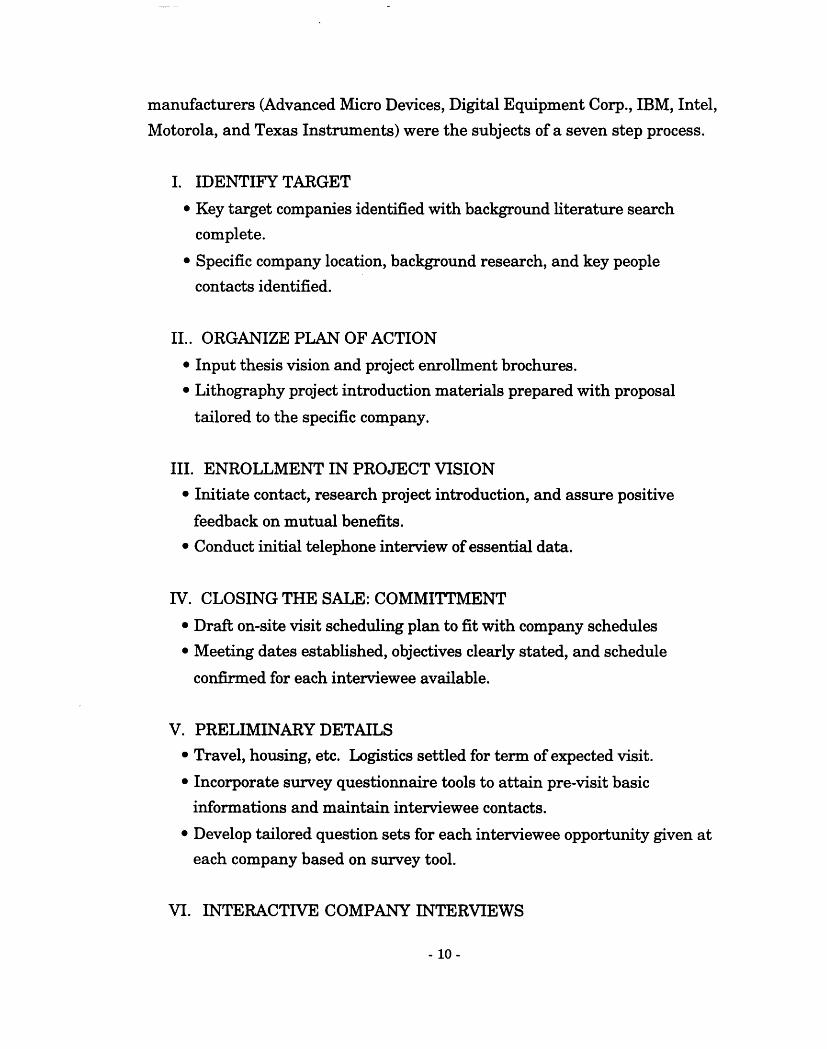
manufacturers (Advanced Micro Devices, Digital Equipment Corp., IBM, Intel,
Motorola, and Texas Instruments) were the subjects of a seven step process.
I. IDENTIFY TARGET
* Key target companies identified with background literature search
complete.
* Specific company location, background research, and key people
contacts identified.
II.. ORGANIZE PLAN OF ACTION
* Input thesis vision and project enrollment brochures.* Lithography project introduction materials prepared with proposal
tailored to the specific company.
III. ENROLLMENT IN PROJECT VISION
* Initiate contact, research project introduction, and assure positive
feedback on mutual benefits.
* Conduct initial telephone interview of essential data.
IV. CLOSING THE SALE: COMMITTMENT
* Draft on-site visit scheduling plan to fit with company schedules* Meeting dates established, objectives clearly stated, and schedule
confirmed for each interviewee available.
V. PRELIMINARY DETAILS
* Travel, housing, etc. Logistics settled for term of expected visit.
* Incorporate survey questionnaire tools to attain pre-visit basicinformations and maintain interviewee contacts.
* Develop tailored question sets for each interviewee opportunity given ateach company based on survey tool.
VI. INTERACTIVE COMPANY INTERVIEWS
- 10-

* Conduct on-site interviews at company
* Ensure full data collection, interview notes and recordings.
VII. POST-INTERVIEW REPORTS AND FEEDBACK
* Short-term response: thank you notes and initial overview of researchdata collected.
* Author final case-study report for each company to confirm data.
Three Tools For Encouraging Corporate Participation
The critical success factor to the "Corporate Management Survey Process"
was step III. Enrollment in Project Vision. Fundamentally, it was quickly
learned that managers wanted to know what were the benefits to them, how
much time would it take, and what specific information we wanted to learn
from them. Hence, three tools were developed to help in this process of
enrolling each semiconductor company's interest in participating:
1. The 7 Benefits to Corporate Participation
2. Details in the Research Process
3. Introductory Questionnaire
Introducing the research project and expectations also had to be straight-forward to the participant. A key diagram used to introduce "The 7 Benefits to
Corporate Participation" as in Figure 1.1.
- 11-
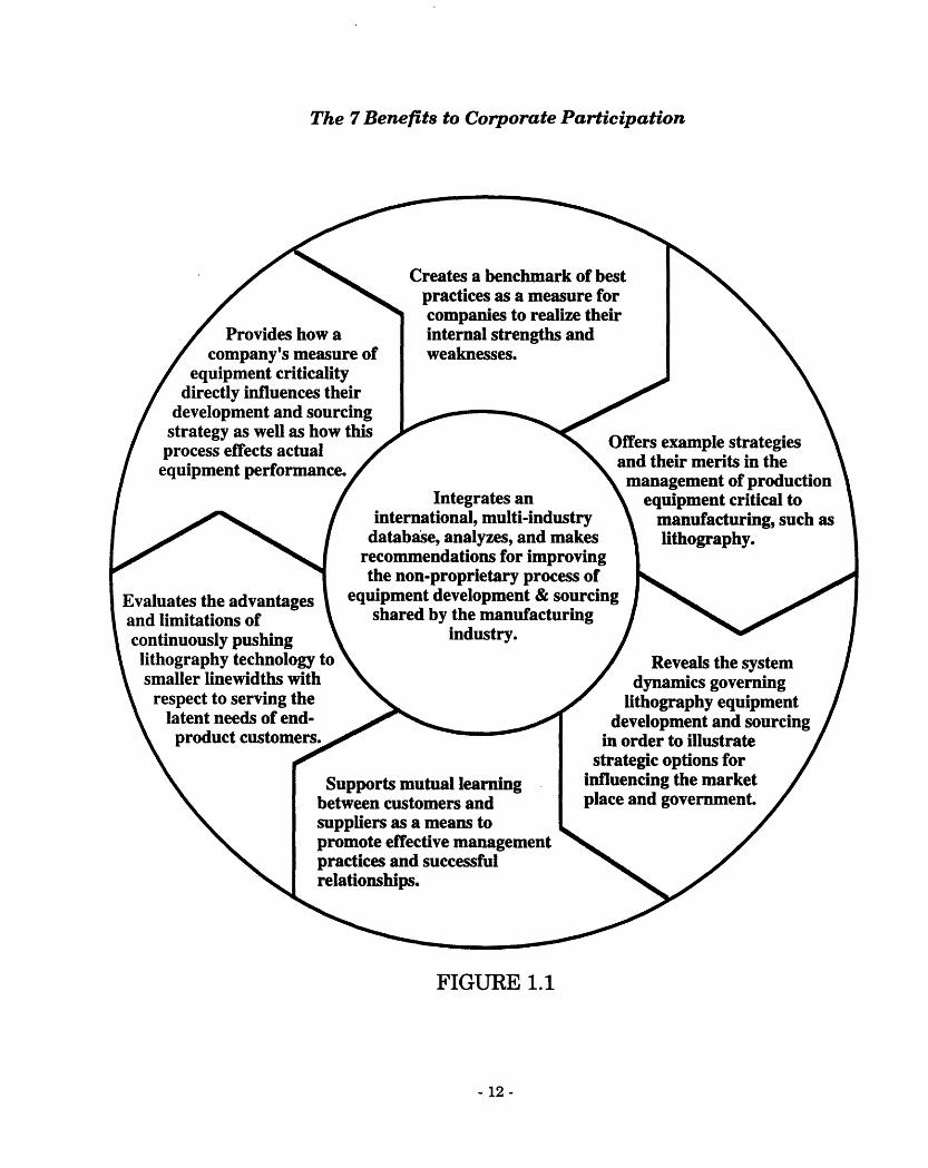
The 7 Benefits to Corporate Participation
Creatpra
/ conProvides how a int
company's measure of wetequipment criticality
directly influences theirdevelopment and sourcingstrategy as well as how thisprocess effects actualequipment performance.
IniI internatioi
database, arecommend:the non-pr(
Evaluates the advantages equipment deand limitations of shared bycontinuously pushing ilithography technology to\ smaller linewidths with
respect to serving thelatent needs of end-product customers.
N
Supports mutualL -,& ..... ...
Ies a benchmark of bestctices as a measure fornpanies to realize theirernal strengths andaknesses.
Offers example strategiesand their merits in themanagement of production
tegrates an \ equipment critical torial, multi-industry manufacturing, such asmalyzes, and makes lithography.ations for improving)prietary process ofvelopment & sourcingthe manufacturingindustry.
Reveals the systemdynamics governing
lithography equipment
I learning....
etween customers anasuppliers as a means topromote effective managempractices and successfulrelationships.
development and sourcingin order to illustrate
strategic options forinfluencing the marketplace and government.
ient
FIGURE 1.1
- 12-
--
- - -
i/
N I
-
, \
tegrates an equipment critical torial, multi-industry manufacturing_, such asanalyzes, and makes lithography.ations for improving)prietary process ofvelopment & sourcingthe inanufacturi gindustry.
Reveals the systemdynamics governing
lithography equipment
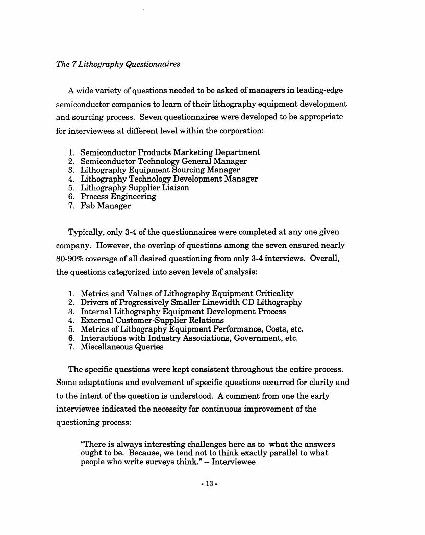
The 7 Lithography Questionnaires
A wide variety of questions needed to be asked of managers in leading-edge
semiconductor companies to learn of their lithography equipment development
and sourcing process. Seven questionnaires were developed to be appropriate
for interviewees at different level within the corporation:
1. Semiconductor Products Marketing Department2. Semiconductor Technology General Manager3. Lithography Equipment Sourcing Manager4. Lithography Technology Development Manager5. Lithography Supplier Liaison6. Process Engineering7. Fab Manager
Typically, only 3-4 of the questionnaires were completed at any one given
company. However, the overlap of questions among the seven ensured nearly
80-90% coverage of all desired questioning from only 3-4 interviews. Overall,
the questions categorized into seven levels of analysis:
1. Metrics and Values of Lithography Equipment Criticality2. Drivers of Progressively Smaller Linewidth CD Lithography3. Internal Lithography Equipment Development Process4. External Customer-Supplier Relations5. Metrics of Lithography Equipment Performance, Costs, etc.6. Interactions with Industry Associations, Government, etc.7. Miscellaneous Queries
The specific questions were kept consistent throughout the entire process.
Some adaptations and evolvement of specific questions occurred for clarity and
to the intent of the question is understood. A comment from one the early
interviewee indicated the necessity for continuous improvement of the
questioning process:
"There is always interesting challenges here as to what the answersought to be. Because, we tend not to think exactly parallel to whatpeople who write surveys think." -- Interviewee
- 13-

Chapter 2
A Political Economist's Perspective on Japan's Entranceinto the Semiconductor Equipment Market
- 14-
Nippon Kogaku K.K and Canon Inc.'s Entrance and Subsequent Dominance inthe Lithography Equipment Market, 1975-1995.
ABSTRACT
A dramatic shift in the semiconductor lithography equipment marketoccurred in the mid-1980s which sparked a furry among political circles in theUnited States. What was once a lithography equipment market which was90% U.S.-based in the late-1970s became less than 20% by the late 1980s. Inthe early 1990s, roughly 86% of lithography equipment is produced by three
Japanese manufacturers: Nikon, Canon, and Hitachi.These Japanese suppliers happened to be manufacturing a product in
which incremental process improvements, refined technology, and impeccablecustomer service, the hallmarks of Japanese corporate culture, were keyelements to success. Accelerated by timely, indirect participation in the MITIorchestrated VLSI Technology Research Association, Nikon and Canon had
core technical competencies which positioned them very competitively toenter the lithography equipment market. Despite some politically-chargedviews in the West, Nikon and Canon's success in the marketplace is not about'Japan Inc.' targeting lithography technology or any concerted Japanese effortto keep-out foreign competition.
The rapid expansion of the semiconductor market, particularly in Japan,coupled with perceived unresponsiveness of U.S. lithography suppliers tocustomer requests provided a window of opportunity for Nikon and Canon. In
addition, the technical expertise necessary to manufacture lithographyequipment increasingly forced semiconductor manufacturers worldwide to out-
source the equipment and further opened the market to suppliers during the1980s.
Lessons from the VLSI Project and the ever-present trade friction with theU.S. has significantly influenced the nature of MITI's modern engineering
research associations in Japan, as exemplified by the Super Silicon CrystalProject. Korea is attempting to emulate Japan's approach. However, whether
Japan is an appropriate role model to emulate is questionable.
- 15-

2.1. THE HYPE AND MYSTIQUE OF JAPAN'S EMERGENCE
The Market Power Shift of the Lithography Equipment Industry
If semiconductors are the "crude oil" of the second industrial revolution,
then the fantastically precise machines that make microchips are the drillingrigs of the information age.1 As the machines which essentially pattern the
circuit designs of 100+ chips per minute with accuracy's to dimensions on the
submicron (10-6 m) scale, lithography equipment can be characterized as the
workhorse of the industry. Ever since the marketing of 64 kilobit (Kb) dynamic
random access memory (DRAM) chips in the early 1980s successive,
incremental advances in lithography technology has paced each generation of
semiconductor technology (from 64 Kb, 256 Kb, 1 Mb, 4 Mb, to the 64 Mb
DRAMs in production today).
In the mid-1970s the dominant players in the lithography equipment
business were the U.S. suppliers Perkin-Elmer Corporation and GCA.2 For
most the decade these two firms led their competitors with their respective
lithography technologies. Canon entered the lithography (wafer exposure)
business in 1979 with an automated version of the proximity aligner, a
technology that Perkin-Elmer had made obsolete with a more advancedprojection aligner technology introduced back in 1973. However, Canon's
machine represented such a great improvement over previous products of itstype that it enabled many semiconductor manufacturers to use it instead of
the more expensive projection aligner (of Perkin-Elmer's) or stepper aligner
technology of GCA.3
1 Business Week "The New Japanese challenge in chipmaking," April 18, 1983 p.114B.
2 Geophysics Corporation of America (GCA).
3 Global Competitiveness of U.S. Advanced Technology Manufacturing Industries:Semiconductor Manufacturing and Testing Equipment, Report to the Committee onFinance, United States Senate, Investigation No. 332-303 Under Section 332(g) of theTariff Act of 1930, USITC Publication 2434, Washington D.C. September 1991 p.4 -9.
- 16-

Later in 1981, Nippon Kogaku K.K.4 entered the market with its firstproduct extremely competitive with GCA's stepping aligner lithography
technology. It was quite clear by the early 1980s that stepping aligners was to
be a superior and preferred technology for the most advanced, smallest circuit
design patterns, however it came at a significant cost in manufacturing
throughput compared to the proximity/projection aligners. During this period
either of the lithography technologies were competitive in the market,depending upon the type of application for the equipment used by
semiconductor manufacturers.However, over the course of the 1980s there was a clear shift in the market
share powers in lithographic equipment. From 1982 to 1989 world sales of
lithography (and associated) equipment nearly tripled, from $415 million to
$1.2 billion, but the sales by U.S. companies declined from $240 million to $215
million, and their market share dropped from 62% to 21%. Over the same time
period, the market share of Japanese companies nearly doubled from 38% to
70% and their sales rose by a factor of nearly six, Figure 2.1. GCA and Perkin-
Elmer Corp., the U.S. suppliers that dominated the market at the beginning ofthe 1980s, lost their leadership position to Nikon and Canon of Japan.5 See
Table 2.1. The turning point occurred, coincidentally, in 1985 when Nikon and
GCA virtually split the world market share as suppliers for the then dominant
stepping lithography equipment.6
4 Nikon is formally named Nippon Kogaku K.K.. It's common nameplate is Nikon and itsU.S. Subsidiary is named Nikon Precision, Ltd.
5 Global Competitiveness . . Prev.cited.6 The Japan Economic Journal, July 2, 1985 p.17.
- 17-
Global Lithography Equipment Market SharePercentages by Supplier Origin
1982
Europe
9%
Japan
38%
U.S.
62%
Japan
70%
Source: VLSI Research, Inc.7
FIGURE 2.1
Top 5 Ranking Lithography Equipment SuppliersWorld-Wide Market Share
* SVGL was formerly Perkin-Elmer
TABLE 2.1
7 Global Competitiveness . . .,Prev.cited.
- 18-
1989
U.S.
21%
1982 MarketShare
#1 Perkin-Elmer (U.S.) 32.6%
#2 Canon (Japan) 15.8%
#3 Nikon (Japan) 13.5%
#4 GCA (U.S.) 10.4%
#5 Eaton (U.S.) 5.6%
1989 MarketShare
#1 Nikon (Japan) 37.9%
#2 Canon (Japan) 24.1%
#3 GCA (U.S.) 9.3%
#4 ASML (Neth.) 8.8%
#5 SVGL *(U.S.) 5.8%
Hype, Fear, & Rage within U.S. Political Circles
The clear shift in market leadership of lithography technology was quickly
identified as another story in the legacy of losing a vital sectors of U.S.-born
technology to the Japanese. Then it became an issue of U.S. national security.During the heights of the cold war, semiconductor technology provided the
technological basis for America's qualitative lead in nuclear missiles, precision
guided munitions, cruise missiles, surveillance and early warning systems,
communications, aircraft, and an assortment of conventional weaponry. 8 The
concerns were both of military and economic security. What if, for example,
Japanese corporations develop state-of-the-art equipment, would they sell itwithin the Soviet-bloc? Will they sell such equipment to their competitors in
the U.S.? Or will they withhold them? Will the experience gained in equipment
manufacturing give them any extra edge in production know-how?
Of course, it wasn't only in the lithography equipment industry were U.S.semiconductor equipment suppliers were being confronted by the competitive
Japanese. The hype played up within U.S. political circles lend to supporting
government investments into GCA to help them survive in the lithography
market and, ultimately, the formation of the U.S. semiconductor customersupplier consortia Sematech in 1988.
However, many fear that money alone will not revive the U.S.
semiconductor equipment industry. Robert Graham, CEO of Novellus
Systems Inc. believes, "There is enough money in the industry. What it lacks
is good management." 9 The truths to Mr. Graham's message becomes quite
evident when one delves deeper into the woes of America's lithography
equipment industry.
8 Okimoto, Daniel I., et.al., Competitive Edge: The Semiconductor Industry in the U.S.and Japan (Stanford University Press: Stanford, CA) 1984 p.3.
9 Electronic Business "Semi equipment makers: partner or perish," vol.17, no.10, May 20,1991 p.34.
- 19-

Hype, Fear, & Economic Planning within Japanese Political Circles
Not without coincidence, it was by equally prevalent hype and realistic fear
which drove the Ministry of International Trade and Industry (MITI) to have
major headaches about the economic viability of Japan's semiconductorindustry. By its wide range of product applications, semiconductor technology
is absolutely essential to a spectrum of industries: telecommunications,
computers, machine tools, avionics, consumer electronics, and robotics, to
name a few. In addition, the rumor that IBM was on its way to launching a
one-chip-computer became a rallying force within political circles in Japan and
the reference was often made to Commodore Perry's black ships which in 1853
forced Japan to completely change its relations with the outside world. 10
Significant figures within Japan's ruling Liberal Democratic Party (LDP) andMITI made it very clear that to leave the potentially huge Japanese computer
industry to the vagaries of the free market would be unwise in the long run.
Japan would ultimately be a nation hostage to IBM's technological whims and
would hinder Japanese companies' abilities to compete in related technology
products, as mentioned.1 1
"We have too many computer makers in Japan to cope with the monster,IBM," said Tomisaburo Hashimoto, a leader of the LDP in 1975, "the
reorganization of the computer industry and the establishment of a moreunified and more integrated development organization for VLSI technology are
urgently needed."12
Henceforth, MITI was pressured by the LDP to build support among
10 Sigurdson, Jon Industry and State Partnership in Japan: The Very Large Scale
Integrated Circuits (VLSI) Project (Tryckericentralen AVC: Lund, Sweden) Research
Policy Institute, Univeristy of Lund, Sweden 1986 p.61 .
11 Anchodoguy, Marie Computer Inc.: Japan's Challenge to IBM (Harvard University Press:
Cambridge, MA) 1989 p.3.
12 Nikkan Kogyo Shinbun, Tokyo, May 7, 1975 (translation from original).
- 20 -

industry to form a Very Large Scale Integrated (VLSI) Technology Research
Association out of the necessity to match IBM's next-generation computer
technology. In Japan, IBM was expected then to introduce the "one-chip
computer" at the latest by 1980. Therefore, the target technology and time
limit was clear from the beginning for MITI and the LDP.13 As credence to
this view, U.S. Federal Bureau of Investigations (FBI) undercover operations
disclosed the IBM Spy Incident (IBM supai jiken) indicting Hitachi for secret
missions in search of IBM computer technology. 14
Hype and fear of IBM led MITI down a path of an attempt at economic
planning and resulted in the now famous VLSI Project.
2.2. THE TIMELY RESEARCH ASSOCIATION:JAPAN'S VLSI PROJECT
The Birth of Engineering Research Associations in Japan
The British research associations of the 1960s and 70s served as an
inspiration and role model in certain aspects of Japan's similar policyinstrument - the engineering research association (kogaku kogyo gijitsu
kenkyu kumiai). The father of Japan's evolving engineering researchassociations (ERA) was a Dr. Masao Sugimoto, director of the Mechanical
Engineering Laboratory (MEL, 1953). Dr. Sugimoto had the opportunity to
tour facilities in the U.K. during his tenure at MEL and was instrumental in the
formation the first ERA to improve automotive radiator technology in 1955.15
However, Japan's engineering research associations evolved to be much
13 Sakakibara, Kiyonori From Imitation to Innovation: The Very Large Scale Integrated
(VLSI) Semiconductor Project in JapanAlfred P. Sloan School of Management Working
Paper 1490-83 (M.I.T.: Cambridge, MA) October 1983 p.1 6.
14 Anchordoguy, prev.cited.
15 Sigurdson, p.12.
- 21 -
different that the U.K. role model. Law providing the means for government
involvement and setting limits to engineering research associations in Japan
were formulated in 1961. Most notable early example was the camera
association created soon thereafter in 1962. At the time many of the
organizational ideas were borrowed from the Scientific Instrument Research
Association (SIRA) in the U.K. The differences in the structure of the
Japanese ERA system was two-fold:
1. Company membership was generally on average 12-17 companies
during the 1960s and 70s.
2. None of the ERAs in Japan were permanent organization and rarelylasted more than six years.16
Initially the camera association did not have its own research laboratory
and the research was done at universities and in member companies. AJapan's camera technology had in 1955 already reached the level of
manufacturers in West Germany and it was necessary to move into newtechnological fields. There was a realized need for the camera makers to
introduce the use of electronics and plastics in order to compete more
efficiently in the world market. Overall, the camera association provided the
technological basis for continuous improvement for the manufacture of
cameras and is seen as an outstanding success. Member companies naturally
included Nippon Kogaku K.K. (Nikon), Canon, Olympus, Konishiroku (Konica),
Fuji Films and others. 17
16 Sigurdson, p.23.
17 Sigurdson, p.20-22.
- 22 -
MITI clarified that engineering research associations had four main
benefits to Japan:
1. Risk-sharing and cost-sharing between participating units
2. Pooling of resources to speed-up the research process and eliminate
overlap
3. A comprehensive research approach which means that resources
are pooled both horizontally and vertically through to marketable
products4. Exchange of information which raises the technological level through
the relevant system of an industrial sector.
Since the enactment of the engineering research association law in Japan
some thirty ERAs had been established up until 1976. These ERAs included
everything from automotive components, cameras, to electric power systems.
Then came the Very Large Scale Integrated (VLSI) Technology Research
Association (code named the VLSI Project).
Struggles in the Formation & Organization of the VLSI Project
At the onset Japanese companies were unhappy with the assertions that
they couldn't be competitive in the world market. The rivals Hitachi, Fujitsu,
Toshiba, Mitsubishi and NEC were clearly from different roots and competitive
groups within Japan. MITI was also skeptical of the results of a massive joint
effort aimed at developing VLSI technology and anticipated strong resistance
from the semiconductor companies. However the political powers within the
LDP persisted. 18 Although with much grumbling, all five companies agreed
they could not help but to follow the "bureaucrat's blueprint" if they were to get
- 23 -
18 Sakakibara, p.4.
any government subsidies.19 Cases of such allegiance to cooperate with
government authority by the Japanese dates back to an era of Workmen's
Guilds during the Tokugawa Period.20
Thus, during the four year project, an average of ¥17.5 billion ($72 million)21
was invested annually, roughly 50% of which came from MITI. Ironically,
nearly a quarter to a third of the projects money was spent in the U.S. to
purchase the most advanced semiconductor manufacturing and testequipment from U.S. suppliers.22 It is important to keep in mind, however,
that annual research expenditures on the order of $72 million is not anoverwhelmingly large amount. Leading U.S. semiconductor manufacturer's
R&D spending independently in 1977 was $96 million by Texas Instruments,
$110 million by Motorola, and $44 million by Fairchild Camera & Instrument,
for example. 23
Once the VLSI Project was established, the unrest between companies in
the association still prevailed. The first year was a tough time for thecompanies to negotiate where the cooperative research laboratory would be
located and agreeing upon what research the consortia would do jointly. It is
important to note that the Japanese social imagery of working harmoniously
together and avoiding confrontation does not apply in this case. The strict
social hierarchy was lost once researchers stepped out of their home
companies and had to negotiate with competitors in the market.The VLSI project's first chairman of the board was Hitachi's president,
19 Asahi Shinbun, Tokyo, July 16, 1975 (translation from original).
20 Takekoshi, Yosoburo The Economic Aspects of the History of the Civilization of Japan
(MacMillan Co.: New York) vol.3, 1980 p.2 42.
21 At the 1975 exchange rate of Y243 = $1.
22 Sakakibara, p.14.
23 Business Week July 3, 1978 p. 7 6 .
- 24 -

Hirokichi Yoshiyama and the managing director was a retired MITIbureaucrat, Masato Nebashi, who had much experience in managing national
projects as an executive official.24 Nebashi's appointment is exemplary of the
Japanese system of amakudari, "decent from heaven." Some 300
bureaucrats annually join the ranks of the business world as directors or senioradvisors of corporations they monitored during their government career, most
typically from within the Japanese ministries.25Eventually the 100 researchers brought together under one roof developed
a sense of cohesion and began to make significant research advances. The
leadership of Mr. Nebashi has been frequently cited as playing a critical role in
helping the researchers to communicate and function as a group'What I did was the typical Japanese way: All I did for this four years was
to drink with them as frequently as I could. I wanted to understand their
complaints on those occasions and tried to eliminate problems," says
Nebashi.2 6 Researchers characterized Nebashi's leadership as traditional"management by whisky."
The Intangible, Unexpected Results of the VLSI Project
If the objective of the VLSI Project was to be capable of building a one-chip
computer like IBM by 1980 then the project failed miserably. Although, it is
important to keep in mind that, even to this very day in 1994, neither IBM nor
any other company has built a one-chip computer. However, if the objectivewas for these Japanese companies to understand and develop state-of-the-art
semiconductor process technology to manufacture the ultimate one-chip
24 Sakakibara, p.22.
25 Van Wolferen, K. The Enigma of Japanese Power (Knopf: New York) 1989 p.45.
26 Nebashi, Masato "VLSI kaihatsu - kyogo gosha ni yoru kyodo project no yonen kan
(Developing VLSI -A four year project of competitive firms)" Management, Tokyo,
November 1980, p.60 . Reprinted in Sakakibara.
- 25 -

computer, should it ever be designed, then the VLSI Project was an
extraordinary success.
It was clearly decided during the first year of the VLSI Project that circuitdesign development would not be included in the joint effort and each company
eventually established independent pilot production lines. As a result much ofthe effort taken by the consortia concerned improving manufacturing
processes. 27 The expertise of Japan's zaibatsu groups in absorbing new
technology and refining manufacturing techniques has been Japan's forte ever
since the ship engine yards of Pre-World War II.28
Six research teams eventually evolved within the VLSI Project and included
MITI's Electro-Technical Laboratory (team leaders in parenthesis):29
1. Lithography Technology - electron beam (Hitachi)
2. Lithography Technology - x-ray source (Fujitsu)
3. Lithography Technology - optical beam (Toshiba)
4. Crystal Technology (ETL)
5. Processing Technology (Mitsubishi)
6. Testing & Devices Technology (NEC)
The associations three groups in lithography technology are cited as themost important and had the most profound effect upon Japanese equipment
suppliers outside of the joint research project, namely Nikon and Canon.30
27 Okimoto Competitive Edge: ... , Prev.cited.
28 Johnson, Chalmers MITI and the Japanese Miracle: The Growth of Industrial Policy,1925-1975(Stanford University Press: Stanford, CA) 1982.
29 Sakakibara, p.18.
30 Sigurdson, p.119.
- 26 -
The Impetus for Japan's R&D Interests in Lithography
Before the VLSI project started in 1976 Japanese semiconductor
manufacturers were exclusively dependent on U.S. equipment suppliers. Thusin the past, Japan could only develop its industry in step with the U.S. industryand was perpetually trailing the development of their U.S. competitors.
Apparently, the Japanese semiconductor industry sector realized that in orderto innovate and be competitive is was also necessary to develop and
manufacture its production equipment domestically.Proximity/projection aligner lithography equipment was already under
development within Canon before the conception of the VLSI Project in 1976.As previously noted, stepping aligner lithography was seen as the up-andcoming technology whose market was exclusively owned by GCA in the 1970s.
This could have been acceptable, however Japanese semiconductor companies
were dissatisfied with the performance of GCA's equipment and theunresponsiveness of GCA to their needs. A former executive of GCA recounts
the story most vividly:31By 1980, from the Japanese perspective, the GCA 4800 Stepper
was becoming unreliable in its performance, had low throughput, was
difficult to operate, and suffered large amounts of downtime. By
1980,...Japanese [customers] departed from the concept of purchasing
systems based on acceptance criteria established by U.S.
semiconductor manufacturers. [They] began to demand systems basedon performance criteria established by Japanese manufacturers. Thiswas a very important change in attitude. GCA was aware of thischange but was not responsive to these demands. It believed systemsacceptable to U.S. manufacturers should continue to be acceptable to
Japanese manufacturers... Further, it was noted by [Japanese] usersthat GCA was expending too much of its resources to treating reliability
problems rather than solving them.
31 Global Competitiveness... USITC Publication 2434, p.4 -10.
- 27 -
Desiring to be self-sufficient and with an initial sense of GCA's woes, MITI
tapped the shoulder of Nippon Kogaku K.K. to get into the stepper business in
the late 1970s. The camera business was maturing and the company quickly
agreed. 32
Japan's Trademark: Incremental Process Improvements
Choosing to concentrate on semiconductor process development may have
been the smartest move the VLSI Project members made. While innovative
changes in semiconductor technology was bound to continue, although possibly
at a reduced rate, the basic integrated circuit manufacturing process was not
apt to change radically in the foreseeable future. As statistics of Japanesesemiconductor manufacturer performance through the 1980s clearly indicate,
mastery of process technology was the most essential requirement forcompetitive semiconductor production. Advances in manufacturing processes
have been largely dictated by the requirements of further circuit
miniaturization, improved reliability, operating speed and performance, and
lower energy consumption in successive generations of semiconductor
devices. 3 3
Historically it is proven that "continuous process improvement" is Japan'strademark in international business circle. Case studies have endlessly
documented quality circles (QC) and related management methods creatingunparalleled successes in the Japanese automotive industry. Although less
dramatic than new product design but no less commercially, process
improvements tend to be incremental in nature, but the cumulative value is
often great. With the right circumstances it can spell the difference between
success and failure in the marketplace.
32 Forbes "Ruined for one, Ruined for all?" vol.137, no.7, April 7, 1986 p.88.
33 Sigurdson, p.69.
- 28 -
As for semiconductor lithography equipment, the situation is no different.
Given their apparent technology prowess but weakness in optimizing theequipment for manufacturing applications, GCA's weakness were Japan's
characteristic strength. By this basic formula Nikon and Canon reaped
significant gains in the worldwide lithography equipment market.
The Amazing Match of Nikon's Core Competencies to the Market Opportunity
For both Nikon and Canon it was possible to identify three technologies
necessary for success in developing lithography equipment: optical technology,
precision mechanical technology and electronics. A critical factor which led the
consortia companies to seek Nikon and Canon's involvement in the VLSI
Project was the need for state-of-the-art optics in lithography. Optical
engineers in Japan in fact were only found in optical companies. Consequently,
integrated circuit (IC) makers do not have an easy access to optical engineersand have been and still are dependent on optical companies.
Nikon, in particular, was invited to develop stepper lithography equipment
because it already had two vital technologies internally: high-resolution lenses,
which it has been grinding for medical microscopes since 1925, and exquisitely
precise controls for observatory telescopes.34 In contrast, when it came to
advanced electron beam and x-ray lithography techniques the semiconductor
makers, had the technical skills within their divisions. This was especially true
in the case of Toshiba and Hitachi.
Canon's Innovative Corporate Culture Provides an Early Lead in Development
Originally, Canon was in a less favorable position to enter the lithography
equipment market compared to Nikon. Canon did not have the required in
house competence in high-precision mechanical technology but was clearly
driven harder by the entrepreneurial spirit than was the case at Nikon. Canon
34 Business Week "Nikon Doesn't Mean Just Cameras Anymore" June 15, 1990 p.106.
- 29 -
had dabbled in the lithography business as far back as 1968. Jon Sigurdsonprovides the most succinct story of Canon's history:35
The early origin of Canon's entry into the new field was the desire of
printing companies to have high precision lenses for making
photomasks which were ordered by the IC-makers. At Canon it was
realized that the demand for lenses would considerable expand if the
company could capture the lens market not only for photomasks
(shashin seihan) but also for aligners. Thus it was decided to make 1:1
projection aligners as well. In 1970 the Micron Project, inside Canon,
was established in order to handle the development of aligners. The
main purpose of this project was to develop micro-precision technology.
The company engineers initially had great difficulty with the mechanical
technology as the camera technology was not sufficiently precise.
Nikon & Canon's Limited, yet Significant Involvement in the VLSI Project
In contrast to Canon, Nikon began an entirely new development in
lithography steppers in 1977 to cooperation with the VLSI Project. Although
Canon also worked in association with the VLSI Project but was assigned the
task of further developing the older lithography method called projection
alignment that it had been manufacturing since the early 1970s. Canon had
hoped to simultaneously develop the projection aligner and start new
development in steppers. Manpower was lacking and the company decided to
move ahead in optimizing the projection alignment lithography system.However, it is important to stress that neither was Nikon or Canon
formally participating in the VLSI Project nor were there any informalassociations with any of the big five participating electronics companies.36
35 Sigurdson, p.86.
36 Sigurdson, p.85.
- 30 -

These "participating" units such as Canon and Nikon were only paid for
delivering equipment and services and did not share in the research results nor
did they participate in discussions organized within the VLSI Project. These
contracts provided a means to start a completely new development within
Nikon and stimulated Canon's development process. The benefits of the
linkages with the VLSI Project were two-fold:
1. They received very good information about the technology trends and
future needs of the IC maker through the demanding equipmentspecifications requested in the contract.
2. Both companies were essentially guaranteed payment to deliver a
prototype lithography machine to the VLSI Project group.
The specifications for the equipment were far more important than the
R&D subsidy as the former provided a certification, or verification, that it
would pay off to move ahead to develop the new machine. This specifications
were clearly the "voice of the customer" and more importantly the voice of five
very large customers. Within Canon, for example, 30 engineers had to be
allocated to the new project. From a business point of view such an intense
development effort would be risky. It would have been difficult to achieve
consensus among 30 engineers on the direction of the research inside the
company had it not been for clear target specifications provided by the VLSI
consortia. In the end, the payment received by Canon for its delivery of the
prototype projection aligner covered roughly 1/4 to 1/5 of the total development
costs.37
Goodwill and Relational Contracting with Lithography Suppliers in Japan
"Some characterize big business as the brain and the central nervoussystem of Japan's economy. If that is the case, then small enterprise is the
- 31 -
37 Sigurdson, p.87.
economic, political, and social heart and backbone of Japan." 38 In the case of
Nikon and Canon's relationship with the VLSI Project companies this couldn't
be more true. How these equipment suppliers became strong market powersin lithography is a clear case example of what has been called "relational
contracting."
Evidence of relational contracting with suppliers dates as far back as the
Japan's textile industrial development. We could imagine a parallel story
occurred with Nikon and Canon as it did with textile suppliers:39
"Look how X got his price down. We hope you can do the same
because we really would have to reconsider our position if the price
difference goes on for months. If you need bank financing to get the new
type of vat40 we can probably help by guaranteeing the loan."
A similar conversation with Canon could have been:
Look how Perkin-Elmer improved the alignment accuracy and
throughput speed with its new projection aligners. We hope you can do
the same because we really would have to reconsider our position if the
performance difference continues for the next generation of equipment
purchases. Through the VLSI Project, if you need a buyer of your first
prototype machine we can probably help by guaranteeing the purchase.
38 Patrick, H.T. And Rohlen, T.P. "Small Scale Family Enterprises," in The Political
Economy of Japan: The Domestic TransformationK. Yamamura and Y. Yasuba eds.
(Stanford University Press: Stanford) vol.1l, 1987 p.333.
39 Dore, Ronald "Goodwill and the Spirit of Market Capitalism" The British Journal of
Sociology vol.34, no.4, 1983. Reprinted in D. I. Okimoto and T. P. Rohlen, eds.
Inside the Japanese System: Readings on Contemporary Society and Political Economy
(Stanford Univ. Press: Stanford) 1988.
40 vat = a machine commonly used in the textile industry
- 32 -
It is plausible to make such assertions based on a multitude of further casestudies in the automotive industry, for example relations between Toyota's
purchasing manager and the managers or owner-managers of sub-contractingfirms.4 1 Accounts of Nikon's development of lithography steppers also gives
credence that such type of relational contracting existed:42
"What [Nikon] did is ... looked at what GCA was doing and took the
machine, tore it apart, learned it ... Then they put their first prototypetogether and it was a very lousy machine. But the semiconductormanufacturers in Japan didn't say it was a lousy machine. They said'let's see what we can do to help you make it better.' So they put it in a
semiconductor factory ... right next to GCA and they started figuringout which one is good and which one is bad and what are the advantages
and disadvantages. And they ... [used] it over a three to four year period.
. . The machine in Japan became better than GCA."
Subsequently, Nikon entered the lithography stepper market in 1981 andcaptured 20% of the market in Japan the first year. With unexpected successNippon Kogaku K.K. invested ¥4 billion to set up a dedicated stepper
manufacturing line in February of 1982.43 By 1984, Nikon had captured 60%
of the Japanese market for lithography steppers, compared to 30% of GCA.
The image of technological supremacy of Nikon's product in Japan over that ofGCA can thus be appreciated. The stepper relied ultimately on the
craftsman's skill in the final polishing of the lenses which form the heart of the
41 Dore, Ronald, prev.cited.
42 Global Competitiveness... USITC Publication 2434, p.4-10.
43 Kishimoto and Kitahara "Perspectives on the Semiconductor Manufacturing
Manufacturing Equipment Industry - Case Studies" Japan Semiconductor TechnologyReports vol.1, no.2, Autumn 1985.
- 33 -
device. Nikon carries out everything from lens production to manufacturing of
the focusing control equipment in-house, whereas, at the time, GCA had to
purchase lenses from outside.
Relational Contracting on the Supplier-Subcontractor Level: Ushio Denki
Often when one thinks of customer supplier relations within Japan theimage of a monolithic, interwoven vertical groups known by the code word,
keiretsu. However the pyramidal structure of sub-contracting networks withinkeiretsu groups is a somewhat caricatured description, which is becoming
increasingly inappropriate as more subcontractors cross group boundaries,often with their patron companies encouragement, to serve more than a single
customer company. This is definitely the case for the lithography equipment
suppliers Nikon and Canon.44
Even one level deeper is an example case study of ultra-violent lamps, the
light source for lithography equipment, supplied by Ushio Denki, a supplier
under Canon since the 1960s. A further effect of the contract with the VLSI
project was that Canon and Nikon, in turn, give a substantial development
contract to Ushio Denki to develop the highly specialized ultra-violet lamps
needed in advanced lithography equipment. Canon together with Nikon
encouraged Ushio Denki to develop the light source. However, there was no
formal contract - only a gentlemen's agreement.4 5 This was a large marketopportunity for Ushio Denki to manufacture aligner lamps, largely because it
was anticipated that the ultra-violent lamps would need to be replaced every
month for every machine which used them.By 1986, Canon, Nikon, Hitachi, and even GCA were using the Ushio Denki
44 Sako, Mari "Partnership between Small and Large Firms: The Case of Japan," paper
prepared for the Commission of the European Communities Conference on Partnership
Between Small and Large Firms, Congress Centre, Brussels, June 1988.
45 Sigurdson, p.96.
- 34 -
lamps in their lithography equipment. Due to design differences, Perkin-Elmer
was using lamps from an alternate supplier in the U.S. Although an important
component of the lithography machine, their was nothing precluding Ushio
Denki from serving market opportunities in Japan, U.S. or Europe for its lamp
technology. This case parallels the similar experiences of Nippon Denso in the
automotive industry. Having developed expertise in electronic, computer
controlled engine distributors, Nippon Denso leveraged itself outside of it's
original partner, Toyota, to serve the world market.
Technology Targeting and Market Control: The Myth of "Japan, Inc."
The original hype and fear in American political circles as Nikon and Canon
captured more and more of the world lithography equipment market wassimple: Here comes Japan, Inc. out to conquer yet other market segment.
The elementary flow in the Japan, Inc. metaphor has always been that itevoke images of a "smoke-filled boardroom where deals are made and
conspiracies are hatched for economic conquest."46 Certainly in the case of
lithography the metaphor is further misleading. The loose connections
between semiconductor manufacturers and lithography suppliers demonstratethat no single body had a master plan. Although it can't be denied that the
VLSI Project accelerated the capabilities of Canon and Nikon, it wasn't clearly
the objective of the VLSI members to create and subsequently dominate the
world lithography equipment market.
Being fierce competitors since the camera wars, Canon wasn't going to
allow Nikon to enjoy the full benefits of their new market either.
Independently, Canon development and brought to market a competitive
lithography stepper in June 1983. The rivalry within Japan made competitionwith GCA and Perkin-Elmer a side interest.
Keeping in mind that: "Companies, not societies, compete for markets;
companies, not governments, trade; and in the end it is companies that
46 Van Wolfren, K. The Enigma of Japanese Power (Knopf: New York) 1989 p.48.
- 35 -

prosper or stagnate - in Japan, as well as in the United States or Europe."4 7
MITI, the LDP, nor the VLSI Project member companies anticipated such a
successful development in optical lithography. In addition, it's unlikely that
they could have orchestrated such an effort if they truly wanted. When one
analyzes Japan's political structure it becomes apparent that their really isn'ta leader of the system. van Wolfren best characterizes and traces this state of
Japanese decentralized politics back to the Meiji-era of feudal lords: "If the
source of real power is unclear, it will also be unclear how to attack it."48 Had
Japan's Prime Minister the similar political power as a U.S. President orFrench Prime Minister it is believed that deal with political and trade issues in
Japan would be so much easier than they are, even today.
As well, on the corporate level, Japan's legacy of cross-share holding
interests doesn't apply to Canon or Nikon. Both suppliers have stocks which
are owned by multiple big business groups on the order of 3-6%. However, all of
their major stocks are held by financial institutions from Japan and Europe
(Chase Manhattan - London - owns 1.9% of Nikon). None of these share
holding relationships are with their semiconductor customers.49
2.3. DECADE OF CHANGING TIDES IN THE LITHOGRAPHY MARKET
Japan as an Inappropriate Role Model for Korea
When Korea's semiconductor industry came on-line in the 1980s Nikon
dominated the lithography equipment market shares in Korea. Korea had
followed Japan's lead to enter the dynamic random access memory (DRAM)
market. A market which Nikon's equipment had by that time been optimized
47 Anchordoguy, Marie Computers Inc.: Japan's Challenge to IBM (Harvard Univ. Press:
Cambridge) 1989 p.12 .
48 Van Wolfren, p.28.
49 Kaisha Shiki Ho (Company Quarterly Report) "Company Profiles" Tokyo 3Q1993.
- 36 -

to manufacture high-volume memory chips.50
After years in the semiconductor business, Korean companies had growing
pains. Sponsoring a symposium in Silicon Valley, CA (U.S.A.), representatives
of about 50 Korean companies highlighted the growing disparity between
Korea's emergence as a major player in chip production and its over
dependence on foreign equipment technology.51 Significant differences in
political economic structure and history precludes Korea from following Japan
as a role model for developing their own basic semiconductor equipment
industry.
Opportunities for the Next Market Power Shift in Lithography Equipment
Today, industry standard manufacturing has come down to the 0.35 micron
circuit pattern line level. It is believed optical techniques in lithography have
reached their technological limits. As circuit linewidths become smaller and
smaller the opportunity for revolutionary changes in lithography for
semiconductor manufacturing exists. For 0.18 micron and below optics may
give way to x-rays and/or electron beam technology. Canon and Nikon will
have to acquire new core competencies and knowledge of eventually have their
market prowess replaced by keen U.S. companies looking to recoup historic
pride or possibly by the Koreans, in a long-shot. Innovation and competitive
pricing will be the mold for next-generation lithography equipment.
New Age of ERAs within Japan: The Super Silicon Crystal Project
Lessons from the VLSI Project, among a multitude of others, and the ever
present trade friction with the U.S. has significantly influenced the nature ofMITI's modern engineering research associations in Japan, as exemplified by
50 Electronic Business "Canon challenges Nikon's lead in Korea," May 20, 1991 p.68 .
51 Electronic News "Korean Firms Woo U.S. Fab Gear Makers," September 19, 1994 p.64.
- 37 -

the Super Silicon Crystal (SSi) Project. Japan confronts a very differentchallenge in the SSi Project. It's no longer a story of catching-up with
competitor technology, it is about sharing R&D costs among small suppliers,
incrementally improving bulk-silicon process technology, establishing a world
wide industry standards for silicon wafers, and opening the door for
participation by foreign companies, for example in the U.S. and Europe.
Eleven SSi companies will establish a large diameter (400 mm, compared
to today's industry standard 200 mm) wafer development company in Tokyo,
spending ¥18 billion over 7 years, beginning in the Spring of 1995.52 MITI has
learned that coordinating supplier companies in pre-competitive technologies is
viewed with less trade conflict internationally, especially if U.S. firms are
involved. In addition, by sponsoring the research effort on Japan soil, MITI
assures the technical capability will remain, and most likely flourish, among
Japanese supplier companies. The advancement of supplier companies has
been the success story of Engineering Research Associations ever since their
inception by the Mechanical Engineering Laboratory's director, Dr. Masao
Sugimoto, when he visited the U.K. in 1953.
52 Solid State Technology, vol.37, no.10, October 1994 p.16.
- 38 -
Chapter 3
Corporate Equipment Sourcing Strategies to MinimizeCapital Expenditures while Maximizing SupplierSwitching Flexibility
Note
Imbedded with the text are five digit codes which references informationattained in the process of interviewing managers in the semiconductorindustry. See appendix 4.2. for a sample set of interview questions.
- 39 -
3.1. Equipment Criticality: Lithography as the CompetitiveTechnological Driver of the Semiconductor Industry
Consumer demand for faster, cheaper electronics and computer systems is
the key driver for the semiconductor industry. This phenomena is most clearly
illustrated in the microprocessor (MPU) market. Driven by continued strong
PC shipments, worldwide sales of 16- and 32-bit microprocessors have doubled
in just two years and topped $10 billion in 1994, according to the
Semiconductor Industry Association (SIA).53 The underlying, enabling
technology feeding consumer demand is the incremental improvements in
lithography manufacturing equipment capabilities.Indirectly, when the consumer desires to purchase a 100 MHz over a 66
MHz PentiumT Processor they are telling Intel: "I want to buy 0.5 pmgeneration lithography technology, not 0.7 pm generation lithography
technology!" In a similar fashion, when you take your car to the gas station to
buy 92 Octane instead of 86 Octane gasoline you're telling Shell Oil Co.: "I
want to buy the latest fuel formulation technology, not a two generation old
fuel technology." In both cases your computer still performs the same
functions and your car will get you to your destination. Increasingly
consumers are always seeking to buy better, smaller, faster, cheaper
electronics.
Sampling the industry's leading microprocessor manufacturer's, the
performance metrics most important to the customer are: faster processorspeeds (Megahertz, MHz), system software compatibility, lower price, and
minimum power consumption. (11004) With the exception of system
software compatibility being dictated by microprocessor design, being
competitive in the customer's eyes means pushing lithography technology to
the smallest linewidths with minimum mask overlay tolerances. Likewise in
commodity memory product markets, for example dynamic random access
memories (DRAM), the overriding customer pleasing metric is low price.
53 SIA Cites '94 MPU Sales Explosion," Electronic News, April 10, 1995, p.48.
- 40 -

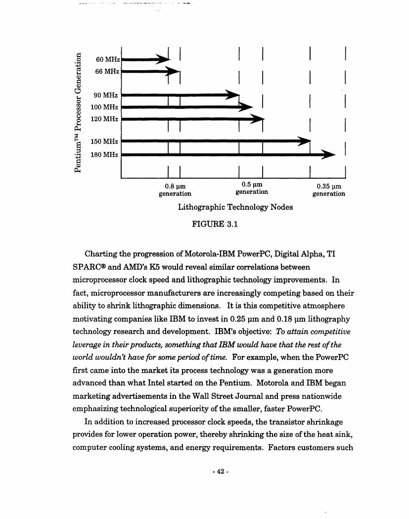
Microprocessor Clock Speed & Power Requirements Driven by Lithography
Linewidth is the primary driver of progressively faster microprocessors.
The speed of a microprocessor is determined by the speed of the six million
transistors incorporated, which is ultimately determined by each transistor's
gate width. Consider the Intel Pentium TM microprocessor as an example. The
first generation 60 MHz Pentium processor was manufactured using 0.8 pm
level lithographic technology. Process refinements on the same lithography
equipment technology allowed Intel to bring actual linewidth critical dimensions
(CD) closer to 0.7 pm.54 By tightening lithographic processes Intel was able to
introduce the 66 MHz Pentium. Speeding up the transistor is a necessary and
sufficient condition for small, 5-10%, changes in the microprocessor's frequency
response (MHz). (21007)
However, in creating the 90 MHz Pentium, merely shrinking the
transistors by using next generation 0.5 pm lithography equipment is a
necessary but not sufficient condition. Signal timing, keeping all the
components in-phase with each other, requires a complete redesign of the
Pentium processor. The benefits are a 50% speed improvement over the
original 60 MHz and 36% faster than the 66 MHz.55 Once again, Intel realized
roughly an additional 10% clock speed improvement through refining the 0.5
pm lithography process to create the 100 MHz Pentium.56 This cyclic clock
speed improvement of Pentium processors will continue for the 0.35 pm
generation products introduced in 1996, as in Figure 3.1. 57
54 0.7 pm is a rough estimate of the linewidth CD, exact dimensions are rarely releasedpublicly.
55 Disclaimer: The real-time speed of the computer the end-user realizes is not equivalentto the increased microprocessor clock speed (MHz).
56 Intel typically identifies this as 0.6 micron technology. What CD a manufacturer uses isnot necessarily equivalent to the technology generation identifiers used in the industry.
57 "Intel Offers Some Peeks in Products, Production," Electronic News, April 3, 1995, p.2 .
- 41 -
o 60 MHz
< 66 MHzCD
90 MHz0oM 100 MHz
0 120 MHz
_s
150 MHz
i, 180 MHz
, 1 I I I I 1
I I I I II I '"-I I I
11 1 1 1, 1~~~~~~~~~~~~~~~~~~~~~~~~~~11~ ~ 1[
0.8 pm 0.5 pm 0.35 ipmgeneration generation generation
Lithographic Technology Nodes
FIGURE 3.1
Charting the progression of Motorola-IBM PowerPC, Digital Alpha, TI
SPARC® and AMD's K5 would reveal similar correlations between
microprocessor clock speed and lithographic technology improvements. In
fact, microprocessor manufacturers are increasingly competing based on theirability to shrink lithographic dimensions. It is this competitive atmosphere
motivating companies like IBM to invest in 0.25 pm and 0.18 pm lithography
technology research and development. IBM's objective: To attain competitive
leverage in their products, something that IBM would have that the rest of theworld wouldn't have for some period of time. For example, when the PowerPC
first came into the market its process technology was a generation moreadvanced than what Intel started on the Pentium. Motorola and IBM began
marketing advertisements in the Wall Street Journal and press nationwideemphasizing technological superiority of the smaller, faster PowerPC.
In addition to increased processor clock speeds, the transistor shrinkageprovides for lower operation power, thereby shrinking the size of the heat sink,
computer cooling systems, and energy requirements. Factors customers such
- 42 -
as Compaq and Dell like to see in competitor microprocessor products. From a
technology standpoint during the 486 generation, Advanced Micro Devices
(AMD) originally offered smaller, cheaper, and less power-hungry
microprocessors than Intel. Essentially all the market players are using
Complementary Metal-on-Silicon (CMOS) design rules and confronting the
same technological barriers to advancement. AMD had been able to leverage
the unique capabilities of its lithography equipment supplier, ASM
Lithography, to manufacture microprocessors with tighter mask overlay
alignment tolerances. Although the linewidth CD may have been similar, with
better overlay accuracy AMD could pack transistors more closely together
providing for a smaller chip.
One prominent, high-speed microprocessor manufacturer's experience best
illustrates the importance of alignment accuracy in lithography equipment:
"With the general trend that you shrink your linewidth, you shrink theoverlay by the same amount -- we spent an extra $120,000 for astepper to make sure and get overlay from 125 nm to 105 nm. It's verycritical." (22044)
Leveraging Lower Manufacturing Costs through Lithography
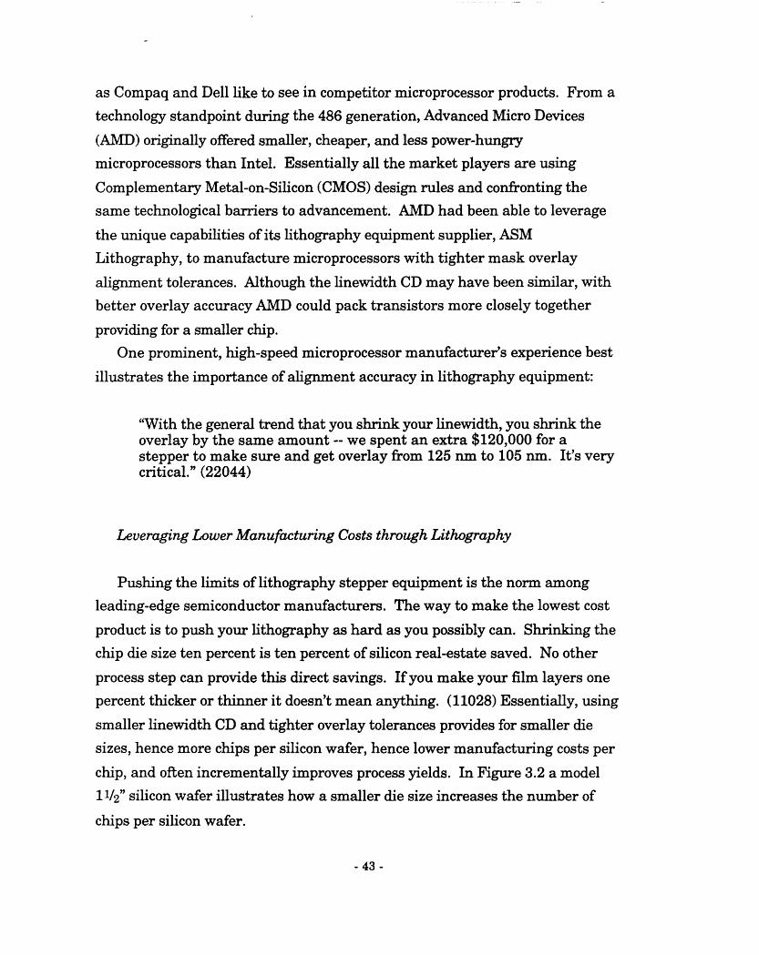
Pushing the limits of lithography stepper equipment is the norm amongleading-edge semiconductor manufacturers. The way to make the lowest cost
product is to push your lithography as hard as you possibly can. Shrinking the
chip die size ten percent is ten percent of silicon real-estate saved. No other
process step can provide this direct savings. If you make your film layers one
percent thicker or thinner it doesn't mean anything. (11028) Essentially, using
smaller linewidth CD and tighter overlay tolerances provides for smaller die
sizes, hence more chips per silicon wafer, hence lower manufacturing costs per
chip, and often incrementally improves process yields. In Figure 3.2 a model
11/2" silicon wafer illustrates how a smaller die size increases the number of
chips per silicon wafer.
- 43 -
36% smallerdie size
56 die, 5/32" Sq. 86 die, 1/8" Sq.
Illustration of die size shrinkage relationshipto number of chips per silicon wafer
FIGURE 3.2
DRAM devices have been the drivers of the most advanced lithography
technology for years because of this basic premise: the smaller the chip, the
more chips per wafer. The wafer process unit cost doesn't change based on the
number of chips on it. If IBM could produce a 10% smaller DRAM chip than
Samsung then IBM's cost is potentially 10% less than Samsung's. Overall,
costs per bit for new DRAM generations have remained competitive because of
the shrinkage associated with each lithographic technology jump. DRAMs
have seen a 4X bit-count increase per generation (4X/gen), from 1 Mb -, 4 Mb
--> 16 Mb. In each generational jump 2X/gen has come from lithographic
scaling down and 1.5X/gen from chip size increases. The remaining 1.3X/gen
has been gained from cell size reductions and architectural advances. 58
58 The National Technology Roadmap for Semiconductors (Semiconductor IndustryAssociation (SIA); San Jose, CA) December 1994, p.1 6.
- 44 -

Lithography Capital Equipment & Manufacturing Costs
Semiconductor manufacturing is a high technology business and being onthe cutting-edge is an expensive venture. During the 0.5 pm lithographicgeneration semiconductor manufacturers paid between $2.3 - $3.0 million foreach i-line stepper in their factory. An i-line stepper for the 0.35 pm generation
technology is comparably around $3 million. Those semiconductor
manufacturers which venture into the newer deep-ultraviolet (DUV)lithography equipment expect to pay roughly $3.6 - $4.2 million per machine.(51132) This typifies the escalation of capital equipment costs prevalent in the
semiconductor industry at this time.Overall, a flourishing semiconductor company's capital equipment
expenditures average 25% of annual revenues, unprecedented by any otherindustry.59 Comparing the capital expenditures with the revenues ofsemiconductor manufacturers clearly illustrates the extent of the industry'sinvestments, Table 3.1 and 3.2. Lithography equipment represents nearly a
third of any given semiconductor company's capital purchases.SIA's 35% figure is frequently cited as the proportion of the industry's
capital costs dedicated to lithography technology.6 0 Functionally, lithographyin the semiconductor manufacturing world includes metrology, scanning
electron microscopy (SEM), tracking systems, as well as stepper equipment.A 0.5 pm generation, 5000 wafer starts-per-week (WSPW) volume fab has
grown to become a $1 billion investment. Capital equipment is about $500million, with the lithography function costing -$165 million with 30 sub-
systems. Henceforth, roughly 33% of capital equipment costs are for thelithography function. Independently, lithography stepper equipment isestimated to be more on the order of 15-20% of capital equipment costs for a
new fab. (12040)
59 Intel Tops VLSI Research Rankings; Korean Vendors Growing Fast" Electronic News,November 14, 1994, p.80.
60 The National Technology Roadmap for Semiconductors, (SIA; San Jose, CA) December1994, p.8 1.
- 45 -
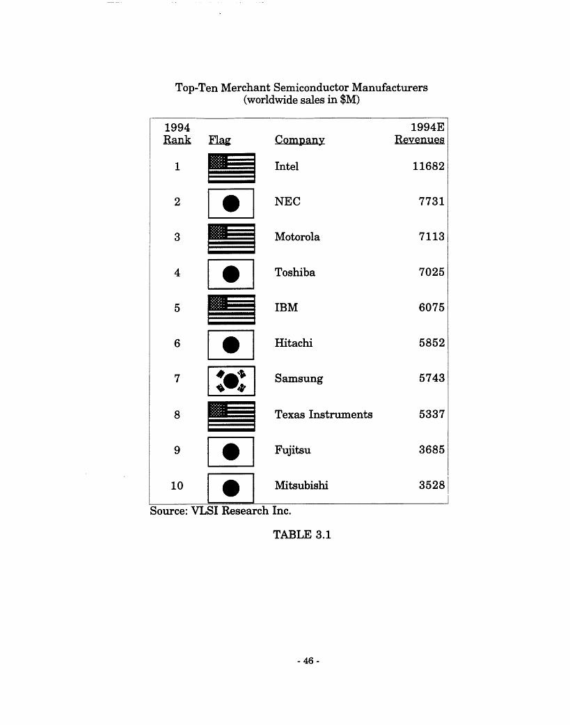
Top-Ten Merchant Semiconductor Manufacturers(worldwide sales in $M)
1994Rank Flag
1
2 O
1994ERevenues
11682Intel
NEC
Motorola
Toshiba
3
7731
7113
70254 ·
5
6 W
7 _ _ _9 I
10
IBM
Hitachi
Samsung
Texas Instruments
Fujitsu
Mitsubishi
Source: VLSI Research Inc.
TABLE 3.1
- 46 -
6075
5852
5743
5337
3685
3528
_112M--
- -0
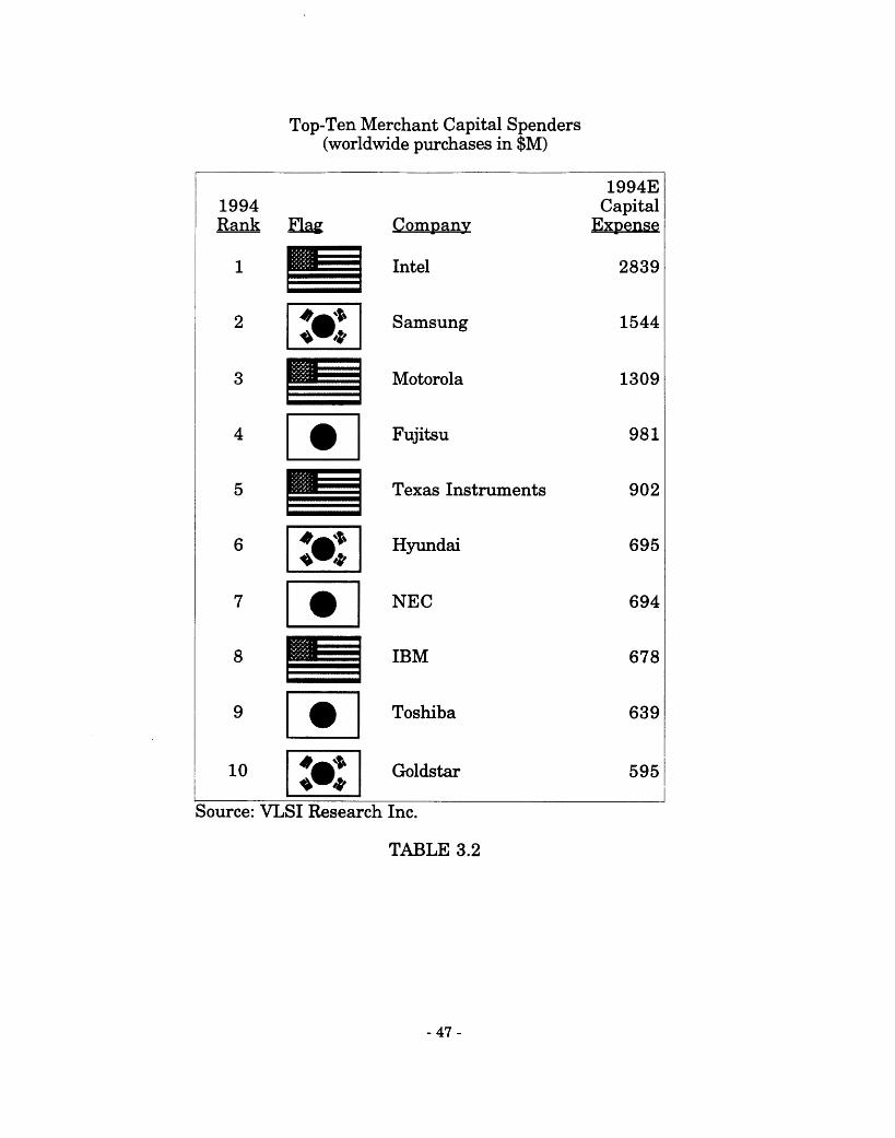
Top-Ten Merchant Capital Spenders(worldwide purchases in $M)
Flag Company
1 i
2 _ 1_
l l
3
4 $0i
5
6 II
8
9
10 I °v" 1l s_=_l19o0
Intel
Samsung
Motorola
Fujitsu
Texas Instruments
Hyundai
NEC
IBM
Toshiba
Goldstar
Source: VLSI Research Inc.
TABLE 3.2
- 47 -
1994Rank
1994ECapital
Expense
2839
1544
1309
981
902
695
694
678
639
595
�I

Of course, not everyone is building $1 billion scale fabs. Nonetheless, in
terms of cost criticality, manufacturers concur that photolithography is the
single largest manufacturing investment, above and beyond chemical vapordeposition (CVD), etch, or thermal processes. (11011) Fab lines are almost
always centered around lithography equipment. Manufacturing throughput is
largely determined by lithography throughput, often intentionally.
Extent of Lithography Equipment Criticality to Semiconductor Products
Given the consumer market drivers for faster, cheaper semiconductor
devices and the magnitude of capital investments associated, leading-edgemanufacturers are pushing the limits of new lithographic equipment
capabilities. Particularly in linewidth CD and alignment accuracy,manufacturers of memory and microprocessor devices are operating at 90-
100% of the limits of their lithography machine's specified capabilities. A
select number of manufacturers track process capability index, Cpk,
performance metrics for linewidth CD. (12042)
However, not all semiconductor products, and only a 25% of a given leading-
edge product, utilizes the most advanced lithographic capabilities available.
Rising equipment costs, and common sense, has semiconductor
manufacturer's mixing lithographic equipment from previous generations with
the most advanced equipment. For example, among the microprocessor
manufacturing companies surveyed, currently about 25% of the lithographyequipment on the manufacturing floor is going to be leading-edge, 0.35 Pm
capable. This implies that roughly 25% of the mask layers for a Pentium,
PowerPC, Alpha, or SPARC chip is critical level. (11036)
- 48 -

Worldwide Lithography Stepper1993 Market Shares
OthersUltratech 8%
ASI69
52%Nikon
2%. IIL %-v JL&
FIGURE 3.3
Limited Supply Base for Leading-edge Lithography Tools
Worldwide there are only four leading-edge suppliers of leading-edge
lithography equipment technology: Nikon, Canon, ASM Lithography, and
Silicon Valley Group Lithography (SVGL). By leading-edge it is implied thatthese suppliers are capable of supplying lithography solutions for 0.5 m, 0.35
pum, and 0.25 pm generations in a timely manner. Figure 3.3 outlines the 1993worldwide market shares of all optical lithography equipment manufacturers. 61
Nikon has been the market share leader of the industry since the late 1980s.SVGL has been in existence for many years but has only recently become in acompetitive position offering lithography equipment to the open market.
61 "VLSI Report -- Special Survey XVII: '93-'94 Semiconductor Manufacturing Equipmentand Materials Industry," U.S. Joint Publications Research Service, JPRS-JST-94-035-L,Foreign Broadcast Information Service, 14 July 1994.
- 49 -

Ultratech Stepper, Inc. specializes in > 0.8 pm high-throughput lithography
equipment. Ultratech pioneered the concept of mix-and-matching leading-edge
lithography equipment with high-throughput equipment for noncritical layers.
Since then nearly every lithography equipment supply has followed suit in
providing manufacturers a selection of critical-level and non-critical level
steppers. Leading-edge suppliers are limited in number by the unique technical
capabilities required, driving a high cost barrier for market entry bycompetitors, as outlined further in section 3.2.
Lithography Criticality in Summary
Lithography is the driving technology for the semiconductor industry. No
other manufacturing function provides the leverage to feed customer demands
for faster, smaller, cheaper products. No other process step requires nearly as
significant a portion of capital equipment and manufacturing costs. CVD,
etch, and thermal processes are undoubtedly all essential for fabricating a
functional integrated circuit. However, it is having the most advanced
lithographic equipment which determines if you are a leading-edge
semiconductor manufacturer or not.
3.2. The Make-Buy Spectrum: Industry Focus on Supply ChainManagement
Ironically, despite the fact that lithography plays such a central role in
semiconductor manufacturing, internal development of lithography equipmenttechnology is practically unheard of today among U.S. semiconductor
companies. The locus of lithography knowledge and sources of innovation rests
in the external matrix of equipment supplier companies. As a result, the
industry relies upon the supplier base for lithographic capabilities.
Semiconductor companies have gradually divested from equipment
manufacturing over the last two decades. Surprisingly, lithography equipmentwas one of the earliest technologies to be out-sourced by manufacturers. The
- 50 -
_ - ___ __ -" __ � -, - " __ _.' - - - - -1 11
last company in the world vertically integrated to be a lithography equipmentdeveloper and a major semiconductor producer was Hitachi. Since the late
1980s, Hitachi has been unable to keep pace with the technological
improvements of market leaders Nikon and Canon. In 1993 Hitachi
announced that it was freezing development of next-generation equipment and
withdrawing from the business. Hitachi's equipment was intended mostly for
its own use, and the company has struggled with outside sales. The cost of
development has increased with each successive generation and it appears
this has driven Hitachi's decision to withdraw from the optical stepper
equipment manufacturing. However, Hitachi continues to have significant
manufacturing capabilities in electron-beam lithography equipment, plasmaand metal etching equipment, and scanning electron microscopes (SEM), just
to name a few.62
Most U.S. semiconductor companies never even attempted to develop
internal capabilities because they never had an impetus to build up anexpertise in optical stepper equipment. Lithography suppliers had been
always been able to supply industry needs. In the U.S. only AT&T Bell Labs
and IBM have retained a degree of lithography technology development
knowledge, but have long ago given up the concept of building their own optical
lithography equipment. (31021) During the 1970s and prior, semiconductor
manufacturers internally made optical exposure equipment called 'aligners' ata time when the industry was young and the supporting technology
infrastructure largely undeveloped. By the time the industry transitioned tooptical stepper equipment technology no U.S. semiconductor companies had
the desire to internally make optical lithography equipment.
The two key issues creating a reliance on suppliers: (1) The unique
technical expertise necessary for the design and manufacture of lithographyequipment resulting in (2) The costs of maintaining lithography equipment
technology knowledge and manufacturing capability in-house became
prohibitively high for any one semiconductor company to afford. The degree of
62 "VLSI Report --" JPRS-JST-94-035-L, 14 July 1994, prev. cited.
- 51 -
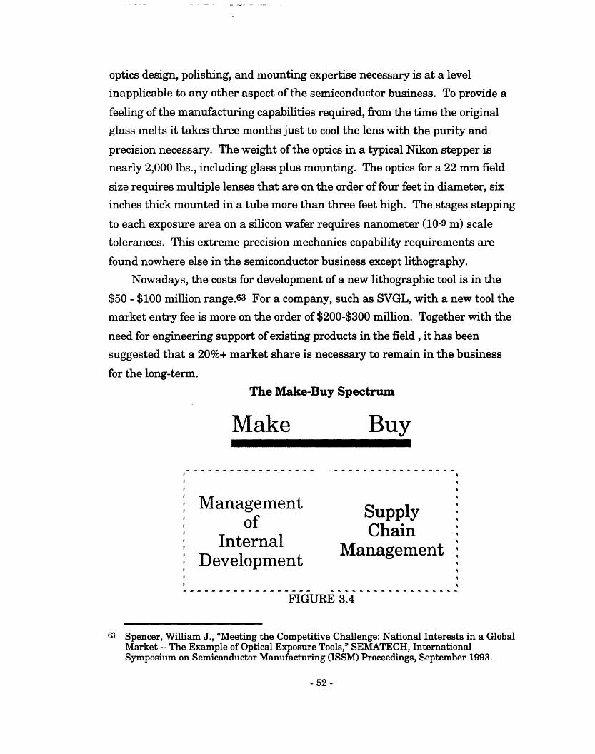
optics design, polishing, and mounting expertise necessary is at a level
inapplicable to any other aspect of the semiconductor business. To provide a
feeling of the manufacturing capabilities required, from the time the original
glass melts it takes three months just to cool the lens with the purity and
precision necessary. The weight of the optics in a typical Nikon stepper is
nearly 2,000 lbs., including glass plus mounting. The optics for a 22 mm field
size requires multiple lenses that are on the order of four feet in diameter, six
inches thick mounted in a tube more than three feet high. The stages stepping
to each exposure area on a silicon wafer requires nanometer (10-9 m) scale
tolerances. This extreme precision mechanics capability requirements are
found nowhere else in the semiconductor business except lithography.
Nowadays, the costs for development of a new lithographic tool is in the
$50 - $100 million range.63 For a company, such as SVGL, with a new tool the
market entry fee is more on the order of $200-$300 million. Together with the
need for engineering support of existing products in the field , it has been
suggested that a 20%+ market share is necessary to remain in the business
for the long-term.
The Make-Buy Spectrum
Make Buy
Management Supplyof upplyof ChainInternal Management
Development
FIGURE 3.4
63 Spencer, William J., "Meeting the Competitive Challenge: National Interests in a GlobalMarket -- The Example of Optical Exposure Tools," SEMATECH, InternationalSymposium on Semiconductor Manufacturing (ISSM) Proceedings, September 1993.
- 52 -
Years ago, when incorporating lithography technology into their
manufacturing process, semiconductor companies essentially had a choice to
make along the "Make-Buy" Spectrum, Figure 3.4. The choice was either to
"Make" and manage the internal development of lithography technology or
"Buy" the equipment thereby requiring technology supply chain management.The fact is semiconductor manufacturers have chosen to buy and have been
buying lithography equipment from suppliers since the late 1970s.Semiconductor manufacturers realized their core competencies are in
manufacturing process integration and chip design. The internal capabilities
along the Make-Buy spectrum are on the order of being able to create
specifications, evaluate equipment options, and make software adjustmentsnecessary for operation as part of the manufacturing process. Nearly all U.S.
semiconductor manufacturers contract the maintenance of lithographyequipment with their suppliers. As far as equipment maintenance is
concerned, it is believed the opposite is true among Japanese semiconductor
producers. With the exception of IBM, internal lithographic capabilities are
kept at a minimum level to maintain the knowledge for equipment evaluation,full operational abilities, and possibly a selection of lithography process
support technologies, i.e. resists and masks.
3.3. Cyclicality: The Industry-wide Equipment Sourcing Cycle
Supply-Side Lithography Equipment Market Cyclicality
One of the challenges confronted by the semiconductor equipment suppliers
is surviving the peaks and troughs of manufacturer's buying patterns. This
cycle is largely driven by the technology advances of lithography equipment.
Since the mid 1980s the historic pattern has been to advance technological
capabilities for DRAM bit count by a factor of four (4X) every four years. This
has pressured suppliers to provide the appropriate lithography equipment tomeet the needs of DRAM manufacturers on the leading-edge.
- 53 -
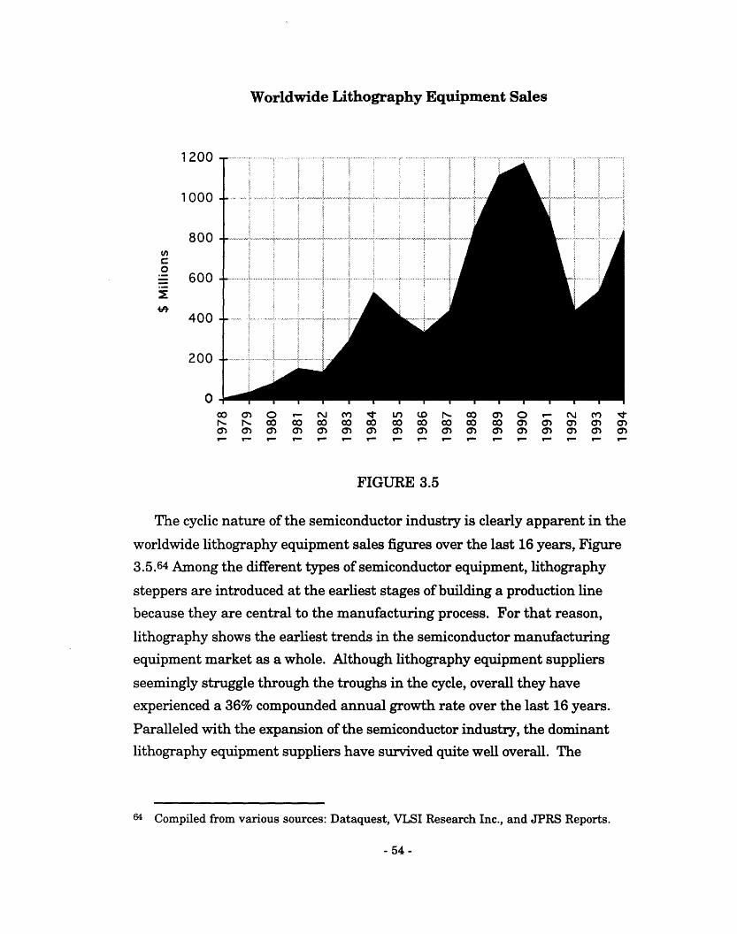
Worldwide Lithography Equipment Sales
1 )nI LVV
1000.
800.c
600
400.
200.
0.00 O O N cX) 1- uf ( ) en O 0 N r -n N O CO CO C CO CO O CO CO CO a) ) O O a
FIGURE 3.5
The cyclic nature of the semiconductor industry is clearly apparent in the
worldwide lithography equipment sales figures over the last 16 years, Figure3.5.64 Among the different types of semiconductor equipment, lithography
steppers are introduced at the earliest stages of building a production line
because they are central to the manufacturing process. For that reason,
lithography shows the earliest trends in the semiconductor manufacturingequipment market as a whole. Although lithography equipment suppliers
seemingly struggle through the troughs in the cycle, overall they haveexperienced a 36% compounded annual growth rate over the last 16 years.
Paralleled with the expansion of the semiconductor industry, the dominantlithography equipment suppliers have survived quite well overall. The
64 Compiled from various sources: Dataquest, VLSI Research Inc., and JPRS Reports.
- 54 -
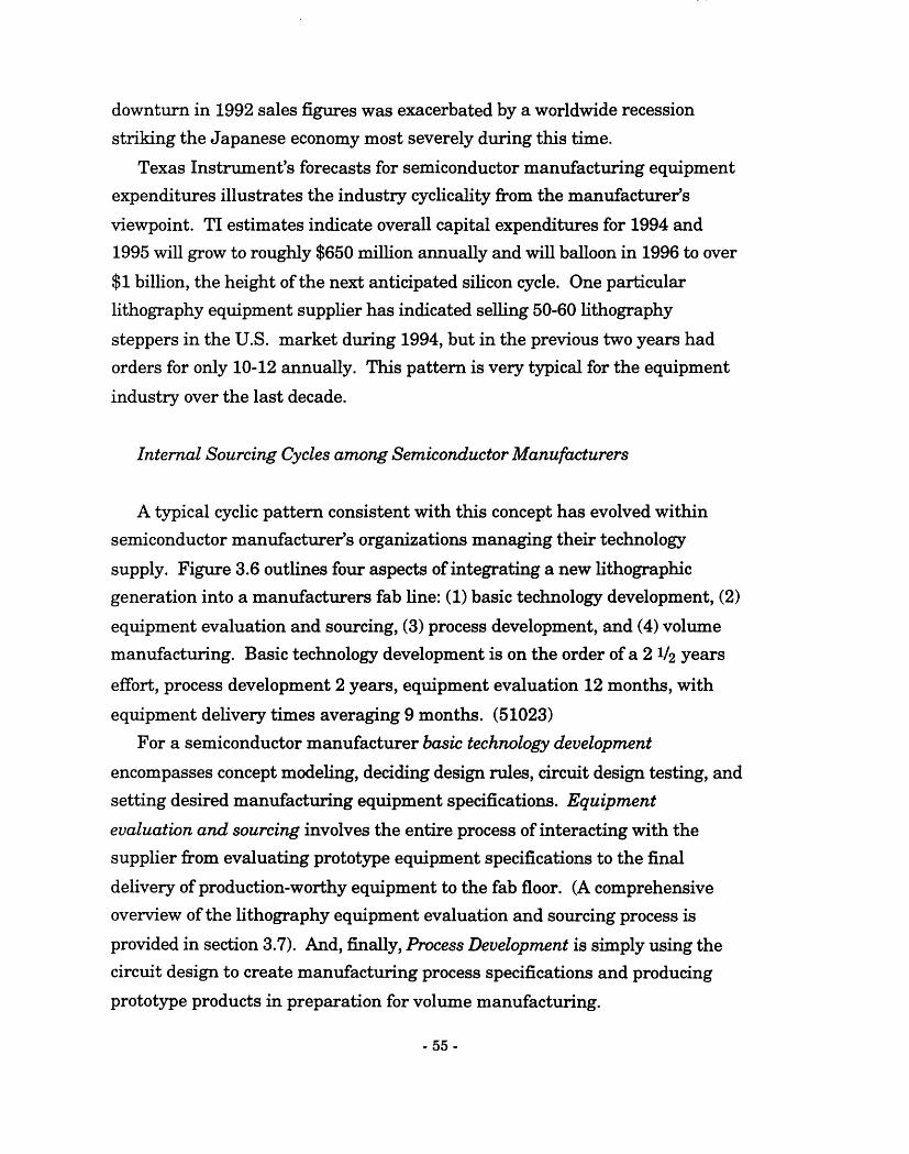
downturn in 1992 sales figures was exacerbated by a worldwide recession
striking the Japanese economy most severely during this time.
Texas Instrument's forecasts for semiconductor manufacturing equipment
expenditures illustrates the industry cyclicality from the manufacturer's
viewpoint. TI estimates indicate overall capital expenditures for 1994 and
1995 will grow to roughly $650 million annually and will balloon in 1996 to over
$1 billion, the height of the next anticipated silicon cycle. One particular
lithography equipment supplier has indicated selling 50-60 lithography
steppers in the U.S. market during 1994, but in the previous two years hadorders for only 10-12 annually. This pattern is very typical for the equipment
industry over the last decade.
Internal Sourcing Cycles among Semiconductor Manufacturers
A typical cyclic pattern consistent with this concept has evolved withinsemiconductor manufacturer's organizations managing their technology
supply. Figure 3.6 outlines four aspects of integrating a new lithographic
generation into a manufacturers fab line: (1) basic technology development, (2)
equipment evaluation and sourcing, (3) process development, and (4) volume
manufacturing. Basic technology development is on the order of a 2 1/2 years
effort, process development 2 years, equipment evaluation 12 months, with
equipment delivery times averaging 9 months. (51023)For a semiconductor manufacturer basic technology development
encompasses concept modeling, deciding design rules, circuit design testing, and
setting desired manufacturing equipment specifications. Equipment
evaluation and sourcing involves the entire process of interacting with thesupplier from evaluating prototype equipment specifications to the final
delivery of production-worthy equipment to the fab floor. (A comprehensive
overview of the lithography equipment evaluation and sourcing process is
provided in section 3.7). And, finally, Process Development is simply using the
circuit design to create manufacturing process specifications and producing
prototype products in preparation for volume manufacturing.
- 55 -
Stages of Internal Technology Development forVolume Manufacturing
Basic Technology Development Process Development Manufacturing
ent Evaluation & Sourcing i -, r ' 1 -A
-9 months month +12 months
Evaluate Prototype OrderPrototype In-house, ProductionEquipment Development EquipmentOptions Begins forFabs
-12months +9 months
Determine Peak ofDesired EquipmentEquipment EvaluationSpecifications Process
f-
+24 mon
First SiliconVolumeProductionBegins
+21 months
BeginReceivingProductionEquipment
FIGURE 3.6
For a given lithographic generation this process is on average a 4 year
venture. For example, take Intel's introduction of 0.35 pm generationtechnology into their PentiumTM microprocessor product line. Let's assume
Intel began volume production of Pentium microprocessors using 0.35 pm
generation equipment in January 1995. Roughly around January 1993, 24
months earlier, Intel began process development for the 100 MHz Pentium
design. And probably as far back as January 1992 Intel began to determine
the critical dimension (CD) and overlay accuracy metrics needed in the
specifications for 0.35 pm generation equipment. This is the typical cycle
every semiconductor manufacturer in the industry follows. Of course, theexact time duration and starting time varies within each company.
Although everyone within the semiconductor industry understands thebasic framework for internal technology development, many companies had
difficult identifying further detailed steps. The 3-4 year time constant for
technology and process development seems to make standardizing the steps
difficult as organizations evolve. (31014) More importantly, the
semiconductor industry is noteworthy for a high degree of employee migration
- 56 -
-24 months
BeginExplorationof NextGeneration
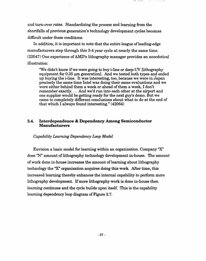
and turn-over rates. Standardizing the process and learning from theshortfalls of previous generation's technology development cycles becomes
difficult under these conditions.
In addition, it is important to note that the entire league of leading-edge
manufacturers step through this 3-4 year cycle at nearly the same time.(22047) One experience of AMD's lithography manager provides an anecdotical
illustration:
"We didn't know if we were going to buy i-line or deep-UV [lithographyequipment for 0.35 pm generation]. And we tested both types and endedup buying the i-line. It was interesting, too, because we were in Japanprecisely the same time Intel was doing their same evaluations and wewere either behind them a week or ahead of them a week, I don'tremember exactly... And we'd run into each other at the airport andone supplier would be getting ready for the next guy's demo. But wecame to completely different conclusions about what to do at the end ofthat which I always found interesting." (42064)
3.4. Interdependence & Dependency Among SemiconductorManufacturers
Capability Learning Dependency Loop Model
Envision a basic model for learning within an organization. Company "X"
does "N" amount of lithography technology development in-house. The amount
of work done in-house increases the amount of learning about lithography
technology the "X" organization acquires doing this work. After time, this
increased learning thereby enhances the internal capability to perform more
lithography development. If more lithography work is done in-house then
learning continues and the cycle builds upon itself. This is the capability
learning dependency loop diagram of Figure 3.7.
- 57 -
Capability Learning Dependency Loop
Amount of WorkDone In-house
N\
Internal AmCapability Let
ount ofarning
FIGURE 3.7
However, the loop can work to positively re-inforce internal capability or
negatively. This is the state-of-affairs in the U.S. semiconductor industry. The
limited amount of lithography development done in-house has steadily reduced
learning of the most advanced lithography technologies, hence internalcapability has fallen in parallel. Dependency on the lithography equipment
supplier has come to the level were manufacturers are purchasing off-the-shelfequipment ready for volume manufacturing of their products without
modifications. (51023) Likewise, equipment maintenance is largely contracted
out from supplier. The costs associated with maintaining an internal
knowledge based is assumed to be far greater than having contracted services.(51025)
- 58 -
The Metrics and Investment in Internal Lithographic Capabilities
Measuring a semiconductor companies internal capabilities can be
characterized by their activities in three areas: (1) lithography equipment
development activities, in terms of optical steppers or advanced equipment
technologies, (2) internal mask fabrication and development activities, and (3)
internal resist fabrication and development activities. Masks and resists arethe core supporting lithographic technologies essential for the practical
operation of a lithograph tool. SVGL could create the world's greatest 0.25 Pum
deep-ultraviolet step-and-scan lithography equipment, but without equally
capable and production worthy resist and mask technologies the tool would be
useless to semiconductor manufacturers.
Each leading-edge American semiconductor manufacturer has, on average,
35 personnel focused on lithography basic technology research, process
engineering, and equipment engineering. It appears that having a minimum of
25-30 people is the critical mass necessary for performing lithography
technology development and sourcing within a leading-edge company. This
implies that in order to effectively convert raw manufacturing technology into
a viable lithography process, companies typical investment in human capitalknowledge is on the order of $1.5 million annually (based on $42,000 average
gross annual salary). (11116) These numbers don't include the number of
lithography engineers, maintenance, or operators of each individual fab, but
merely the countable centralized personnel focused on lithography technology
within each given manufacturer.
Internal Optical Stepper Equipment Technical Capabilities
The degree of internal lithography equipment capabilities among U.S.
semiconductor manufacturers has been alluded to frequently in the prior
sections of this text. With the possible exception of IBM, the typical limits of a
semiconductor company's equipment capabilities is making specifications,
testing the equipment functionality, and using the equipment to its fullest.
- 59 -
Everything short of being able to make modifications to the equipment's
components.
Process development and manufacturing system integration is really thecore competence of semiconductor companies. One manufacturer's viewpoint
illustrates the general state-of-affairs among the leading-edge companies:
"We treat the equipment in development just like it was productionequipment ... We want to use it, we don't want to play with it, we wantto use it. We do certain things with steppers for example, we definitelyexplore modified illumination schemes and phase-shift masks ... But,our primary interest is using it to help develop silicon products. Not todevelop steppers. Now, we talk with the stepper suppliers, particularlyNikon and Canon, and we certainly feedback what changes we would liketo see ... But, we don't actually do any mechanical engineering,software, or any development per se, no optics, etc. And, that'sbasically always been the case." (31021)
Internal Mask Houses & Technology Development
The typical independent U.S. mask suppliers in the industry include
Photronics, Toppan and DuPont. There is seemingly a bi-modal distribution of
internal mask capabilities among leading-edge semiconductor companies.
Fundamentally, (1) either companies have minimum internal capability andout-source the mask manufacturing completely, or (2) companies have
internal mask manufacturing capabilities, as well as out-source to manage
capacity or out-source higher/lower technically challenging mask
manufacturing jobs. An example of the companies with each strategy is
outlined in Table 3.3.
- 60 -
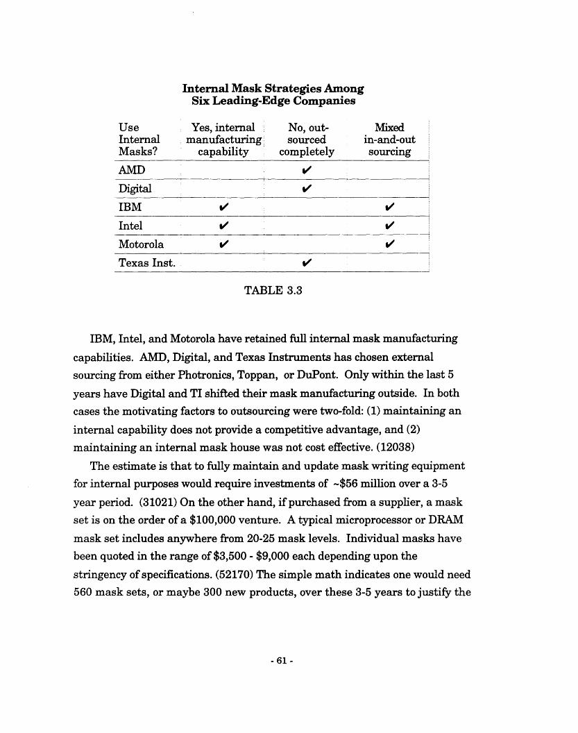
Internal Mask Strategies AmongSix Leading-Edge Companies
Use Yes, internal No, out- MixedInternal manufacturing sourced in-and-outMasks? capability completely sourcing
AMD
Digital V
IBM v vIntel v v
Motorola V V
Texas Inst. V
TABLE 3.3
IBM, Intel, and Motorola have retained full internal mask manufacturing
capabilities. AMD, Digital, and Texas Instruments has chosen external
sourcing from either Photronics, Toppan, or DuPont. Only within the last 5
years have Digital and TI shifted their mask manufacturing outside. In bothcases the motivating factors to outsourcing were two-fold: (1) maintaining an
internal capability does not provide a competitive advantage, and (2)
maintaining an internal mask house was not cost effective. (12038)
The estimate is that to fully maintain and update mask writing equipmentfor internal purposes would require investments of -$56 million over a 3-5
year period. (31021) On the other hand, if purchased from a supplier, a maskset is on the order of a $100,000 venture. A typical microprocessor or DRAM
mask set includes anywhere from 20-25 mask levels. Individual masks havebeen quoted in the range of $3,500 - $9,000 each depending upon the
stringency of specifications. (52170) The simple math indicates one would need
560 mask sets, or maybe 300 new products, over these 3-5 years to justify the
- 61 -
return-on-investment. 65 For the wide diversification of products within
Motorola and IBM it is reasonable to believe they can cost effectively maintain
an internal capability by cost measures.66 Intel, alternatively, may bemaintaining an internal mask facility as an investment in intellectual property
protection of their microprocessor circuit designs imprinted on lithography
masks.
Mask making is clearly viewed among the industry as a pre-competitive
technology. The intercommunication among Motorola, IBM, and Intel's masks
houses are seemingly frequent. As well, it has not been uncommon for Digital,
for example, to assist DuPont on mask manufacturing reliability issues.
(31021)
Internal Resist Technology Development
Leading-edge resist suppliers include Shipley, JSR, Sumitomo, TOK, OCG,
AZ, AT&T and IBM. IBM is the only U.S. merchant semiconductor
manufacture with an internal resist facility. IBM's Resist Facility hasconsistently been on the leading-edge and is the only viable deep-ultraviolet
resist available on the market, as of early 1995. However, IBM's resist facility
hasn't historically been a competitive supplier on the open market. (31021)
As with optical stepper equipment, the industry relies upon suppliers andinvests internally in maintaining an expertise in characterizing the
performance of the various resists on the market. Each semiconductorcompany may have a half dozen or fewer resist specialists assisting their
process development and characterization efforts.
66 Often there will be multiple exact copies of a mask set for a single product. Generallythis is to have duplicate copies at a single fab site for more flexible process flows or whenmanufacturing the same product at multiple fab sites. These calculations are bestestimates based on available numbers.
66 It is understood that Motorola treats its Mask House as a profit center. IBM hasn'tclearly indicated whether its Burlington Mask Facility is subject to cost scrutiny or not.
- 62 -

Dependency Molds Semiconductor Equipment Technology Management Style
The lack in in-house lithography capability has forced interdependency
among U.S. semiconductor manufacturers. Learning is achieved via industry-
wide consortia such as Sematech, Semiconductor Industry Association (SIA),
and the Semiconductor Research Center (SRC). Long-term research anddevelopment of lithography technology has been exported to the academic and
supplier community. Semiconductor manufacturers provide financial support
of long-term research activities coordinated by the SRC. The SRC's primary
function is to decide upon appropriate 5-10 years advanced research projects
at U.S. colleges and universities. Individually, some manufacturers support
various academic research projects on a case-by-case basis, but this is rare.One case example would be between TI and the Interuniversity
Microelectronics Center (IMEC), University at Louven, Belgium, researching
optical lithography options for 0.18 pm technology 1-Gigabit DRAMs.67
(61022)
Dependency on lithography equipment suppliers also means the
opportunity to gain competitive advantage through technology has diminished.Open-access to leading-edge lithography technology makes the capability
available to all who can afford the capital investment. What has become
critically important, however, is the ability to keep up-to-date with your
competitors who are purchasing the most advanced technology. To some
degree, manufacturers compete on their ability to leverage suppliers to provide
them with the newest generation equipment in a timely manner. Having apreferential relationship with the supplier could give a company better access
to the newest technical capabilities. This was the case for AMD when it was
initially able to attain better alignment accuracy specifications from its
supplier that Intel. This originally provided AMD with the ability to produce
smaller 486-class MPUs than Intel. Since this time Intel has been able to
67 "TI, IMEC Join in Lithography R&D" Electronic News, Feb. 27, 1995, p.56.
- 63 -

leverage its supplier such that the differences in 486-class chip dimensions is
no longer an issue.
Leading-edge semiconductor manufacturers generally receive their first
production worthy next-generation lithography equipment usually within 6-9
months of each other. For example, 0.5 pm equipment was acquired by all of
these manufacturers by 2Q1992 *6 months. (11110) Likewise, for 0.35 pm
lithography, manufacturers began receiving prototype equipment as early as
1Q1994 with the latest reported start of 0.35 pm level technology by 2Q1995.
(11026)
According to manufacturer's, the 6-9 month variation in availability of
next-generation technology provides minimal competitive advantage. Marketconditions for microprocessors in the semiconductor industry provide little
advantage to having a six month technology lead. In DRAMs, in contrast,being first to market with the next-generation 64 Mb chips means you can set
the market price high, given the limited supply. Market dominance for the
'first to market' manufacturer is limited to those first 6-9 months. Typically,
one can purchase four 16 Mb sets at extremely competitive prices compared
to one 64 Mb set. The true return-on-investment analysis of these market
leaders requires further study.Nonetheless, the bottom line concept: suppliers determine the progression of
lithography technology advancement. Motivating continuous improvement in
the free-market atmosphere implies ensuring multiple suppliers attain
competitive capability and drive to move the technology forward. To achieve
this end manufacturers have chosen, unknowingly, a simple philosophy:
"Minimize capital expenditures while maximizing supplier switching flexibility."Maximizing supplier switching flexibility has evolved to mean: (1) have the
ability to easily switch to the most technically competent supplier, or (2)
maintain the threat of being able to switch suppliers if your strategic partner
fails. Minimizing capital expenditures is may be an obvious concept, but in this
context it further implies: (1) seek the opportunity for volume purchasing from
a single supplier to attain the economies-of-scale in equipment pricing, and (2)avoid the hidden costs of switching suppliers.
- 64 -
The expertise of semiconductor companies has become to characterize the
performance of equipment and supporting lithography technologies as it suites
their manufacturing process needs. As a strategy to ensure some
independence for the supplier, a subset of manufacturers avoid designing their
process around any one specific equipment set. (12043) Ideally, the
semiconductor manufacturing process would be totally independent of the
lithography equipment supplier, purchased off-the-shelf, with the samespecifications. In reality, this doesn't occur. The details of mask design is
dependent upon which lithographic tool is being used for circuit patterning. For
example, a mask designed for a Canon stepper would not function correctly on
a Nikon, and vice versa.
Assessing Supplier Switching Costs
Semiconductor manufacturers have a difficulty giving a numeric costassociated with switching suppliers. However, four core concepts surfaced
repeatedly: (1) the learning curve of process engineers to optimize performance
on unfamiliar equipment, (2) mask alignment systems between
manufacturer's tools are totally different and requires experiential knowledgeto correctly model, (3) the support infrastructure, in terms of maintenance
personnel and parts, changes with the name-brand of the equipment, and (4)relationships with established suppliers is easier to maintain than to go
through the mutual learning curves of creating a new relationship with analternative supplier. (11028)
The potential switching costs incurred by a given company is largelydetermined by their internal corporate equipment sourcing strategy. A
semiconductor manufacture with a more centralized approach to lithographysourcing will incur greater switching costs than a diversified, decentralized
manufacturer. Before evaluating relative switching costs it first becomesnecessary to understand how companies have organized their semiconductor
lithography equipment sourcing approach.
- 65 -

3.5 Internal Corporate Equipment Sourcing Strategies
Semiconductor manufacturers have a spectrum of organizationalinfrastructures to cope with the cyclic process of incorporating new
lithographic technologies. The fundamental organization of a semiconductor
company at the manufacturing level is composed of three spheres of influence:
process\ equipment development, manufacturing equipment technologyorganizations, and the fabrication lines. In some companies these three
spheres are clearly delineated, others combine these functions together intoone group. Typically there is always a clear distinction between those
responsible for sourcing of equipment and those personnel working on process
development. The fab is inevitably the site of integration, as in Figure 3.6.
Three Spheres in theSemiconductor Realm
Pr cing
ProcessEquipment
Development
Infc. Ean.Technology
Organization
FIGURE 3.8
- 66 -
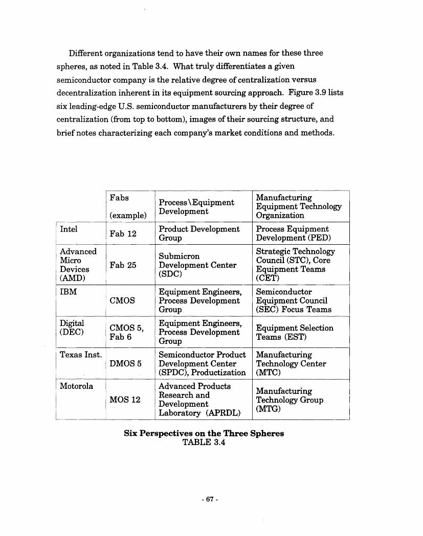
Different organizations tend to have their own names for these three
spheres, as noted in Table 3.4. What truly differentiates a given
semiconductor company is the relative degree of centralization versus
decentralization inherent in its equipment sourcing approach. Figure 3.9 lists
six leading-edge U.S. semiconductor manufacturers by their degree of
centralization (from top to bottom), images of their sourcing structure, and
brief notes characterizing each company's market conditions and methods.
Intel
AdvancedMicroDevices(AMD)
IBM
Digital(DEC)
Texas Inst.
Motorola
Fabs
(example)
Fab 12
Fab 25
CMOS
CMOS 5,Fab 6
DMOS 5
MOS 12
Process \ EquipmentDevelopment
Product DevelopmentGroup
SubmicronDevelopment Center(SDC)
Equipment Engineers,Process DevelopmentGroup
Equipment Engineers,Process DevelopmentGroup
Semiconductor ProductDevelopment Center(SPDC), Productization
Advanced ProductsResearch andDevelopmentLaboratory (APRDL)
ManufacturingEquipment TechnologyOrganization
Process EquipmentDevelopment (PED)
Strategic TechnologyCouncil (STC), CoreEquipment Teams(CET)
SemiconductorEquipment Council(SEC) Focus Teams
Equipment SelectionTeams (EST)
ManufacturingTechnology Center(MTC)
ManufacturingTechnology Group(MTG)
Six Perspectives on the Three SpheresTABLE 3.4
- 67 -
.. -

Centralization - Decentralized Equipment Sourcing Practices
IntelFab 4 _ Fab I* Total centralization
Fa Fab . * Limited product line· "Copy Exactly" processes· Internal dedicated mask fabrication
Fab Fab Fab * Industry role model strategy
Advanced Micro DevicesFab Fab * Centralized with limited variance
· Limited product line· Product fabs with similar process
FujD- u*· Resist, Masks single supplier sourceFab Fab Fujitsu * Deviation in Joint Venture Fab
FabIBM Microelectronics
8 I emquiment y * Newly centralized equipment selection>0.8 gm masks 0.5 Fabm Single-sourced internal mask house
FaFcassab · Resist recommendations to fabs* Processes independently developed
Digital Equipment Corp..5 m l- masks l •0.35 *m : Independent equipment selection
Fabs m "-' Fabs · Few fabs with dedicated product lines....as..X · Single sourced mask supplier tied
· Geographic proximity with Shipley
Texas Instruments.. men. * Newly implemented central sourcing
0.8 Fabs pm ar SiL • 0.5 m * Restricted choice equipment selectionFabs -. r~.A-t Fabsy F b *o Independent masks, resists, processes* Key product processes centralized
equipment, masks, resist Motorola SPSp-ro4esses A-X 32+ · Highly decentralized, independent fabs
- - - - -- - -- Q _o_* ~ non n innv nn icprocess Y World- * Key products with centralized processprOcZ Wide * Matrix organization between fabs
FIGURE 3.9
- 68 -
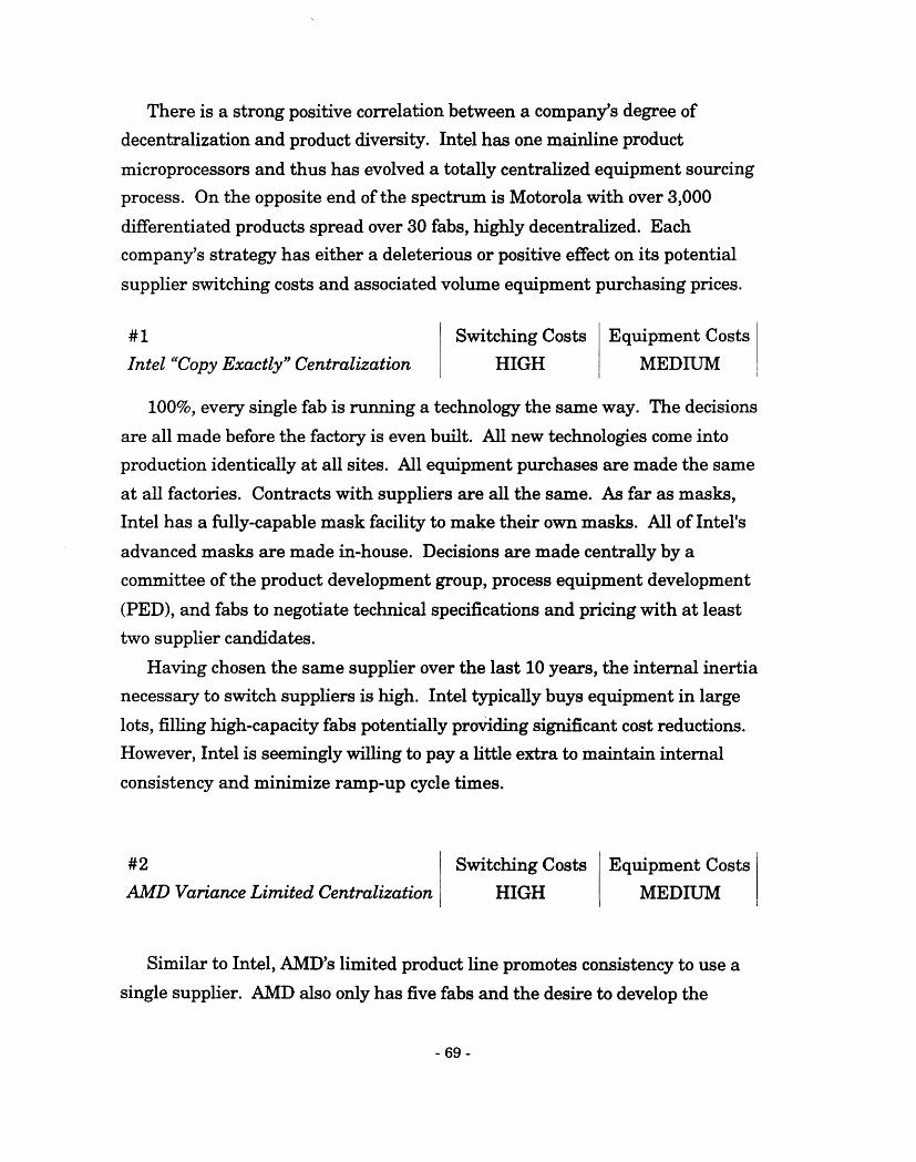
There is a strong positive correlation between a company's degree of
decentralization and product diversity. Intel has one mainline product
microprocessors and thus has evolved a totally centralized equipment sourcingprocess. On the opposite end of the spectrum is Motorola with over 3,000
differentiated products spread over 30 fabs, highly decentralized. Each
company's strategy has either a deleterious or positive effect on its potential
supplier switching costs and associated volume equipment purchasing prices.
#1 Switching Costs Equipment Costs
Intel "Copy Exactly" Centralization HIGH MEDIUM
100%, every single fab is running a technology the same way. The decisions
are all made before the factory is even built. All new technologies come into
production identically at all sites. All equipment purchases are made the same
at all factories. Contracts with suppliers are all the same. As far as masks,Intel has a fully-capable mask facility to make their own masks. All of Intel's
advanced masks are made in-house. Decisions are made centrally by acommittee of the product development group, process equipment development
(PED), and fabs to negotiate technical specifications and pricing with at leasttwo supplier candidates.
Having chosen the same supplier over the last 10 years, the internal inertianecessary to switch suppliers is high. Intel typically buys equipment in large
lots, filling high-capacity fabs potentially providing significant cost reductions.
However, Intel is seemingly willing to pay a little extra to maintain internal
consistency and minimize ramp-up cycle times.
#2 Switching Costs Equipment Costs
AMD Variance Limited Centralization HIGH MEDIUM
Similar to Intel, AMD's limited product line promotes consistency to use a
single supplier. AMD also only has five fabs and the desire to develop the
- 69 -

operational expertise and support infrastructure for multiple suppliers doesn'texist. Although for a given technology the same supplier and model is used,
each fab may be upgrading at different times. The variance may be
differences in minor improvements the supplier has made to the product since
the last purchase, for example. AMD's purchase volumes are respectablylarge enough too attain a degree of discounting, yet still has an allegiance to the
original supplier. Similar to Intel's situation, internal inertia for switching
suppliers is high.
#3 Switching Costs Equipment Costs
IBM Momentum To Centralize withInternal Lithographic Capabilities MEDIUM MEDIUM
It is truly a toss-up between Digital and IBM on who deserves the #3 title.
IBM looks-up to the Intel model and has made significant strides in the lastgeneration to centralize equipment selection. For a given product type, every
manufacturing organization for that product at each plant must have identicalequipment, no matter if the fab is in Fishkill, NY or Sones, France.68 IBM's
Strategic Equipment Council tries to make it very difficult for fabs to deviate
in new lithographic generation equipment selection.
The driving forces for IBM's restructuring are largely cost motivated. Each
fab independently created customized engineering specifications driving up the
costs of equipment. Through centralization, common specifications can be
decided for each generation so that the purchase orders and contracts will look
the same to the supplier, providing pricing leverage. Consensus is built around
a single preferred supplier through the Strategic Equipment Council's Focus
Teams in each technology, e.g. lithography. All masks are sourced internally,
with few exceptions. Fabs seemingly have more flexibility in choosing the best
available resist on the open market.
68 Key exception: IBM Japan. Proximity and business climate in Japan with suppliersNikon and Canon gives IBM Japan in Yasu some autonomy.
- 70-
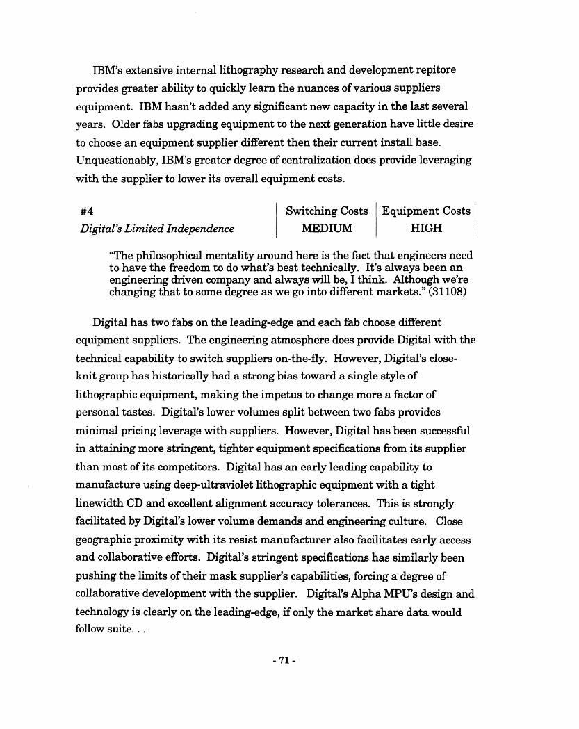
IBM's extensive internal lithography research and development repitoreprovides greater ability to quickly learn the nuances of various suppliers
equipment. IBM hasn't added any significant new capacity in the last several
years. Older fabs upgrading equipment to the next generation have little desire
to choose an equipment supplier different then their current install base.Unquestionably, IBM's greater degree of centralization does provide leveraging
with the supplier to lower its overall equipment costs.
#4 Switching Costs Equipment Costs
Digital's Limited Independence MEDIUM HIGH
"The philosophical mentality around here is the fact that engineers needto have the freedom to do what's best technically. It's always been anengineering driven company and always will be, I think. Although we'rechanging that to some degree as we go into different markets." (31108)
Digital has two fabs on the leading-edge and each fab choose different
equipment suppliers. The engineering atmosphere does provide Digital with the
technical capability to switch suppliers on-the-fly. However, Digital's close-
knit group has historically had a strong bias toward a single style of
lithographic equipment, making the impetus to change more a factor of
personal tastes. Digital's lower volumes split between two fabs provides
minimal pricing leverage with suppliers. However, Digital has been successful
in attaining more stringent, tighter equipment specifications from its supplier
than most of its competitors. Digital has an early leading capability tomanufacture using deep-ultraviolet lithographic equipment with a tight
linewidth CD and excellent alignment accuracy tolerances. This is strongly
facilitated by Digital's lower volume demands and engineering culture. Close
geographic proximity with its resist manufacturer also facilitates early accessand collaborative efforts. Digital's stringent specifications has similarly been
pushing the limits of their mask supplier's capabilities, forcing a degree of
collaborative development with the supplier. Digital's Alpha MPU's design and
technology is clearly on the leading-edge, if only the market share data wouldfollow suite...
- 71 -
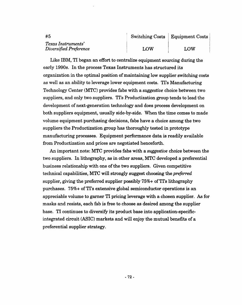
#5 Switching Costs Equipment Costs
Texas Instruments'Diversified Preference LOW LOW
Like IBM, TI began an effort to centralize equipment sourcing during the
early 1990s. In the process Texas Instruments has structured its
organization in the optimal position of maintaining low supplier switching costs
as well as an ability to leverage lower equipment costs. TI's Manufacturing
Technology Center (MTC) provides fabs with a suggestive choice between two
suppliers, and only two suppliers. TI's Productization group tends to lead the
development of next-generation technology and does process development on
both suppliers equipment, usually side-by-side. When the time comes to made
volume equipment purchasing decisions, fabs have a choice among the two
suppliers the Productization group has thoroughly tested in prototype
manufacturing processes. Equipment performance data is readily availablefrom Productization and prices are negotiated henceforth.
An important note: MTC provides fabs with a suggestive choice between the
two suppliers. In lithography, as in other areas, MTC developed a preferential
business relationship with one of the two suppliers. Given competitive
technical capabilities, MTC will strongly suggest choosing the preferred
supplier, giving the preferred supplier possibly 75%+ of TI's lithography
purchases. 75%+ of TI's extensive global semiconductor operations is an
appreciable volume to garner TI pricing leverage with a chosen supplier. As for
masks and resists, each fab is free to choose as desired among the supplier
base. TI continues to diversify its product base into application-specific-
integrated circuit (ASIC) markets and will enjoy the mutual benefits of a
preferential supplier strategy.
- 72 -
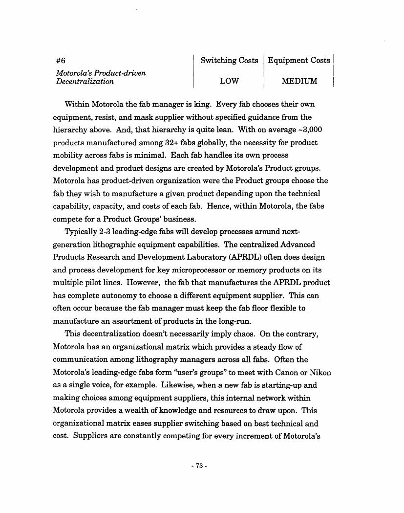
#6 Switching Costs Equipment Costs
Motorola's Product-drivenDecentralization LOW MEDIUM
Within Motorola the fab manager is king. Every fab chooses their own
equipment, resist, and mask supplier without specified guidance from thehierarchy above. And, that hierarchy is quite lean. With on average -3,000
products manufactured among 32+ fabs globally, the necessity for product
mobility across fabs is minimal. Each fab handles its own process
development and product designs are created by Motorola's Product groups.
Motorola has product-driven organization were the Product groups choose the
fab they wish to manufacture a given product depending upon the technical
capability, capacity, and costs of each fab. Hence, within Motorola, the fabs
compete for a Product Groups' business.
Typically 2-3 leading-edge fabs will develop processes around next-
generation lithographic equipment capabilities. The centralized Advanced
Products Research and Development Laboratory (APRDL) often does design
and process development for key microprocessor or memory products on its
multiple pilot lines. However, the fab that manufactures the APRDL product
has complete autonomy to choose a different equipment supplier. This can
often occur because the fab manager must keep the fab floor flexible to
manufacture an assortment of products in the long-run.This decentralization doesn't necessarily imply chaos. On the contrary,
Motorola has an organizational matrix which provides a steady flow ofcommunication among lithography managers across all fabs. Often the
Motorola's leading-edge fabs form "user's groups" to meet with Canon or Nikon
as a single voice, for example. Likewise, when a new fab is starting-up and
making choices among equipment suppliers, this internal network withinMotorola provides a wealth of knowledge and resources to draw upon. This
organizational matrix eases supplier switching based on best technical andcost. Suppliers are constantly competing for every increment of Motorola's
- 73 -
business. This competitive atmosphere applies pressure among suppliers to
lower pricing, yet pricing-by-volume is limited by the size of the fab.
Internal Metrics of the Success of Equipment Sourcing Strategies
"Just the fact that we're making money. We've been pretty successful.It's kind of a given. It's like, I'm a human being and I am living on Earth,that's the way things happen at Motorola, that's the way it's going to be,and no one is going to change it. And it seems to be working." (51012)
The above comment encapsulates the feeling of the semiconductor industry.
Fundamentally, the lithography equipment they have chosen has functionedappropriately, through their given sourcing methods they feel like they're
reducing capital costs, and have successfully reduced time-to-money. (51012)
Few companies have hard metrics for measuring the success of their
equipment sourcing strategy. In addition, the 3-4 year cycle time forintroducing new lithographic generations makes the effort of comparative
study difficult.
3.6. Supplier Relations & Equipment Evaluation:The 7 Steps to Lithography Equipment Sourcing
_uA__z ~ -_
There is a spectrum of customer-supplier relations in the semiconductor
lithography realm along three points: (1) An arms-length relationship were
contact occurs on an as needed basis between customer and supplier, (2) The
supplier is among a core network of preferred suppliers with periodic
communications established, and (3) A supplier as a long-term, strategic
partner with frequent interactions. (42065) One could pick any customer-
supplier pair and place them on this continuum. Most semiconductorcompanies would rather not have it publicly known the degree of closeness
they have with their supplier. Given that manufacturers often compete for theattention and leverage on their suppliers, the details of their relationship
- 74-

becomes an issue of confidentiality. In any case, each supplier managementstrategy brings its own rewards and drawbacks.
There is a strong tendency towards the center of the spectrum amongmanufacturers. Having a preferred supplier is seemingly far more favorable
than the extremes of arms-length or strategic partner. In an arms-lengthrelationship there is little response from the supplier to meet your needs. On
the other extreme, there is a feeling of being locked into one supplier and at
their mercy, i.e. high supplier switching costs. Preferred suppliers provides the
favoritism of economies-of-scale with a given supplier, get their attention for
your specific concerns, and often provides an avenue for feedback of possible
improvements. In essence, a business relationship while maintaining aresidual supplier switching capability as needed. Consider for example onoe
perspective from a very profitable semiconductor manufacturer:
"We operate with all suppliers of key products exactly the same, sharinginformation, working very closely with them. But the choice isn't there.We don't have any long-term strategic partners. We have long-termcompanies, companies we do business with. This thing of strategicparnters, I find it a hateful concept. It says, "You can screw me, butyou're my partner, so I forgive you." It's a business relationship basedupon neutral profitability. That describes our relationship will all oursuppliers, whether its steppers, tracks, ashers, resist suppliers, etc."(42065)
The tool consistently used to designate a preferred supplier is through an
approved equipment supplier list. With the exception of Motorola, everyonehas some form of listing their suppliers of choice. Intel may call it the Plan of
Record or Texas Instruments may call it a supplier alliance, but the concept is
the same: selecting a given suppliers equipment as the production tool of
choice for a technology generation.
Getting on the approved list, or more simply, to be the chosen requires a
lengthy evaluation process. Figure 3.10 is the semiconductor industry's plain,vanilla seven step equipment sourcing process. Manufacturers tend to go
through these seven stages in evaluating, choosing, and installing lithographyequipment.
- 75 -

Vanilla 7 Step Equipment Sourcing
Customer has basic specificationsdesired for next generation
lithography equipment )
Solicits suppliers to see if theycan meet desired specifications,inquire o sup pliers oltermgs.
Customer chooses select numberof suppliers to perform on-site
eauipmen' . evaluation . )
I
Decision process and customercalculation of best supplier
r_ an _- ____ a_ 1 __ -__ _ _ _ a
Negotiate with 1-2 supplier ontechnical details, support, andpricing for a s
D
peciied volume J
Certification of equipment6 specifications are met once
received before payment is made
Installation &Volume Manufacturing
FIGURE 3.10
- 76 -
1
2
(
C
4C
5C
7
r
{ _
w vI� '
,l!
_ .... ... ........ ......... ... . ...
S ' ' Ha'- * * *6 * *' ' --
u u
_ .. -
! !~ ~ ~ ~
)
I
tnr tPilr mamlT1 tatnll1r nleds
_
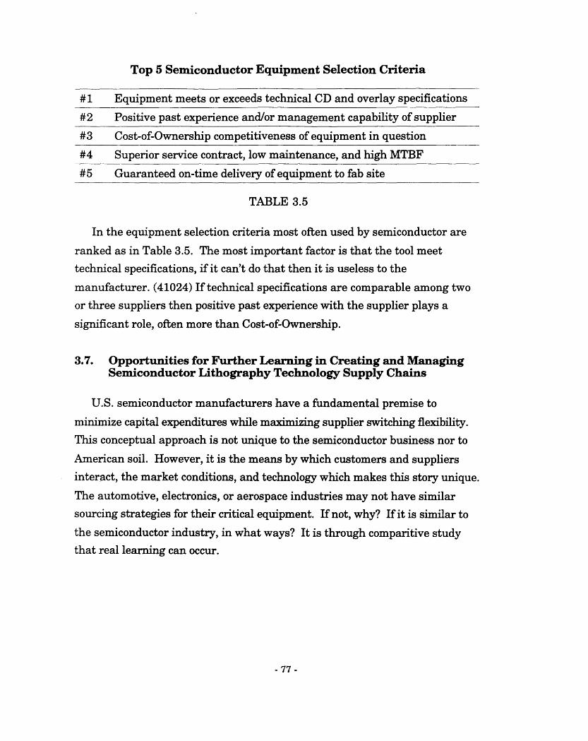
Top 5 Semiconductor Equipment Selection Criteria
#1 Equipment meets or exceeds technical CD and overlay specifications
#2 Positive past experience and/or management capability of supplier
#3 Cost-of-Ownership competitiveness of equipment in question
#4 Superior service contract, low maintenance, and high MTBF
#5 Guaranteed on-time delivery of equipment to fab site
TABLE 3.5
In the equipment selection criteria most often used by semiconductor are
ranked as in Table 3.5. The most important factor is that the tool meettechnical specifications, if it can't do that then it is useless to the
manufacturer. (41024) If technical specifications are comparable among two
or three suppliers then positive past experience with the supplier plays a
significant role, often more than Cost-of-Ownership.
3.7. Opportunities for Further Learning in Creating and ManagingSemiconductor Lithography Technology Supply Chains
U.S. semiconductor manufacturers have a fundamental premise to
minimize capital expenditures while maximizing supplier switching flexibility.
This conceptual approach is not unique to the semiconductor business nor to
American soil. However, it is the means by which customers and suppliersinteract, the market conditions, and technology which makes this story unique.
The automotive, electronics, or aerospace industries may not have similar
sourcing strategies for their critical equipment. If not, why? If it is similar to
the semiconductor industry, in what ways? It is through comparitive studythat real learning can occur.
- 77 -

Likewise, the U.S. semiconductor industry does not exist in isolation.
Learning how Japanese, Korean, and European semiconductor companies cope
with the industry cyclicality and managing their lithography supply chains is ofequal interest. Does the differences of cultural or geographic proximity provide
NEC a completely different sourcing strategy than IBM. Are they equally
effective? Are the objectives truly the same?
- 78 -

Chapter 4
APPENDIX
- 79 -

TSC Symposium Breakfast Presentation
Learning fromLithography Equipment Technology
Supply Chain Managementin the Semiconductor Industry
Corporate Equipment Sourcing Strategiesto Maximize Supplier Switching Flexibility
while Minimizing Capital Expenditures
Thursday, May 11 Charles PieezulewekiTwenty Chimneys Room Masts Thei SeminarStratton Student Center Preentation 7:45 a.m.MIT Bldg. W20-306 Breakfat 7:30 .m.
What is Lithography Equipment?
Imagine a tool that...* Limits the performance measures your
customers use in choosing your products
· If improved, single-handedly lowers yourmanufacturing cost per unit
· Most expensive set of tools in your factory
a Limited number of suppliers in the worldcapable of providing this tool
Criticality of Lithography to theSemiconductor Industry
*Providing consumer demand for faster,cheaper, and lower power electronicsis enabled by lithography technology
* 10% Reduction in chip size =10% reduction in cost per chip
*33% of Capital Equipment Costs fornew $1 billion manufacturing fabs
*Only 4 Leading-Edge Suppliers WW:Nikon, Canon, ASML, & SVGL
U
- 80 -
i. .. i

Lithography Knowledge in theHands of Equipment Suppliers
Make Buy
* Management SupplyChain
Internal ManagementDevelopment
Issues:Cost Effectiveness
Sources of InnovationLocus of Technology Know-How
Manufacturer's CHOICE: Focus on Supply Chain Management
Long Time Constant for LearningSupply Chain Management
Be Ti 3..0 PPOo D I 10
_ Iun.. _ I-* I ..-Sin.rInd s r * . D_, :ru C .b
Lithography TechnologyInterdependency & Dependency
Lack of In-House CapabilityAmount of Work has forced interdependency:Dons In-hou Done \ *houn Ieuning 6s. Conortium
+-/+ ,> * Industry Steps In-concert·SIA, SEMATECH, SRC
Internal Amount ofCapab' ity I~.rn Dependency on Supplier has
diminished In-house Work:- · Industry-wide outourcing of
lithography upport technologies* Purchase Off-the-Shelf solutions
Free Acce to Leading-EdgeLithography Technology
- 81 -
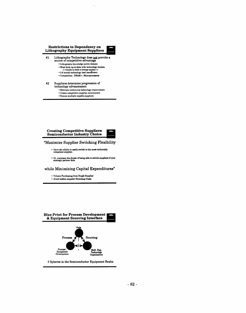
Restrictions to Dependency onLithography Equipment Suppliers
#1 Lithography Technology does mnt provide asource of competitive advantage
* Lithography knowledge public domain* Must keep up-to-date with technology leaders
>> Cmp.q o abili to e pplk <
* 3-6 month technology lead inufficient* Competition: DRAM v. Microprocessors
#2 Suppliers determine progression oftechnology advancement
· Motivate continuous technology improvement· Create competitive supplier environment· Ensure multiple capable suppliers
Creating Competitive Suppliers:Semiconductor Industry Choice
"Maximize Supplier Switching Flexibility
· Have the ability to easily switch to the most technicallycompetent supplier.
· Or, maintain the threat of being able to switch suppliers if yourstrategic partner fails.
while Minimizing Capital Expenditures"
* Volume Purchasing from Single Supplier· Avoid hidden supplier Switching Costs
Blue-Print for Process Development& Equipment Sourcing Interface
Process
EquipmentDevelopment
cing
Mfc. Eao.Technology
Organization
3 Spheres in the Semiconductor Equipment Realm
- 82 -

Centralized - DecentralizedInternal Equipment Sourcing U
F.b Fb
Fa. Pb - .. h
Centralized Decentralized"Time to Money"
Measurement of Supplier Closeness
Semiconductor Industry Tendency for Center'Preferred Supplier'
Examples ?
Supplier Preference viaApproved Equipment List a
PROS CONS* Reduces redundant * Promotes Single
activities at multiple Supplier Allegiancefabs
* Volume discount * 2-3 Generations withpurchasing from same supplier weakenssupplier switching ability
* Reduces equipmentevaluation costs Motorola: Optimal Supplier
* Product manufacturing SwitMlig Condition VolumePricing via Multiple Large Faab,mobility across all labs Diverified Product Bas
- 83 -
I�m�all�RI IUILo·m�Ulp� �ll�mlYRlwl
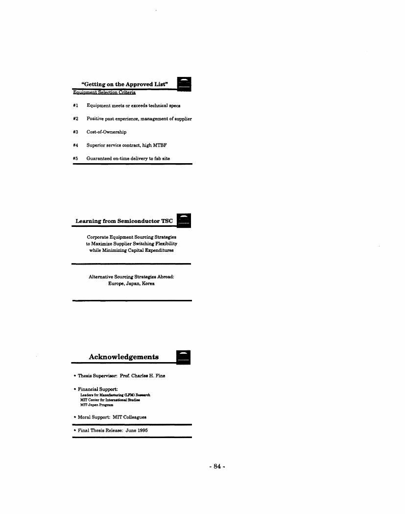
"Getting on the Approved List"Eauipment Selection Criteria
#1 Equipment meets or exceeds technical sp,
#2 Positive past experience, management of
#3 Cost-of-Ownership
#4 Superior service contract, high MTBF
#5 Guaranteed on-time delivery to fab site
ecs
supplier
Learning from Semiconductor TSC
Corporate Equipment Sourcing Strategiesto Maximize Supplier Switching Flexibility
while Minimizing Capital Expenditures
Alternative Sourcing Strategies Abroad:Europe, Japan, Korea
Acknowledgements U* Thesis Supervisor Prof. Charles H. Fine
* Financial Support:Leader for Manfcturing (M) RearchMIT Center for Inteational StudierMIT-Japan Program
* Moral Support: MIT Colleagues
* Final Thesis Release: June 1995
- 84 -
I
4.2. Sample Questions from Corporate Survey
32152 How is the semiconductor equipment sourcing group organized?What people are involved in the sourcing process? Is the sourcinggroup organized to negotiate both technical and financial terms of thecontract?
32150 Does AMD have an approved equipment or vendors list?
YES NO
If yes, how does the equipment and/or vendor get on the approvedlist? If yes, What function does the "approved equipment" list servefor AMD?
31108 Is the lithography equipment purchasing decisions for AMD's new fablines centralized at one location or does each fab choose its ownequipment independently?
42057 If your current lithography equipment supplier, Canon for example,somehow loses their technological and/or cost competitive edge overcompetition, what is the likely steps AMD would take?
Switch suppliers at next opportunityGive supplier a deadline by which to resolve problem themselvesOffer technical assistance to supplier in any way reasonably possibleOther, please specify:
42055 Does AMD form formal relationships with strategic equipmentsuppliers of lithography technology?
YES NO
If NO, is this a conscious decision or a particular reason not to do so?If YES, what was the motivations for forming an alliance?
11028 If in your current 0.5 pm fab you have Nikon steppers in use, whatwould be the costs incurred if you switched to Canon or SVGLsteppers for the 0.35 pm generation fab?
- 85 -

D
- l
- 86-


![2 LASER INTERFERENCE LITHOGRAPHY - uni-halle.de · 2 LASER INTERFERENCE LITHOGRAPHY (LIL) 9 2 LASER INTERFERENCE LITHOGRAPHY (LIL) Laser interference lithography [3~22] (LIL) is a](https://static.fdocuments.in/doc/165x107/5eae180eecc7e273a41a4e88/2-laser-interference-lithography-uni-hallede-2-laser-interference-lithography.jpg)